Article

Optoelectronic and Electrochemical Properties of Vanadium Pentoxide Nanowires Synthesized by Vapor-Solid Process

Institute of Manufacturing Technology and Department of Mechanical Engineering, National Taipei University of Technology (TAIPEI TECH), Taipei 10608, Taiwan
*
Author to whom correspondence should be addressed.
Nanomaterials 2016, 6(8), 140; https://doi.org/10.3390/nano6080140
Submission received: 31 May 2016 / Revised: 11 July 2016 / Accepted: 19 July 2016 / Published: 29 July 2016

Abstract

:
Substantial synthetic vanadium pentoxide (V2O5) nanowires were successfully produced by a vapor-solid (VS) method of thermal evaporation without using precursors as nucleation sites for single crystalline V2O5 nanowires with a (110) growth plane. The micromorphology and microstructure of V2O5 nanowires were analyzed by scanning electron microscope (SEM), energy-dispersive X-ray spectroscope (EDS), transmission electron microscope (TEM) and X-ray diffraction (XRD). The spiral growth mechanism of V2O5 nanowires in the VS process is proved by a TEM image. The photo-luminescence (PL) spectrum of V2O5 nanowires shows intrinsic (410 nm and 560 nm) and defect-related (710 nm) emissions, which are ascribable to the bound of inter-band transitions (V 3d conduction band to O 2p valence band). The electrical resistivity could be evaluated as 64.62 Ω·cm via four-point probe method. The potential differences between oxidation peak and reduction peak are 0.861 V and 0.470 V for the first and 10th cycle, respectively.

1. Introduction

Vanadium pentoxide, V2O5, has been fully exploited in electrochemical energy storage, catalysis and gasochromic coloration [1,2,3,4,5,6,7]. In general, V2O5 nanostructures are highly regarded by researchers due to their redox-activity and layered structures, which provide the inserts for electrochemical intercalation/deintercalation of lithium ions [8,9]. Some published literatures disclose the practical applications of V2O5 nanostructure, including electrochemical super-capacitors and energy storage gadgets [10,11,12]. Also, compared to several thin film materials, low-dimensional vanadium oxide nanostructures are functional as well as attractive as gas sensors of hydrogen [13,14]. In addition, coating platinum (Pt) as a catalyst on V2O5 nanostructures makes reactions with hydrogen easy, meaning that they could behave much more sensitively toward the leakage of hydrogen than uncoated V2O5 nanostructures. It should be noted that many technical methods, namely hydrothermal synthesis [15,16], sol-gel process [17,18] and evaporation-condensation growth [19,20], have been rapidly expanded in the syntheses and formation of one-dimensional V2O5 nanostructured materials; however, very little of the previous research about fabricating V2O5 nanowires concerns the VS method. The VS method belongs to a bottom-up process in fabricating nanostructured materials, which uses a gas atom or a gas molecular as the basis unit from which chemical vapor deposition (CVD) is developed. Generally, the gas atom or gas molecular of materials is directly deposited on the substrate, which is quite different from vapor-liquid-solid (VLS) and solid-liquid-solid (SLS) approaches. Both VLS and SLS approaches need catalysts as the precursors, which act as an intermedium in the adsorption of growth species. In other words, the catalysts in the VLS and SLS methods are the nucleation sites leading to the growth of nanostructured materials. In terms of the VS method, Zhao et al. [21] synthesized large-scale GaN nanorods via this method. The appearance of the GaN nanorods is cone-tip and the GaN nanorods might be grown along the screw dislocations, so the GaN nanorods belong to a spiral growth mechanism.
Yang et al. [22] adopted VS growth to employ magnesium oxide (MgO) nanowires on MgO substrates, and two noteworthy features of nucleation sites have thus been exhibited:
  • The MgO substrates are etched in 0.5 M NiCl2 solutions for 1 to 30 min to create nanoscale pits/projections, then the depositions of MgO nanowires have been grown on the nanoscale pits/projections of MgO (100) substrates by VS method. In other words, the nanoscale pits/projections are the nucleation sites of this VS method.
  • The MgO nanowires are directly grown on the MgO substrates without etching process. At the beginning of this reaction, the MgO nanoscale particles are deposited on the surface of MgO substrates, which include plenty of defects, i.e., steps, kinks and so on. These defects are the nucleation and the oriented growth of MgO nanowires.
In this task, a very simple and efficient fabrication, thermal evaporation, was presented to synthesize V2O5 nanowires via VS method. The samples were characterized by scanning electron microscopy (SEM), energy-dispersive X-ray spectrometer (EDS), X-ray diffraction (XRD) and transmission electron microscopy (TEM). Regarding the optoelectronic property, the luminescence and electronic property of the synthesized V2O5 nanowires were investigated by photo-luminescence (PL) spectrum and the four-point probe method, respectively. Furthermore, the performance of electrochemical examination was recorded by cyclic voltammetry (CV).

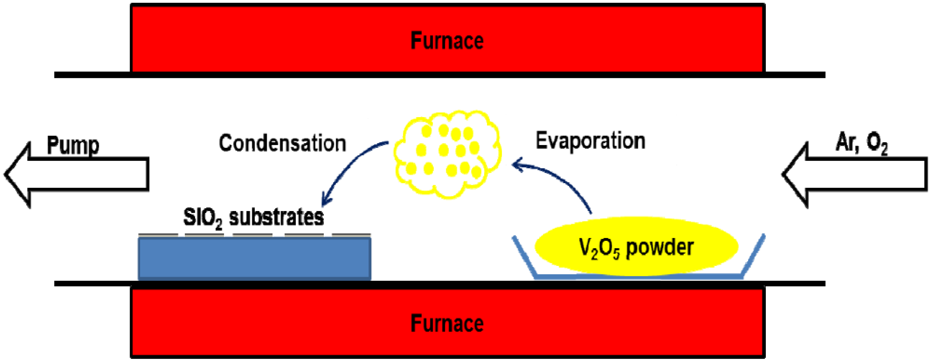
2. Experimental Method

V2O5 nanowires were fabricated on silicon substrates, a commercial item with a growth plane of (100), by thermal evaporation. Good quality 0.5 g V2O5 powders (Alfa, purity 99.5%, 325 mesh, Heysham, Lancashire, UK) and several silicon substrates were situated in an aluminum oxide (Al2O3) boat, and then the Al2O3 boat was placed in the heating area of a quartz tube, as illustrated in Figure 1. These substrates employed in this experiment are commercial silicon wafers of (001). In advance, The Si substrates were prepared without chemical etchings or physical damage, but were cleaned ultrasonically in acetone. During the growth of V2O5 nanowires, the pressure inside the quartz tube was maintained at 0.5 Torr by a rotary pump. The working parameters of this process were as follows: (1) Increasing the working temperature to 800 °C with 26 °C/min was at a continual flow rate of 30 sccm Ar gas; (2) Maintaining the temperature at 800 °C for 1 h was at a constant flow rate of combined gas of 30 sccm Ar and 30 sccm O2; (3) Cooling to the room temperature was under a constant flow rate of 30 sccm of Ar gas.
The morphology, crystal structure and chemical composition of the V2O5 nanowires were analyzed by a field emission scanning electron microscope (FESEM, Zeiss, SIGMA Essential, Jena, Germany), a high-resolution transmission electron microscope (HRTEM, JEOL, JEM-2010, Tokyo, Japan), a MAC glancing incident X-ray spectrometer with an incident angle of 0.5° (PANalytical, Almelo, The Netherlands), and energy-dispersive X-ray spectroscopy (EDS, Bruker, Hanau, Germany), respectively. Regarding the optical property of V2O5 nanowires, the measurement via PL (RENISHAW inVia, Wotton-under-Edge, UK) at room temperature under an irradiation (λ = 325 nm, 20 W/m2) of wavelength from 300 to 800 nm was undertaken. As for the electronic property of single V2O5 nanowire, the sample with regard to the electronic measurement was prepared by dual-beam focused ion beam system (FIB, FEI Helios Nanolab 600i System, Hillsboro, OR, USA), then the I-V curve was characterized between −3 V and 3 V by Keithley 4200 (Solon, OH, USA).
With respect to inquiring into the electrochemical properties of V2O5 nanowires, the cyclic voltammetric curve was plotted by an Electrochemical Workstation (CHI 627E, Austin, TX, USA) to investigate the potential of oxidation peak and reduction peak. The test cell includes three kinds of electrodes and one electrolyte in a beaker. A saturated calomel electrode (SCE) and a platinum foil were adopted as the reference electrode and counter electrode, separately. The working electrode was fabricated by mixing 80 wt. % V2O5 nanowires, 10 wt. % polyvinylidene difluoride (PVdF) and 10 wt. % carbon black in N-methyl pyrrolidinone (NMP) solvent to become a slurry. The slurry was spread onto an Al2O3 foil and evenly distributed on the Al2O3 foil, then the sample was placed in the oven to transform slurry into a solid. A volume of 2 M KCl aqueous solution was prepared as the electrolyte in the beaker-style three-electrode test cell. The cyclic voltammetry (CV) was conducted in a voltage range between −2 and 2 V at 50 m·VS−1 scan rate at room temperature.

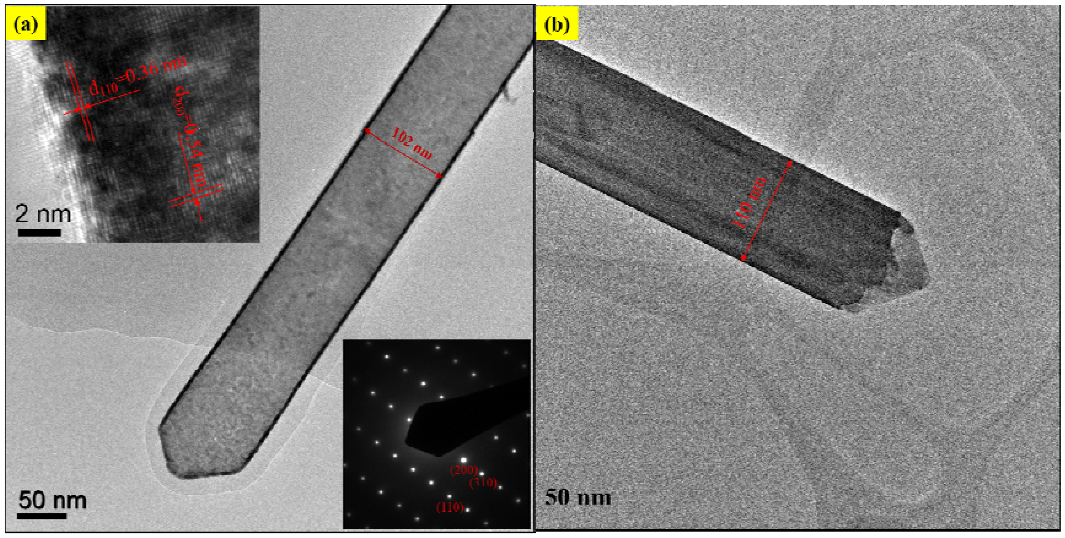
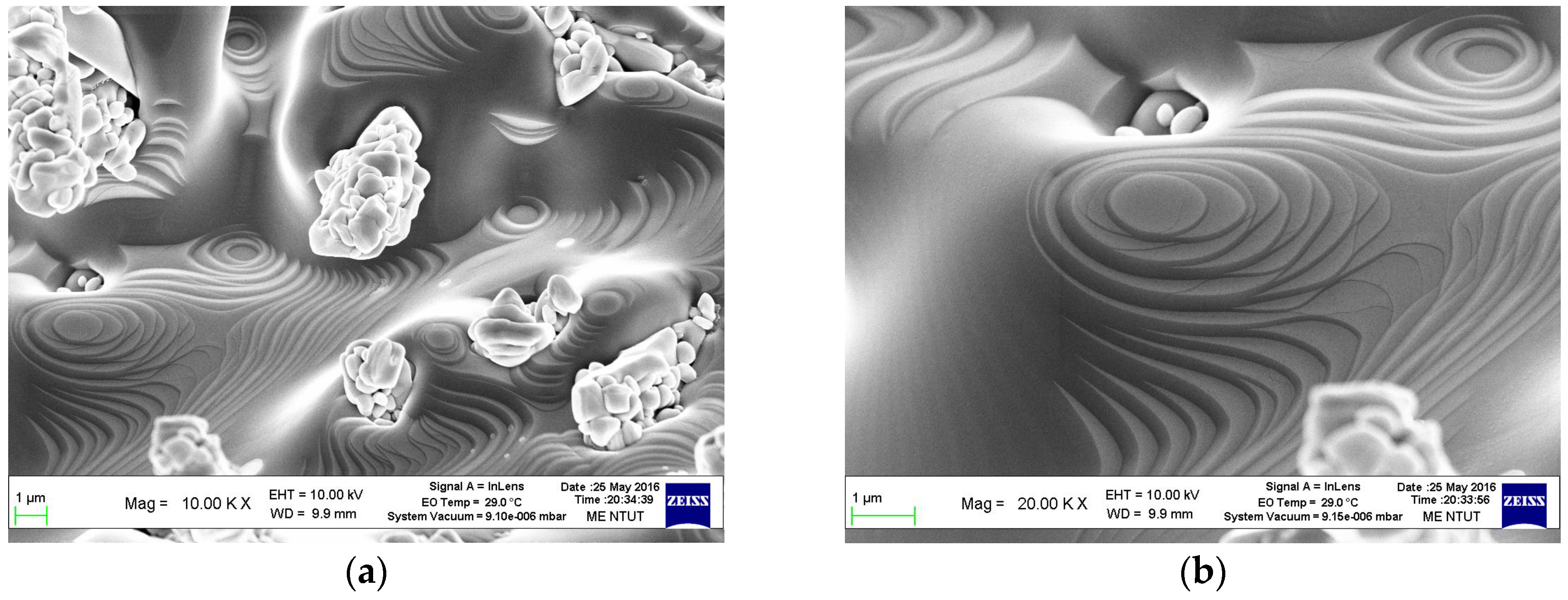
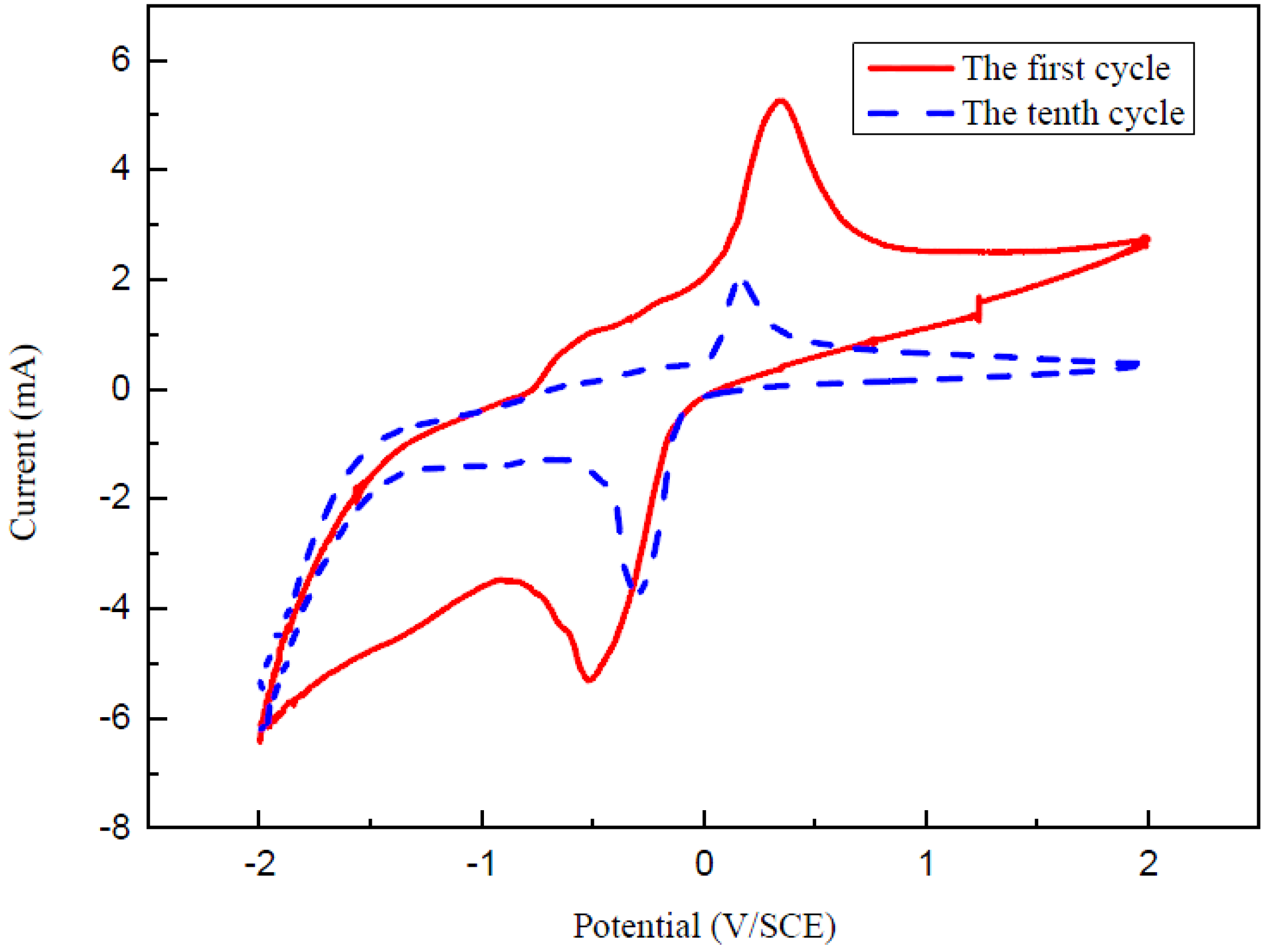
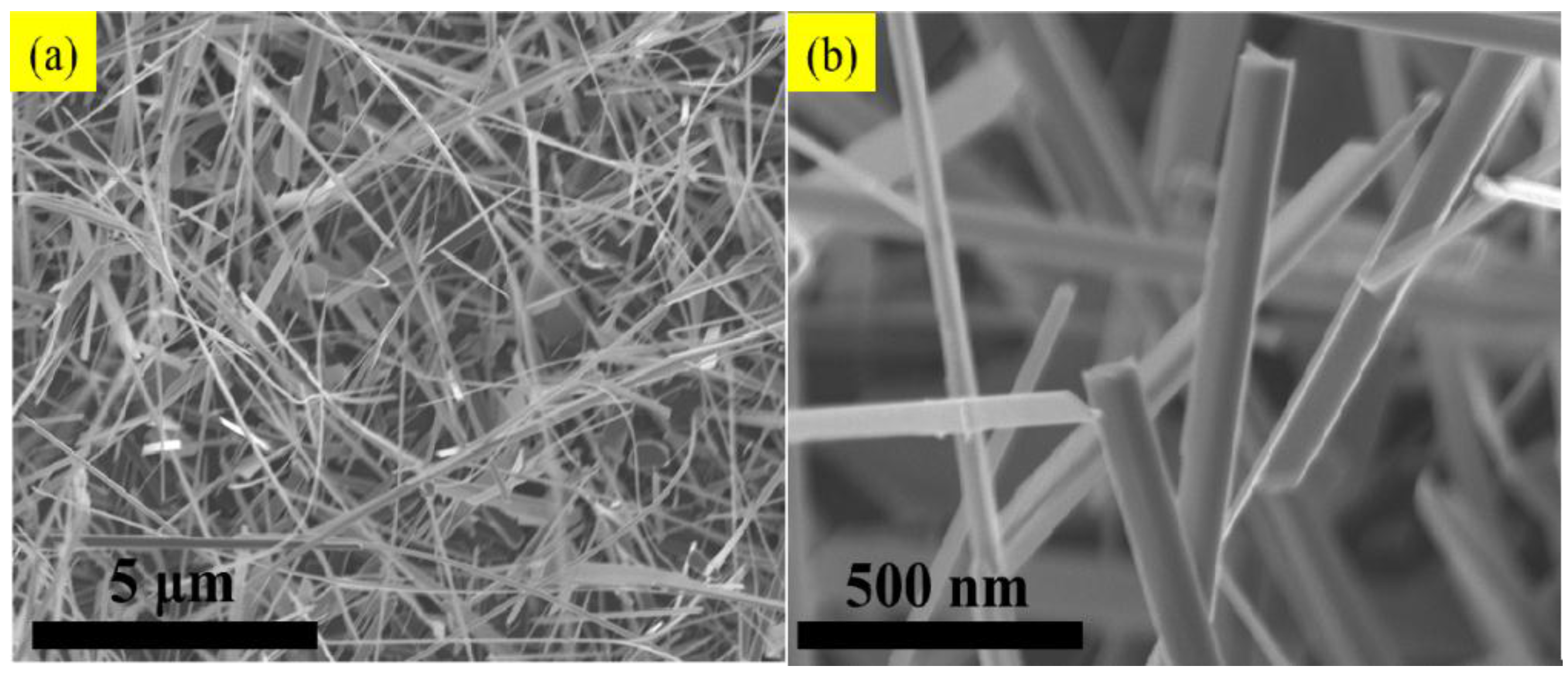
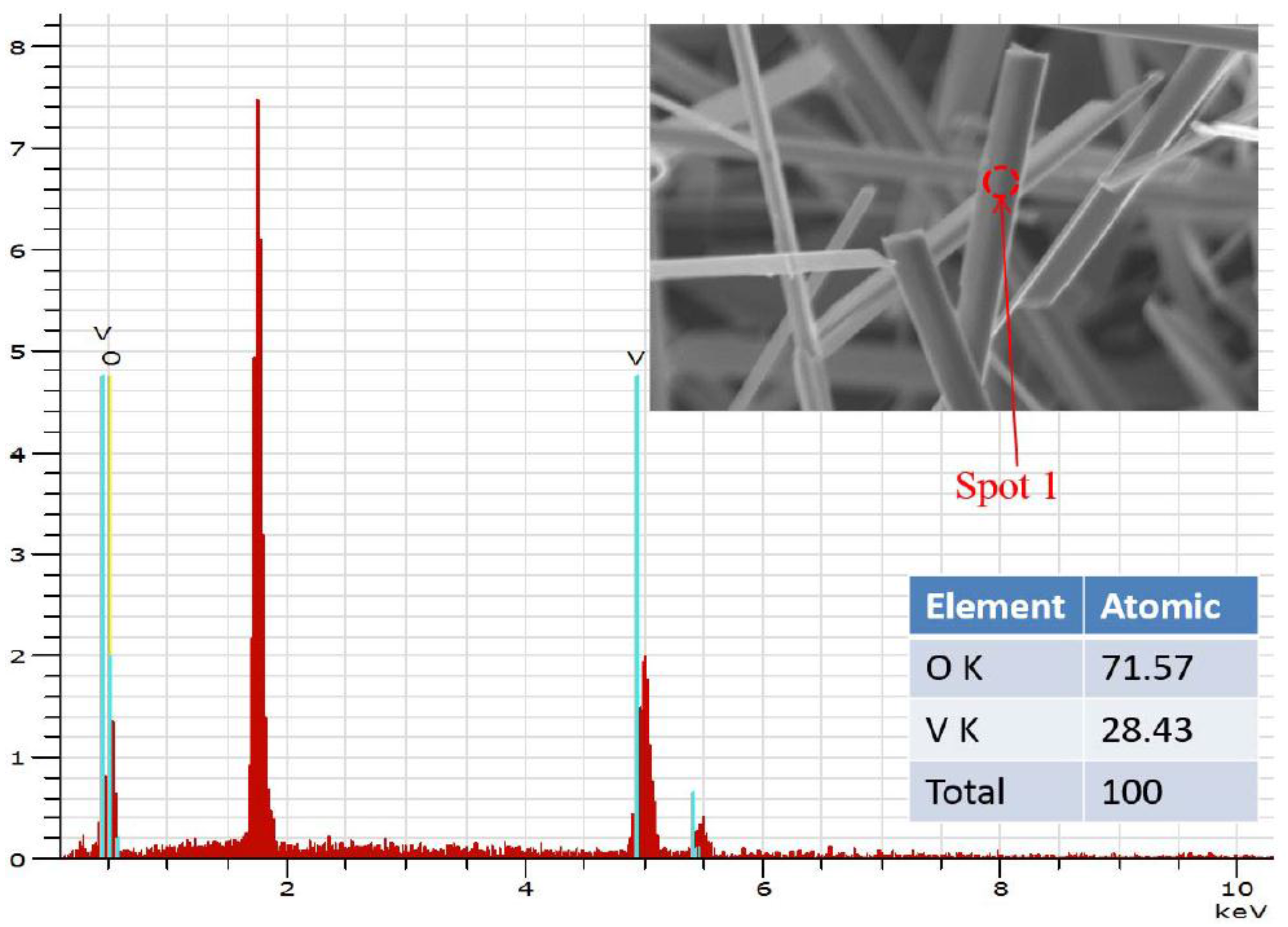
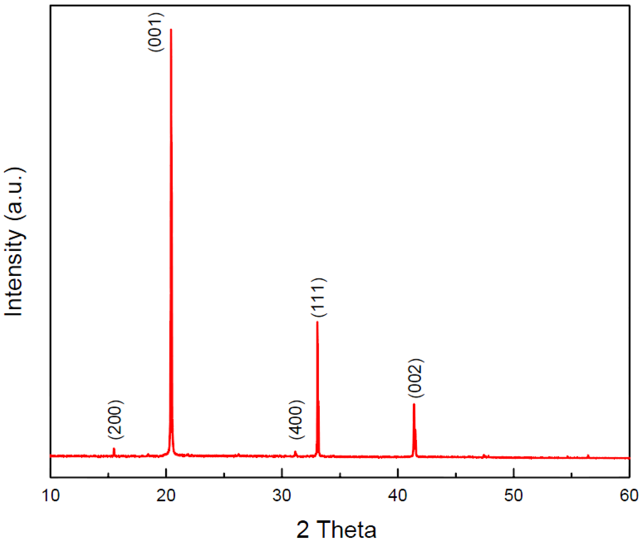
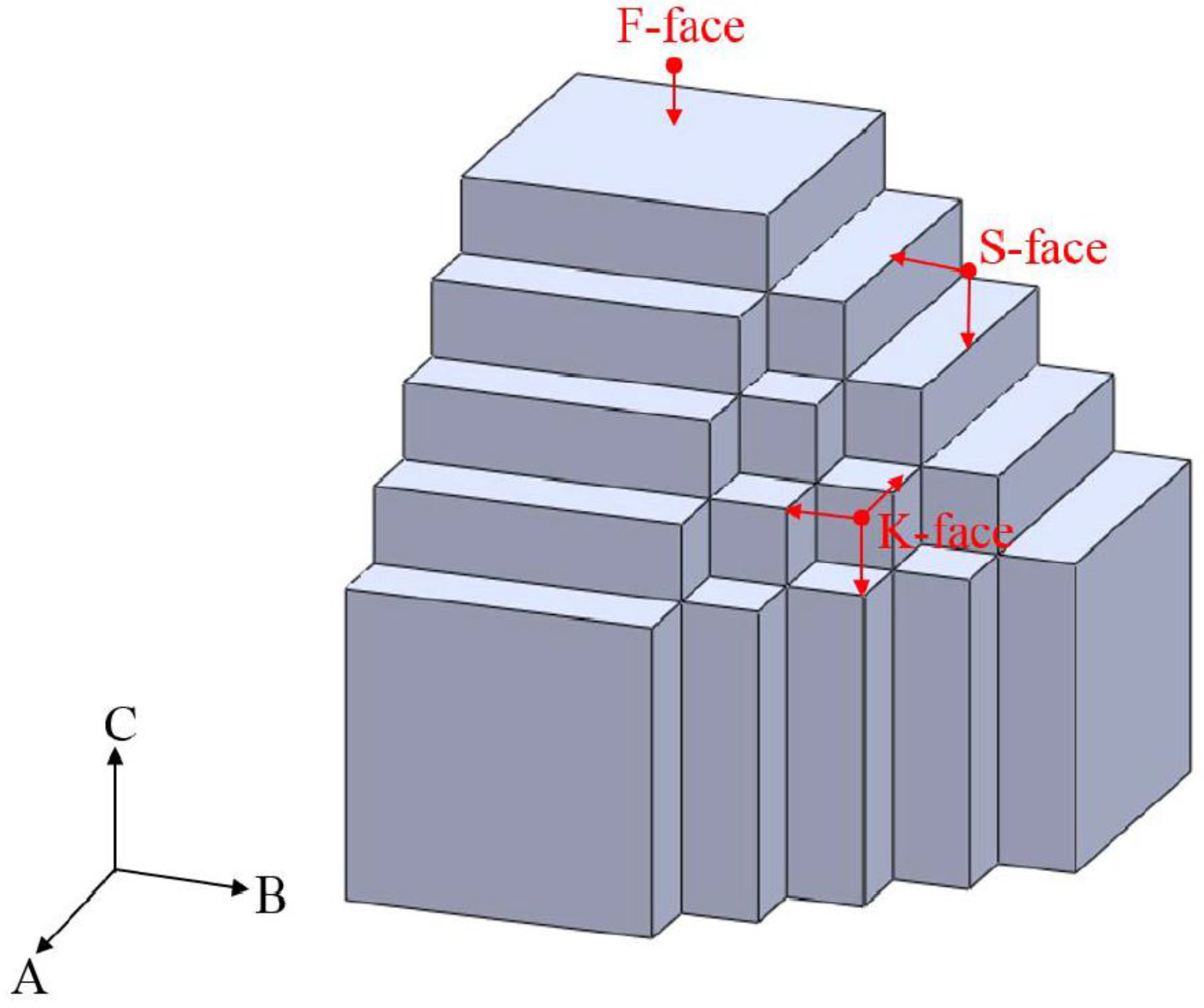
3. Results and Discussion

Figure 2 shows the SEM image of abundant V2O5 nanowires with diameter about 100 nm and length more than 10 μm, which have been prepared by the VS process. The micromorphology and microstructure of one single V2O5 nanowire were further investigated by observation of TEM. Figure 3, the EDS of spot 1 on the surface indicates the co-existence of V and O, and the percentages of V and O of an atom are 28.43 and 71.57, which is approaching to the ratio of V2O5. Herein, the above examinations totally testify to fabricate V2O5 nanowires effectively via this VS process. The XRD pattern of V2O5 nanowires is illustrated in Figure 4 exhibiting peaks of 2θ angles at 15.4°, 20.3°, 33.3°, and 41.3° corresponding to the reflection of (200), (001), (111) and (002) crystalline planes in the orthorhombic structure of V2O5, which makes a comparison of JCPDS: 77–2418, signifying that its structure belongs to Pmmn and lattice parameters a, b and c are 11.51 Å, 3.564 Å and 4.368 Å, respectively. By calculating with Scherrer equation: d = 0.9 λ/B cosθ (where d is grain diameter, λ is wavelength of the X-ray = 0.1541 nm (Cu-Kα), B is full width at half max of specific peak), the grain size is about 98.9 nm of (001). To observe the surfaces of V2O5 nanowires exactly, the low-magnification TEM image of a sample was taken in Figure 5a,b, and we demonstrated that the diameters of V2O5 nanowire are 102 and 110 nm, respectively. The upper left inset is HRTEM image of a V2O5 nanowire and the lower right inset is the selected-area-electron-diffraction (SAED) pattern of a V2O5 nanowire. After confirmation, one-dimensional V2O5 nanowires grow along the (110) plane with the interplanar spacing of 0.36 nm, which corresponds to the (110) plane of V2O5. Judging from the tip of a single V2O5 nanowire in Figure 5, the cone-tip is observed to be a proof of spiral growth mechanism [21,22,23]. As mentioned in the introduction and experimental method sections, the substrates were prepared without any preparations, for example, sputtering precursors, chemical and physical etchings processes. Therefore, the formation of V2O5 nanowires through the VS process is due to anisotropic growth and its growth mechanism is the screw dislocation in the crystal plane of (110).
Herein, the crystal growth via using VS process could be explained by Burton, Cabrera and Frank (BCF) theory [24]. In 1951, three outstanding scientists, Burton, Cabrera and Frank, promulgated a well-known paper “The growth of crystals and the equilibrium structure of their surface” [25], and a famous theory, BCF theory, was established to account for the growth of a crystal face in the presence of screw dislocations. In view of BCF theory [24,25], it should be pointed out that the existence of screw dislocations does not only ensure an advanced source of growth surface, but also achieves better growth rate. Various facets have a considerably different capability to accommodate dislocations, so the prominent role of dislocations on a certain facet can cause anisotropic growth for the formation of nanowires or nanorods. On the other hand, the periodic bond chain (PBC) theory provides a unique perspective in understanding the various growth rates and activities depending on different facets [26,27]. On the basis of PBC theory [26,27], the crystal surfaces are separated into three main groups: F (flat), S (stepped) and K (kinked) planes. In a simple cubic crystal (SCC), a VS process can be simply characterized as following the procedure illustrated in Figure 6. {100} faces belong to flat surfaces, which denotes F-face and they each have one PBC to penetrate one such plane. {110} faces are stepped surfaces, shortened to S-face, with two PBCs. {111} faces are kinked surfaces, abbreviated K-face, with three PBCs. For {110} surfaces, every single surface site is a step or ledge site; hence, any impinging atom would be incorporated wherever it absorbs. In terms of the S-face growth process, it always involves limited adsorption because the accommodation coefficient on {110} is unity, so all impinging atoms are obtained and incorporated into the growth surface. Therefore, in this study, the growth of V2O5 nanowires can be attributed to screw-dislocation-induced anisotropic growth, which is proven by both the TEM images in Figure 5a,b, and the above PBC theory.
Figure 7 shows the SEM images of the sample synthesized at the commencement of V growth species into V2O5 crystal nanostructures, which presents a step-line self-intersecting appearance, thus nucleating an island. Figure 7a,b is very similar to Figure 6, when the growth mechanism is the screw dislocation on the S-face in a SCC. Herein, this result provides clear proof to verify that the crystal growth of V2O5 nanowires is in accordance with the PBC theory. This theory denotes that the V2O5 nanowires grow along the {110} direction in VS process, so screw dislocations are required for the continued growth on a {110} surface that belongs to an S-face in PBC theory.
In order to evaluate the optical property, as depicted in Figure 8, the PL spectrum of V2O5 nanowires is recorded from 300 to 800 nm in the scale of wavelength at room temperature. Three luminescence peaks display the correspondence between the locations at 400, 560 and 710 nm and the photon energies approximated to 3.00, 2.21 and 1.75 eV, respectively. From the previous studies [19,28], the PL emission peaks located at 400 and 560 nm belong to intrinsic transition. Owing to the recombination of electron-hole pair from the bottom of the V 3d conduction band to the top of the O 2p valance band, the intensity of the PL spectrum is centered at 400 nm. The recombination of electron-hole pair from the V 3d split-off conduction band to the top of O 2p valence band causes the PL spectrum to peak at 560 nm. The light emission excited at 710 nm of PL spectrum belongs to extrinsic transition, which is derived from the recombination from the lowest defect donor band to the O 2p valence band. Generally, the defects are oxygen vacancies in V2O5 nanowires. According to the published papers [29,30], orthorhombic crystalline structure of V2O5 is composed of layers of VO5 square pyramids and these VO5 square pyramids regularly link at edges or corners. Additionally, the layers of V-O atoms connect the layers of O atoms in alternate layers along the c-axis. Because the bonding force is an electrostatic force in each layer, formations of oxygen vacancies are done spontaneously in the O layer between the nearest V-O layers in the (001) plane.
Figure 9 demonstrates the measured current-voltage (I-V) curve of a single V2O5 nanowire, which has been measured by the four-point method. Under both the positive and negative bias of 3 V, the I-V characteristic curve shows an almost linear result and indicates a good Ohmic contact between the nanowire and four platinum electrodes. Moreover, the electrical resistivity ( ρ ) could be expressed as
ρ = R × A / L
where R is the resistance of a nanowire; A is the cross section area of a nanowire; L is the length of a nanowire.
From the I-V characteristic curve, the resistance (R) equals 142 × 103 kΩ. According to SEM and TEM images, L and A are equal to 2.3 μm and 102 nm2, respectively. The electrical resistivity could be calculated as 64.62 Ω·cm from Equation (1).
For investigating the electrochemical property of V2O5 nanowires, the CV technique was used to measure the voltages of oxidation peak and reduction peak [31,32]. The typical cyclic voltammetric curve of V2O5 nanowires in 2 M KCl solution at the scan rate of 50 m·Vs−1 at room temperature is plotted in Figure 10. The CV was performed at a potential between −2 V and 2 V. The red CV curve recorded at the first cycle reveals that the reduction peak is located at −0.521 V and the oxidation peak is at 0.340 V, so the potential difference between these two peaks is 0.861 V. The blue dash curve recorded during the 10th cycle shows that the reduction peak is located at −0.308 V and the oxidation peak is at 0.162 V. The potential differences of the red and blue curves are 0.861 V and 0.470 V, respectively. According to these two CV curves, although the CV curve recorded during the 10th cycle becomes small compared with the red curve, the electrochemical performance and reversibility after 10 cycles still remain a good achievement, indicating that using V2O5 nanowires as a cathode is efficient in discharge-charge processes.

4. Conclusions

In summary, after confirmation with SEM, EDS, XRD and HRTEM analyses, the V2O5 nanowires were successfully synthesized on commercial Si substrates via the VS process without using any precursor. The mechanism of V2O5 nanowires grown by the VS process can be described as screw dislocation in the crystal plane of (110). In terms of optical and electronic properties, both examinations of photo-luminescence (PL) spectrum and current-voltage (I-V) curve were carried out. The PL excitation spectrum of V2O5 nanowires exhibits peaks at 400, 560 and 710 nm, which are caused by the various inter-band transitions from V 3d conduction band to O 2p valence band. The electrical resistivity could be assessed at 64.62 Ω·cm via I-V curve. As a result of the above analyses, the V2O5 nanowires exhibited many potential and valuable applications for optoelectronic devices. Moreover, from the CV curves recorded during the 10th cycle, the electrochemical property and durability reveal a good performance, which means that V2O5 nanowires are a promising candidate as the cathodic material in a lithium-ion secondary battery.

Acknowledgments

The authors acknowledge financial support of the main research projects of the Ministry of Science and Technology (MOST) under Grant Nos. 104-2221-E-027-006 and 104-2731-M-027-001.

Author Contributions

Ko-Ying Pan, a postdoctoral fellow, and Da-Hua Wei, an associate professor, at the Institute of Manufacturing Technology and Department of Mechanical Engineering, National Taipei University of Technology (TAIPEI TECH), Taiwan R.O.C., both designed the experiments of this task. Ko-Ying Pan handled the synthesis of V2O5 nanowires and materials analysis, then wrote this article. Da-Hua Wei led this research to the right way and gave the suggestions to enhance the performances of this research work. Mostly, Da-Hua Wei co-wrote and confirmed the whole article.

Conflicts of Interest

The authors declare no conflict of interest.

References

  1. Chen, K.C.; Chen, F.R.; Kai, J.J. V2O5 Nanowires as a Functional Material for Electrochromic Device. Sol. Energy Mater. Sol. Cells 2006, 90, 1156–1165. [Google Scholar] [CrossRef]
  2. Carrero, C.A.; Schloegl, R.; Wachs, I.E.; Schomaecker, R. Critical Literature Review of the Kinetics for the Oxidative Dehydrogenation of Propane over Well-Defined Supported Vanadium Oxide Catalysts. CAS Catal. 2014, 4, 3357–3380. [Google Scholar] [CrossRef]
  3. Wachs, I.E. The Generality of Surface Vanadium Oxide Phases in Mixed Oxide Catalysts. Appl. Catal. A Gen. 2011, 391, 36–42. [Google Scholar] [CrossRef]
  4. Lu, Y.R.; Wu, T.Z.; Chen, C.L.; Wei, D.H.; Chen, J.L.; Chou, W.C.; Dong, C.L. Mechanism of Electrochemical Deposition and Coloration of Electrochromic V2O5 Nano Thin Films: An In Situ X-Ray Spectroscopy Study. Nanoscale Res. Lett. 2015, 10. [Google Scholar] [CrossRef] [PubMed]
  5. Ho, Y.K.; Chang, C.C.; Wei, D.H.; Dong, C.L.; Chen, C.L.; Chen, J.L.; Jang, W.L.; Hsu, C.C.; Chan, T.S.; Kumar, K.; et al. Characterization of Gasochromic Vanadium Oxides Films by X-ray Absorption Spectroscopy. Thin Solid Films 2013, 544, 461–465. [Google Scholar] [CrossRef]
  6. Joseph, B.; Iadecola, A.; Maugeri, L.; Bendele, M.; Okubo, M.; Li, H.; Zhou, H.; Mizokawa, T.; Saini, N.L. Distinct Local Structure of Nanoparticles and Nanowires of V2O5 Probed by X-Ray Absorption Spectroscopy. Appl. Phys. Lett. 2013, 103. [Google Scholar] [CrossRef]
  7. Chen, J.L.; Chang, C.C.; Ho, Y.K.; Chen, C.L.; Hsu, C.C.; Jang, W.L.; Wei, D.H.; Dong, C.L.; Pao, C.W.; Lee, J.F.; et al. Behind the color switching in gasochromic VO2. Phys. Chem. Chem. Phys. 2015, 17, 3482–2489. [Google Scholar] [CrossRef] [PubMed]
  8. Wang, Y.; Takahashi, K.; Lee, L.; Cao, G. Nanostructured Vanadium Oxide Electrodes for Enhanced Lithium-Ion Intercalation. Adv. Funct. Mater. 2006, 16, 1133–1144. [Google Scholar] [CrossRef]
  9. Pyun, S.I.; Bae, J.S. The AC Impedance Study of Electrochemical Lithium Intercalation into Porous Vanadium Oxide Electrode. Electrochim. Acta 1996, 41, 919–925. [Google Scholar] [CrossRef]
  10. Portion, E.; Salle, A.L.G.A.; Verbaere, A.; Piffard, Y.; Guyomard, D. Electrochemically synthesized vanadium oxides as lithium insertion hosts. Electrochim. Acta 1999, 45, 197–214. [Google Scholar]
  11. Le Van, K.; Groult, H.; Mantoux, A.; Perrigaud, L.; Lantelme, F.; Lindstrom, R.; Badour-Hadjean, R.; Zanna, S.; Lincot, D. Amorphous vanadium oxide films synthesised by ALCVD for lithium rechargeable batteries. J. Power Sources 2006, 160, 592–601. [Google Scholar] [CrossRef]
  12. Ramana, C.V.; Smith, R.J.; Hussain, O.M.; Massot, M.; Julien, C.M. Surface analysis of pulsed laser-deposited V2O5 thin films and their lithium intercalated products studied by Raman spectroscopy. Surf. Interface Anal. 2005, 37, 406–411. [Google Scholar] [CrossRef]
  13. Baik, J.M.; Kim, M.H.; Larson, C.; Yavuz, C.T.; Stucky, G.D.; Wodtke, A.M.; Moskovits, M. Pd-Sensitized Single Vanadium Oxide Nanowires: Highly Responsive Hydrogen Sensing Based on the Metal–Insulator Transition. Nano Lett. 2009, 9, 3980–3984. [Google Scholar] [CrossRef] [PubMed]
  14. Byon, J.W.; Kim, M.B.; Kim, M.H.; Kim, S.Y.; Lee, S.H.; Lee, B.C.; Baik, J.M. Electrothermally Induced Highly Responsive and Highly Selective Vanadium Oxide Hydrogen Sensor Based on Metal–Insulator Transition. J. Phys. Chem. C 2012, 116, 226–230. [Google Scholar] [CrossRef]
  15. Chirayil, T.; Zavalij, P.Y.; Whittingham, M.S. Hydrothermal Synthesis of Vanadium Oxides. Chem. Mater. 1998, 10, 2629–2640. [Google Scholar] [CrossRef]
  16. Chandrappa, G.T.; Steunou, N.; Cassaignon, S.; Bauvais, C.; Livage, J. Hydrothermal Synthesis of Vanadium Oxide Nanotubes. Catal. Today 2003, 78, 85–89. [Google Scholar] [CrossRef]
  17. El Mandouh, Z.S.; Selim, M.S. Physical Properties of Vanadium Pentoxide Sol Gel Films. Thin Solid Films 2000, 371, 259–263. [Google Scholar] [CrossRef]
  18. Speck, K.R.; Hu, H.S.-W.; Sherwin, M.E.; Potember, R.S. Vanadium Dioxide Films Grown from Vanadium Tetraisopropoxide by the Sol-Gel Process. Thin Solid Films 1988, 165, 317–322. [Google Scholar] [CrossRef]
  19. Díaz-Guerra, C.; Piqueras, J. Thermal Deposition Growth and Luminescence Properties of Single-Crystalline V2O5 Elongated Nanostructures. Cryst. Growth Des. 2008, 8, 1031–1034. [Google Scholar] [CrossRef]
  20. Wu, J.M.; Chang, W.E. Ultrahigh Responsivity and External Quantum Efficiency of an Ultraviolet-Light Photodetector Based on a Single VO2 Microwire. ACS Appl. Mater. Interfaces 2014, 6, 14286–14292. [Google Scholar] [CrossRef] [PubMed]
  21. Zhao, L.X.; Meng, G.W.; Peng, X.S.; Zhang, X.Y.; Zhang, L.D. Large-Scale Synthesis of GaN Nanorods and their Photoluminescence. Appl. Phys. A 2001, 74, 587–590. [Google Scholar] [CrossRef]
  22. Yang, P.; Lieber, C.M. Nanostructured high-temperature superconductors: Creation of Strong-Pinning Columnar Defects in Nanorods/Superconductor Composites. J. Mater. Res. 1997, 12, 2981–2986. [Google Scholar] [CrossRef]
  23. Zhao, L.X.; Meng, G.W.; Peng, X.S.; Zhang, X.Y.; Zhang, L.D. Synthesis, Raman Scattering, and Infrared Spectra of Large-Scale GaN Nanorods. J. Cryst. Growth 2002, 235, 124–128. [Google Scholar] [CrossRef]
  24. Burton, W.K.; Cabrera, N.; Frank, F.C. The Growth of Crystals and the Equilibrium Structure of their Surfaces. Phil. Trans. R. Soc. A 1951, 243, 299–358. [Google Scholar] [CrossRef]
  25. Cao, G.; Wang, Y. Nanostructures and Nanomaterials Synthesis, Properties, and Applications, 2nd ed.; World Scientific Publishing Co. Pte. Ltd.: Singapore, 2011. [Google Scholar]
  26. Hartman, P.; Perdok, W.G. On the Relation between Structure and Morphology of Crystals. I. Acta Cryst. 1955, 8, 49–52. [Google Scholar] [CrossRef]
  27. Smereka, P. Spiral Crystal Growth. Phys. D 2000, 138, 282–301. [Google Scholar] [CrossRef]
  28. Nishio, S.; Kakihana, M. Evidence for Light Photochromism of V2O5. Chem. Mater. 2002, 14, 3730–3733. [Google Scholar] [CrossRef]
  29. Wang, Y.; Cao, G. Synthesis and Enhanced Intercalation Properties of Nanostructured Vanadium Oxides. Chem. Mater. 2006, 18, 2787–2804. [Google Scholar] [CrossRef]
  30. Atzkern, S.; Borisenko, S.V.; Knupfer, M.; Golden, M.S.; Fink, J.; Yaresko, A.N.; Antonov, V.N.; Klemm, M.; Horn, S. Valence band excitations in V2O5. Phys. Rev. B 2000, 61, 12792–12798. [Google Scholar] [CrossRef]
  31. Feng, C.Q.; Wang, S.Y.; Zeng, R.; Guo, Z.P.; Konstantinov, K.; Liu, H.K. Synthesis of spherical porous vanadium pentoxide and its electrochemical properties. J. Power Sources 2008, 184, 485–488. [Google Scholar] [CrossRef]
  32. Xiong, C.; Aliev, A.E.; Gnade, B.; Balkus, K.J., Jr. Fabrication of silver vanadium oxide and V2O5 nanowires for electrochromics. ACS Nano 2008, 2, 293–301. [Google Scholar] [CrossRef] [PubMed]
Figure 1. Schematic diagram illustrating the thermal evaporation set-up with three main processes including evaporation, reaction and condensation.
Nanomaterials 06 00140 g001
Figure 2. (a) Scanning electron microscope (SEM) image of V2O5 nanowires; (b) Enlarged SEM image of V2O5 nanowires.
Nanomaterials 06 00140 g002
Figure 3. Energy-dispersive X-ray spectrometer (EDS) analysis at spot 1 of V2O5 nanowires. Inset: SEM image of spot 1.
Nanomaterials 06 00140 g003
Figure 4. X-ray diffraction (XRD) pattern of V2O5 nanowires.
Nanomaterials 06 00140 g004
Figure 5. (a,b)Transmission electron microscope (TEM) images of a V2O5 nanowire. Upper left inset of (a): high-resolution transmission electron microscope (HRTEM) image. Lower right inset of (a): selected-area-electron-diffraction (SAED) pattern.
Nanomaterials 06 00140 g005
Figure 6. Schematic diagram illustrating the periodic bond chain (PBC) theory. Flat surfaces (F-face) with one PBC penetrate {100} planes. Stepped surfaces (S-face), {110} planes, own two PBCs. Kinked surfaces (K-face), {111} planes, have three PBCs.
Nanomaterials 06 00140 g006
Figure 7. (a) SEM image taken from the sample prepared only at the beginning of the growth of V2O5 nanowires by vapor-solid (VS) process; (b) The enlarged SEM image.
Nanomaterials 06 00140 g007
Figure 8. Photo-luminescence (PL) spectrum of V2O5 nanowires.
Nanomaterials 06 00140 g008
Figure 9. I-V curve (the red curve) of a single V2O5 nanowire measured by four-probe method. Lower right inset is the SEM image of the device fabricated by focused ion beam system (FIB).
Nanomaterials 06 00140 g009
Figure 10. Cyclic voltammetry (CV) curve of V2O5 nanowires in 2 M KCl at 50 m·Vs−1 scan rate. The red curve recorded at the first cycle and the blue dash curve recorded during the 10th cycle, respectively.
Nanomaterials 06 00140 g010

