
Electric-Field-Induced Metal-Insulator Transition for Low-Power and Ultrafast Nanoelectronics

 ,
,  ,
,  ,
,  ,
,  ,
,  and
and
Abstract
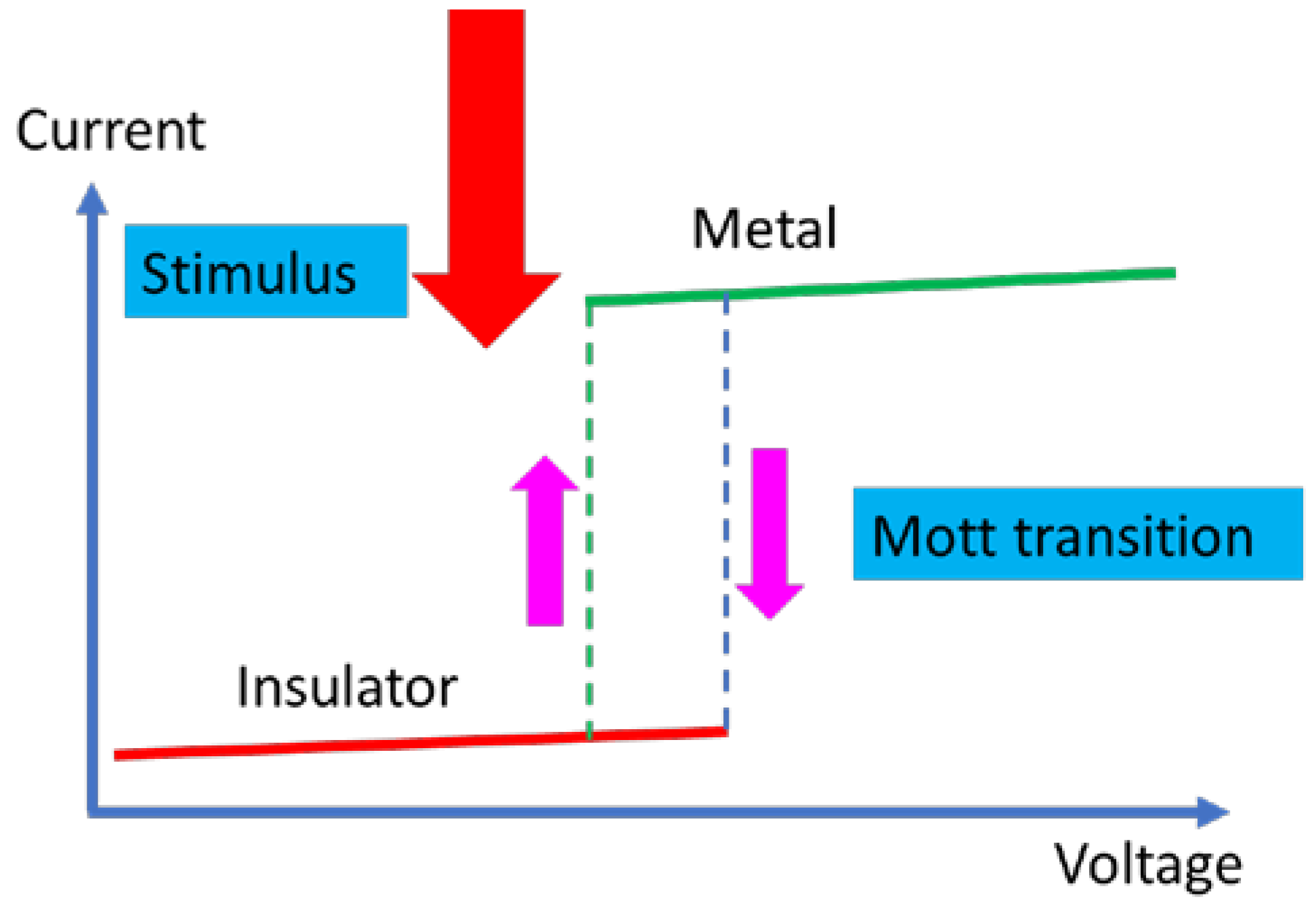
1. Introduction
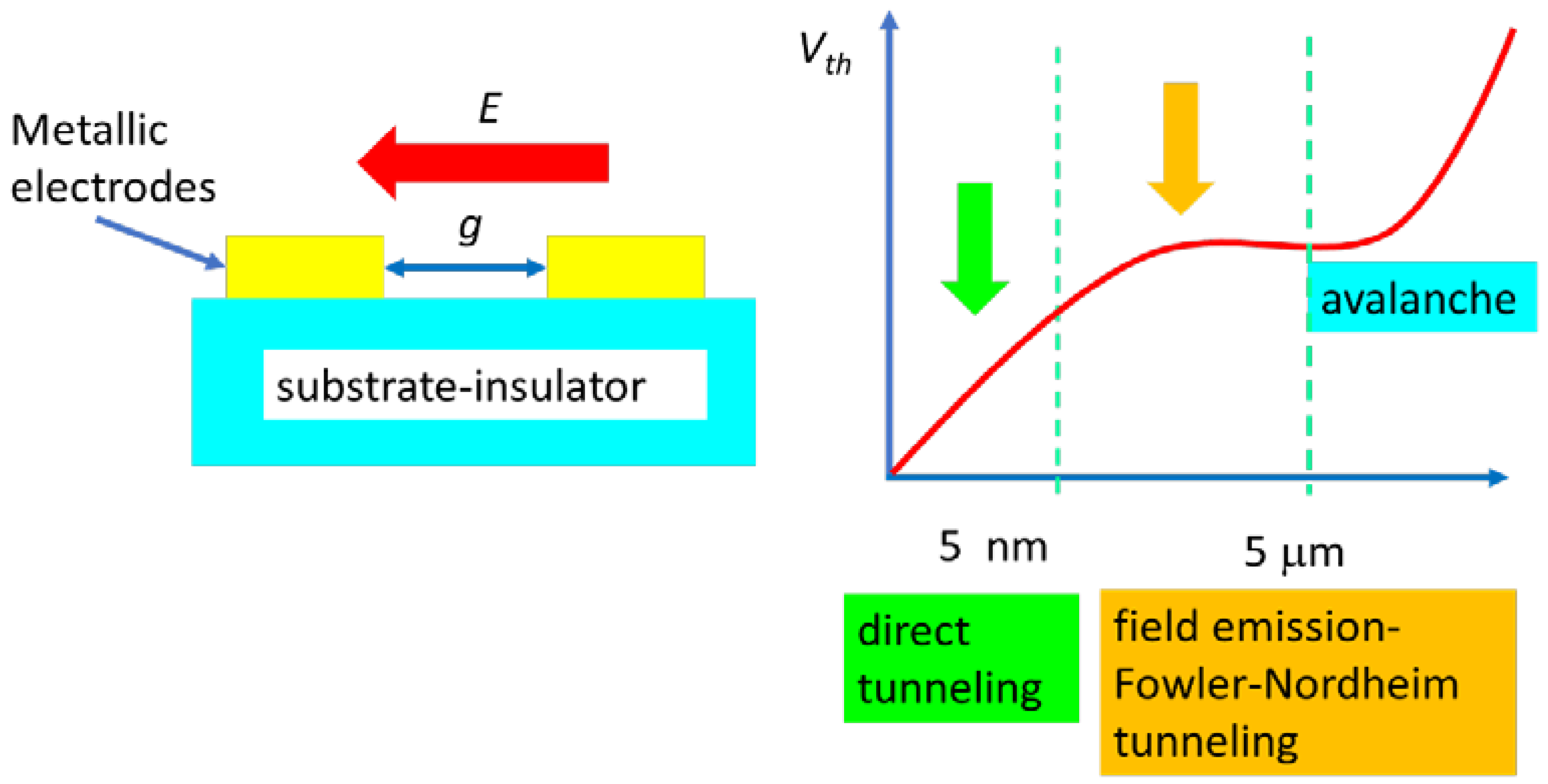
2. Nanoelectronics Devices Based on Electrically Driven MIT
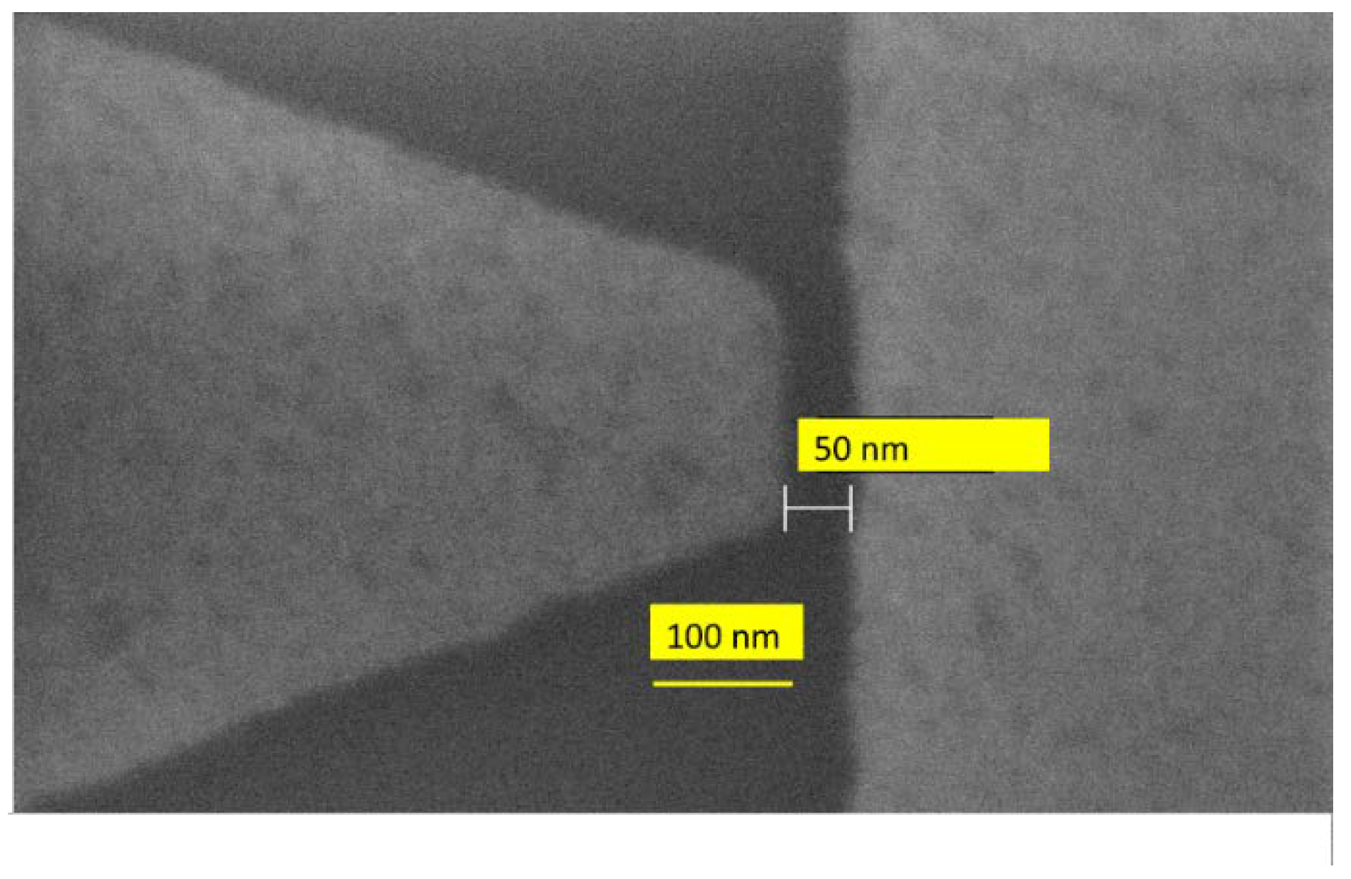
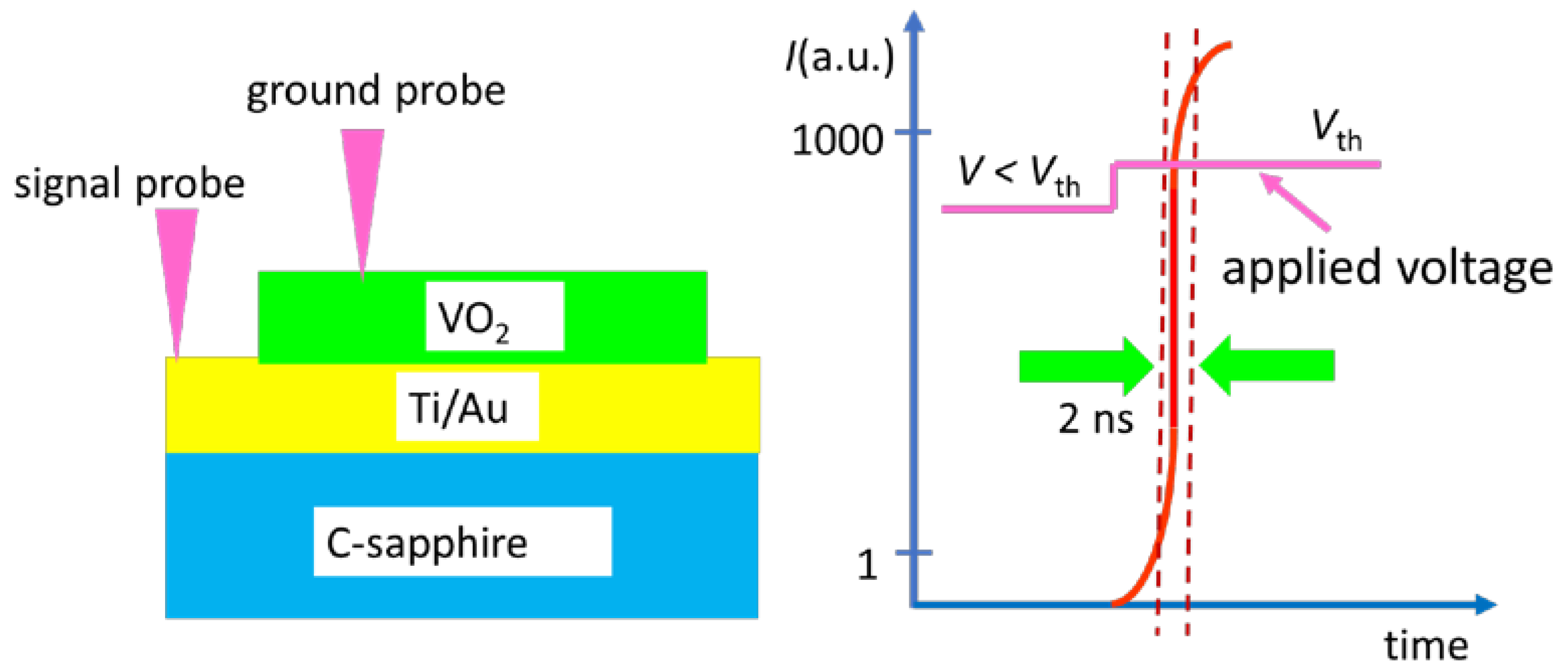
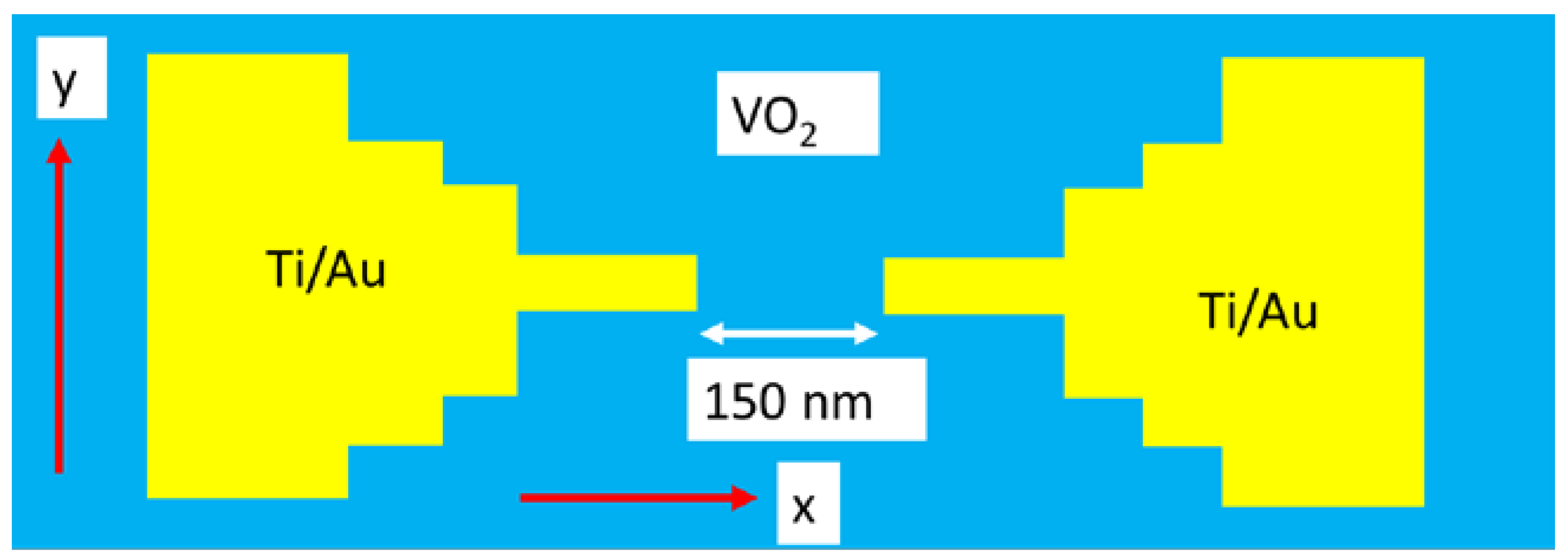
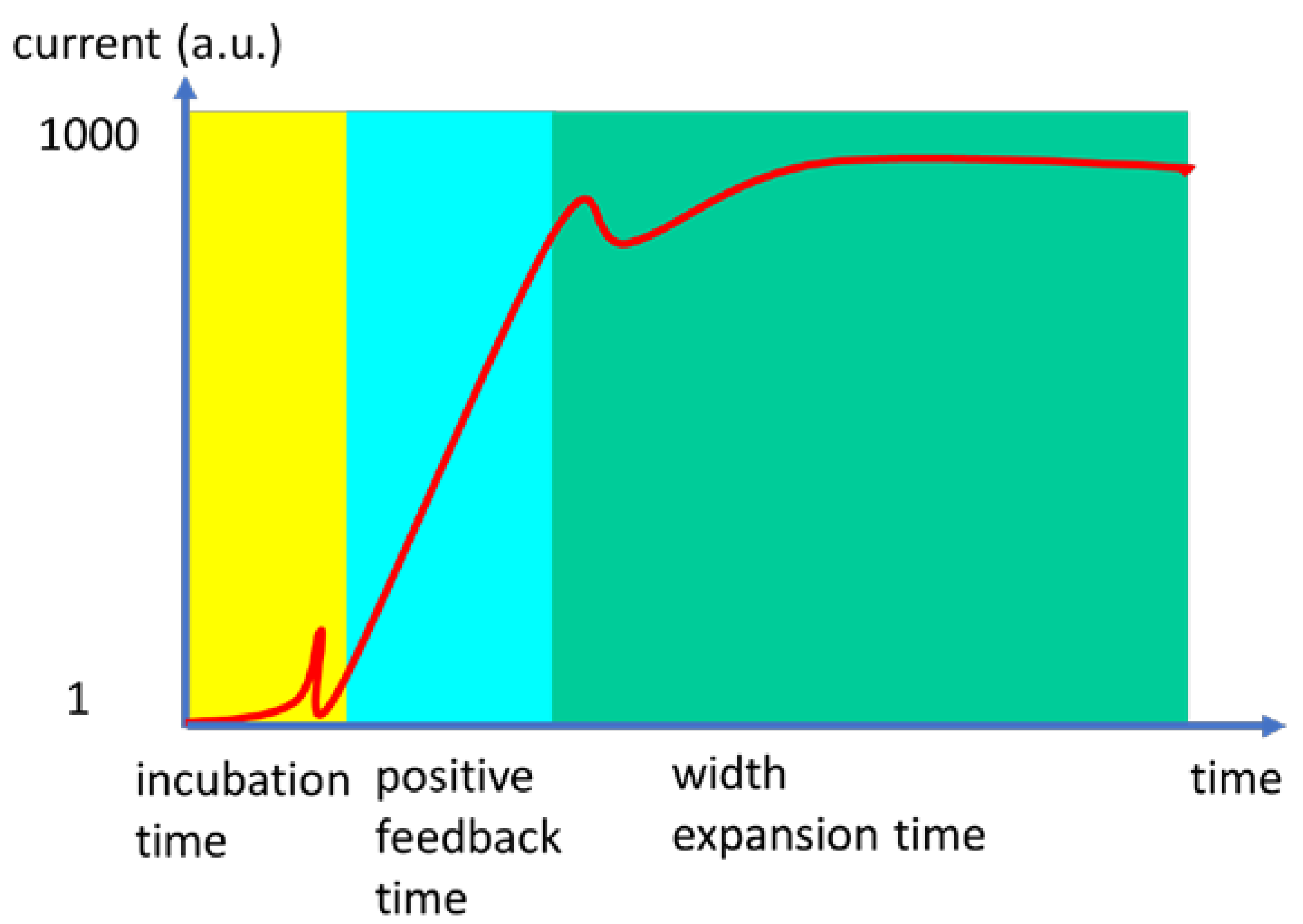
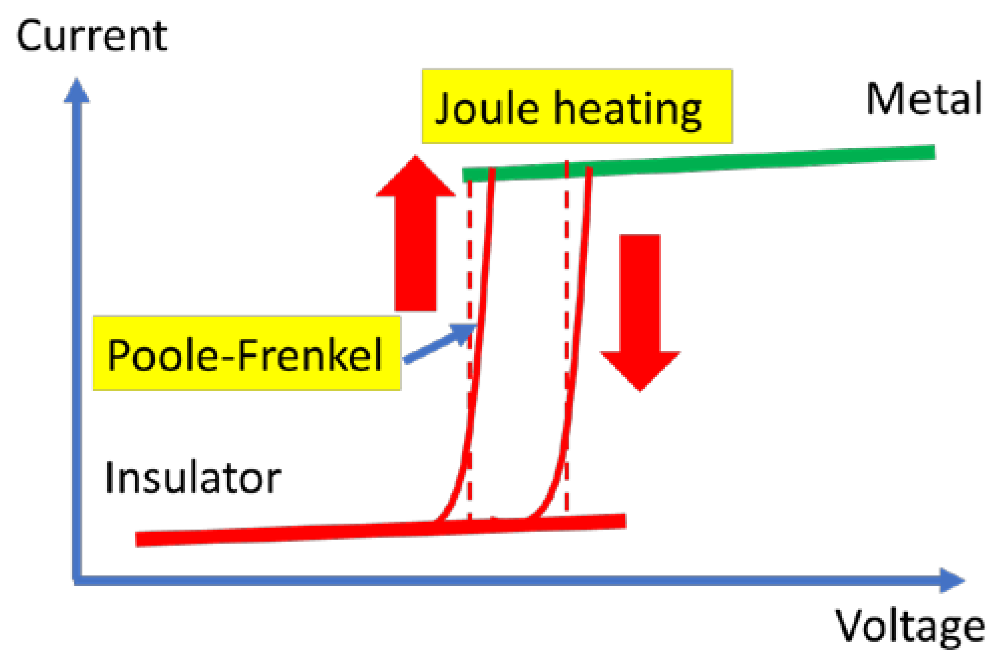
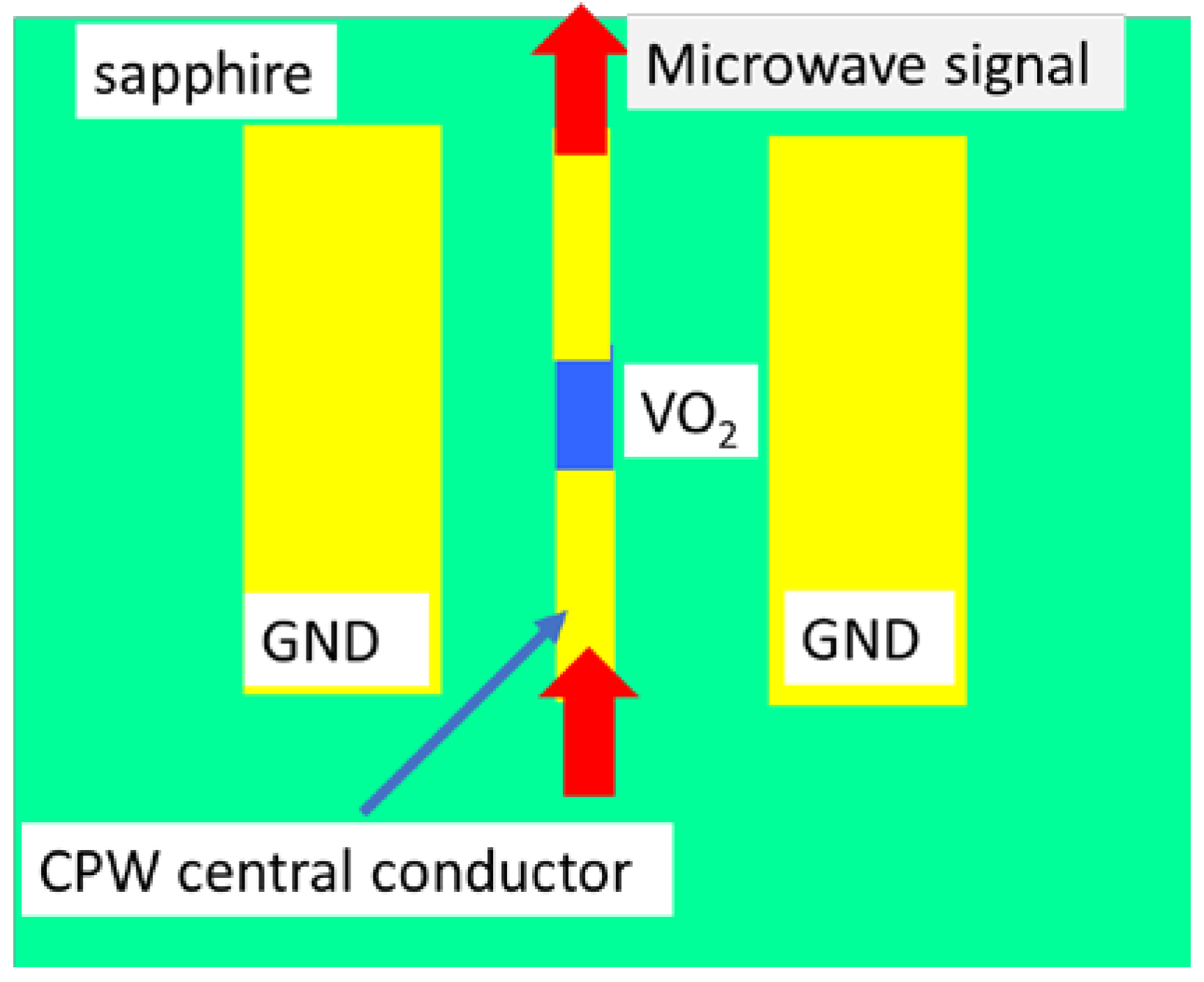
2.1. Ultrafast Nanoelectronics Switches Based on Electrically Driven MIT
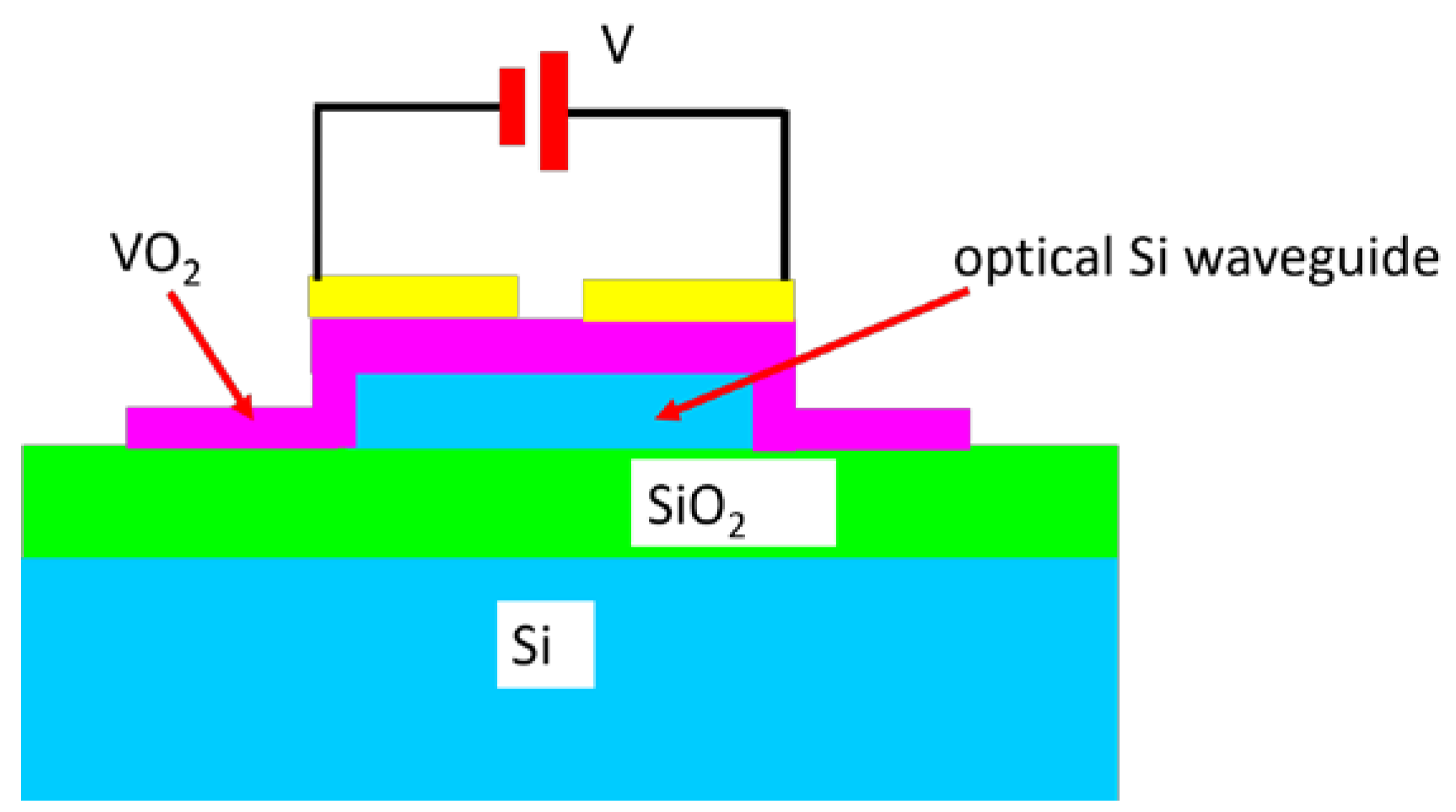
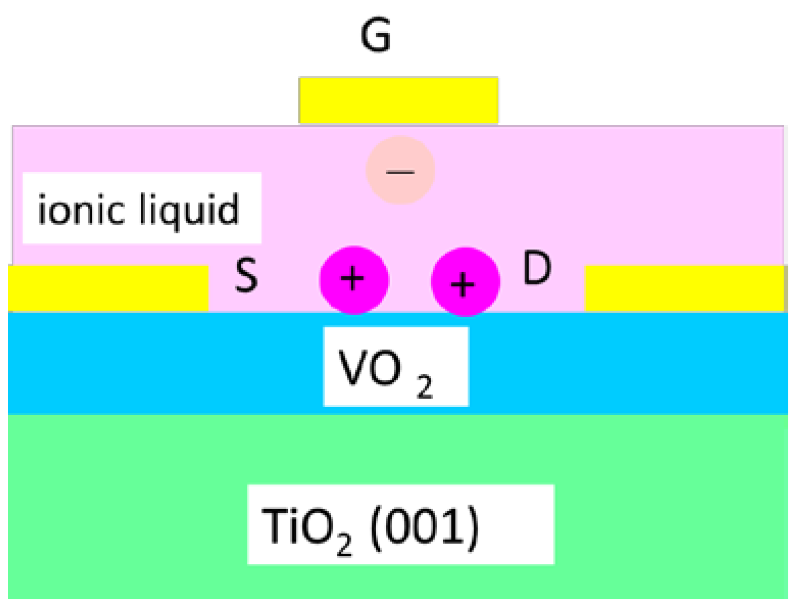
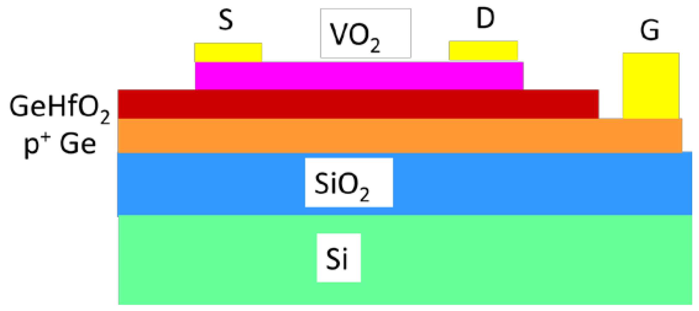
2.2. Nanoelectronics Devices Based on Electrically Driven MIT for Low-Power Applications and Computing
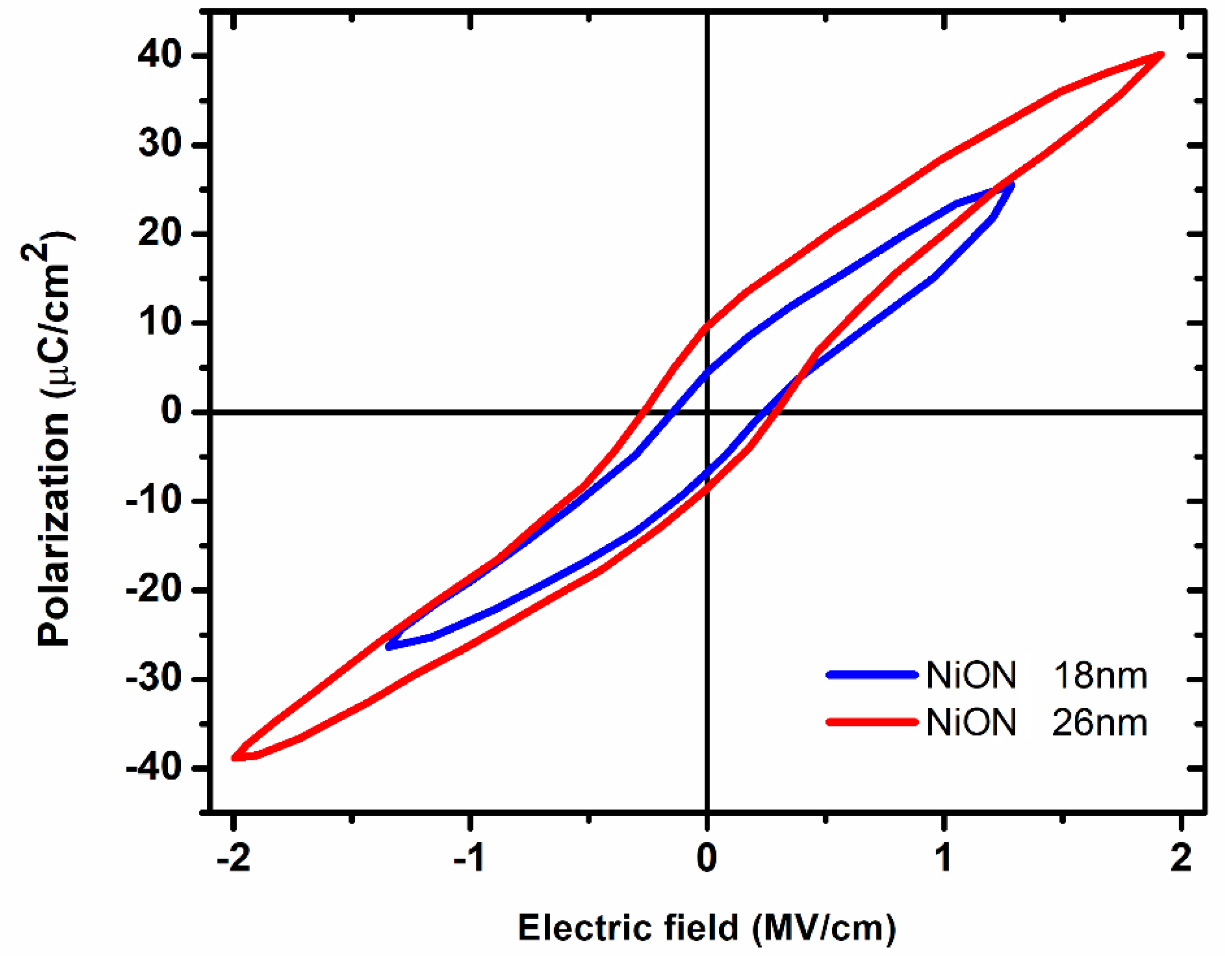
3. New Materials for Electrically Driven MIT
4. Conclusions
Funding
Conflicts of Interest
References
- Yang, Z.; Ko, C.; Ramanathan, S. Oxide electronics utilizing ultrafast metal-insulator transitions. Annu. Rev. Mater. Res. 2011, 41, 337–367. [Google Scholar] [CrossRef]
- Mott, N.F. Metal-insulator transitions. Rev. Mod. Phys. 1968, 40, 677–683. [Google Scholar] [CrossRef]
- Imada, M.; Fujimori, A.; Tokura, Y. Metal-insulator transitions. Rev. Mod. Phys. 1998, 70, 1039–1263. [Google Scholar]
- Milloch, A.; Fabrizio, M.; Giann, C. Mott materials: Unsuccessful metals with a bright future. NPJ Spintron. 2024, 2, 49. [Google Scholar] [CrossRef]
- Evers, F.; Mirlin, A.D. The Andreson transitions. Rev. Mod. Phys. 2008, 80, 1355–1417. [Google Scholar] [CrossRef]
- Segev, M.; Silberberg, Y.; Christodoulides, D.N. Anderson localization of light. Nat. Photon. 2013, 7, 197–203. [Google Scholar] [CrossRef]
- Dragoman, M.; Dragoman, D. The Electronics at Atomic Scale Beyond CMOS; Springer: Cham, Switzerland, 2021. [Google Scholar]
- Cao, W.; Bu, H.; Vinet, M.; Cao, M.; Takagi, S.; Hwang, S.; Ghani, T.; Banerjee, K. The future transistors. Nature 2023, 620, 501–515. [Google Scholar] [CrossRef]
- Liou, J.J.; Ziegler, M.; Schwierz, F. Gigahertz and terahertz transistors for 5G, 6G, and beyond mobile communication systems. Appl. Phys. Rev. 2024, 11, 031318. [Google Scholar] [CrossRef]
- Pavlidis, D. Fundamentals of Terahertz Devices and Applications; Wiley: Hoboken, NJ, USA, 2021. [Google Scholar]
- Nikoo, M.S.; Jafari, A.; Perera, N.; Zhu, M.; Santoruvo, G.; Matioli, E. Nanoplasma-enabled picosecond switches for ultrafast electronics. Nature 2020, 579, 534–539. [Google Scholar] [CrossRef]
- Li, N.; Zhang, B.; He, Y.; Luo, Y. Sub-picosecond nanodiodes for low power ultrafast electronics. Adv. Mater. 2021, 33, 2100874. [Google Scholar] [CrossRef]
- Zhang, P.; Ang, Y.S.; Garner, A.L.; Valfells, Á.; Luginsland, J.W.; Ang, L.K. Space–charge limited current in nanodiodes: Ballistic, collisional, and dynamical effects. Appl. Phys. 2021, 129, 100902. [Google Scholar] [CrossRef]
- Li, Y.; Ang, L.K.; Xiao, B.; Djurabekova, F.; Cheng, Y.; Meng, G. Review of electron emission and electrical breakdown in nanogaps. Phys. Plasmas 2024, 31, 040502. [Google Scholar] [CrossRef]
- Chen, B.; Fan, L.; Bi, J.; Li, Z.; Xu, Z.; Majumdar, S. Nanoscale air channel devices- inheritance and breakthrough of vacuum tube. Nano Mater. Sci. 2024, 6, 714–725. [Google Scholar] [CrossRef]
- Yang, J.H.; Shin, J.H.; Kim, S.; Pyo, G.; Jang, A.-R.; Yang, H.W.; Kang, D.J.; Jang, J.E. Geometrically Enhanced Graphene Tunneling Diode With Lateral Nano-Scale Gap. IEEE Electron Device Lett. 2019, 40, 1840–1844. [Google Scholar] [CrossRef]
- Dragoman, M.; Dinescu, A.; Aldrigo, M.; Dragoman, D. Quantum Graphene Asymmetric Devices for Harvesting Electromagnetic Energy. Nanomaterials 2024, 14, 1114. [Google Scholar] [CrossRef] [PubMed]
- Chai, Z.; Hu, X.; Wang, F.; Niu, X.; Xie, J.; Gong, Q. Ultrafast all-optical switching. Opt. Mater. 2017, 5, 1600665. [Google Scholar] [CrossRef]
- Hassan, M.T. Lightwave Electronics: Attosecond Optical Switching. ACS Photonics 2024, 11, 334–338. [Google Scholar] [CrossRef]
- Lee, Y.J.; Kim, Y.; Gim, H.; Hong, K.; Jang, H.W. Nanoelectronics Using Metal–Insulator Transition. Adv. Mater. 2023, 36, e2305353. [Google Scholar] [CrossRef]
- Zhou, Y.; Ramanathan, S. Mott Memory and Neuromorphic Devices. Proc. IEEE 2015, 103, 1289–1310. [Google Scholar] [CrossRef]
- Bhupathi, S.; Wang, S.; Ke, Y.; Long, Y. Recent progress in vanadium dioxide: The multi-stimuli responsive material and its applications. Mater. Sci. Eng. R Rep. 2023, 155, 100747. [Google Scholar] [CrossRef]
- Hu, P.; Hu, P.; Vu, T.D.; Li, M.; Wang, S.; Ke, Y.; Zeng, X.; Mai, L.; Long, Y. Vanadium Oxide: Phase Diagrams, Structures, Synthesis, and Applications. Chem. Rev. 2023, 123, 4353–4415. [Google Scholar] [CrossRef] [PubMed]
- Zhou, Y.; Chen, X.; Ko, C.; Yang, Z.; Mouli, C.; Ramanathan, S. Voltage-Triggered Ultrafast Phase Transition in Vanadium Dioxide Switches. IEEE Electron Device Lett. 2013, 34, 220–222. [Google Scholar] [CrossRef]
- Rathi, S.; Park, J.-H.; Lee, I.-Y.; Baik, J.M.; Yi, K.S.; Kim, G.-H. Unravelling the switching mechanisms in electric field induced insulator–metal transitions in VO2nanobeams. J. Phys. D Appl. Phys. 2014, 47, 295101. [Google Scholar] [CrossRef]
- Lin, J.; Ramanathan, S.; Guha, S. Electrically Driven Insulator–Metal Transition-Based Devices—Part II: Transient Characteristics. IEEE Trans. Electron Devices 2018, 65, 3989–3994. [Google Scholar] [CrossRef]
- Brockman, J.S.; Gao, L.; Hughes, B.; Rettner, C.T.; Samant, M.G.; Roche, K.P.; Parkin, S.S.P. Subnanosecond incubation times for electric-field-induced metallization of a correlated electron oxide. Nat. Nanotechnol. 2014, 9, 453–457. [Google Scholar] [CrossRef]
- Kalcheim, Y.; Camjayi, A.; del Valle, J.; Salev, P.; Rozenberg, M.; Schuller, I.K. Non-thermal resistive switching in Mott insulator nanowires. Nat. Commun. 2020, 11, 2985. [Google Scholar] [CrossRef]
- Singh, T.; Hummel, G.; Vaseem, M.; Shamim, A. Recent Advancements in Reconfigurable mmWave Devices Based on Phase-Change and Metal Insulator Transition Materials. IEEE J. Microw. 2023, 3, 827–851. [Google Scholar] [CrossRef]
- Jeong, Y.-G.; Bernien, H.; Kyoung, J.-S.; Park, H.-R.; Choi, J.-W.; Kim, B.-J.; Kim, H.-T.; Ahn, K.J.; Kim, D.-S. Electrical control of terahertz nano antennas on VO2 thin film. Opt. Express 2011, 19, 21211. [Google Scholar] [CrossRef]
- Liu, M.; Wei, R.; Taplin, J.; Zhang, W. Terahertz Metasurfaces Exploiting the Phase Transition of Vanadium Dioxide. Materials 2023, 16, 7106. [Google Scholar] [CrossRef]
- Xu, R.; Liu, X.; Lin, Y.-S. Tunable ultra-narrowband terahertz perfect absorber by using metal-insulator-metal microstructures. Results Phys. 2019, 13, 102176. [Google Scholar] [CrossRef]
- Liu, M.; Hwang, H.Y.; Tao, H.; Strikwerda, A.C.; Fan, K.; Keiser, G.R.; Sternbach, A.J.; West, K.G.; Kittiwatanakul, S.; Lu, J.; et al. Terahertz-field-induced insulator-to-metal transition in vanadium dioxide metamaterial. Nature 2012, 487, 345–348. [Google Scholar] [CrossRef] [PubMed]
- Cueff, S.; John, J.; Zhang, Z.; Parra, J.; Sun, J.; Orobtchouk, R.; Ramanathan, S.; Sanchis, P. VO2 nanophotonics. APL Photon. 2020, 5, 110901. [Google Scholar] [CrossRef]
- Jeyaselvan, V.; Pal, A.; Kumar, P.S.A.; Selvaraja, S.K. Thermally-induced optical modulation in a vanadium dioxide-on-silicon waveguide. OSA Contin. 2020, 3, 132–142. [Google Scholar] [CrossRef]
- Markov, P.; Marvel, R.E.; Conley, H.J.; Miller, K.J.; Haglund, R.F., Jr.; Weiss, S.M. Optically Monitored Electrical Switching in VO2. ACS Photonics 2015, 2, 1175–1182. [Google Scholar] [CrossRef]
- Ha, S.D.; Zhou, Y.; Fisher, C.J.; Ramanathan, S.; Treadway, J.P. Electrical switching dynamics and broadband microwave characteristics of VO2 radio frequency devices. J. Appl. Phys. 2013, 113, 184501. [Google Scholar] [CrossRef]
- Kim, Y.; Wu, P.C.; Sokhoyan, R.; Mauser, K.A.; Glaudell, R.; Shirmanesh, G.K.; Atwater, H.A. Phase Modulation with Electrically Tunable Vanadium Dioxide Phase-Change Metasurfaces. Nano Lett. 2019, 19, 3961–3968. [Google Scholar] [CrossRef]
- Azad, S.; Gajula, D.; Prio, M.H.; Muthusamy, L.; Miller, J.K.; Johnson, E.G.; Koley, G. VO2 Thin Film Enabled Free Space Modulation of Infrared Light Using Pulsed Electric Field. ACS Photonics 2024, 11, 2138–2149. [Google Scholar] [CrossRef]
- Jung, Y.; Han, H.; Sharma, A.; Jeong, J.; Parkin, S.S.P.; Poon, J.K.S. Integrated hybrid VO2−silicon optical memory. ACS Photonics 2022, 9, 217–223. [Google Scholar] [CrossRef]
- Cristoloveanu, S.; Wan, J.; Zaslavsky, A. A Review of Sharp-Switching Devices for Ultra-Low Power Applications. IEEE J. Electron Devices Soc. 2016, 4, 215–226. [Google Scholar] [CrossRef]
- Newns, D.M.; Misewich, J.A.; Tsuei, C.C.; Gupta, A.; Scott, B.A.; Schrott, A. Mott transition field effect transistor. Appl. Phys. Lett. 1998, 73, 780–782. [Google Scholar] [CrossRef]
- Hormoz, S.; Ramanathan, S. Limits on vanadium oxide Mott metal–insulator transition field-effect transistors. Solid-State Electron. 2010, 54, 654–659. [Google Scholar] [CrossRef]
- Nakano, M.; Shibuya, K.; Okuyama, D.; Hatano, T.; Ono, S.; Kawasaki, M.; Iwasa, Y.; Tokura, Y. Collective bulk carrier delocalization driven by electrostatic surface charge accumulation. Nature 2012, 487, 459–462. [Google Scholar] [CrossRef]
- Ko, E.; Shin, J.; Shin, C. Steep switching devices for low power applications: Negative differential capacitance/resistance field effect transistors. Nano Converg. 2018, 5, 2. [Google Scholar] [CrossRef] [PubMed]
- Qin, L.; Tian, H.; Li, C.; Xie, Z.; Wei, Y.; Li, Y.; He, J.; Yue, Y.; Ren, T. Steep Slope Field Effect Transistors Based on 2D Materials. Adv. Electron. Mater. 2024, 10, 2300625. [Google Scholar] [CrossRef]
- Shukla, N.; Thathachary, A.V.; Agrawal, A.; Paik, H.; Aziz, A.; Schlom, D.G.; Gupta, S.K.; Engel-Herbert, R.; Datta, S. A steep-slope transistor based on abrupt electronic phase transition. Nat. Commun. 2015, 6, 7812. [Google Scholar] [CrossRef]
- Dragoman, M.; Dragoman, D. Negative differential resistance in novel nanoscale devices. Solid-State Electron. 2022, 197, 108464. [Google Scholar] [CrossRef]
- Frougier, J.; Shukla, N.; Deng, D.; Jerry, M.; Aziz, A.; Liu, L.; Lavallee, G.; Mayer, T.S.; Gupta, S.; Datta, S. Phase-transition-FET exhibiting steep switching slope of 8mV/decade and 36% enhanced on current. In Proceedings of the 2016 IEEE Symposium on VLSI Technology, Honolulu, HI, USA, 14–16 June 2016; pp. 1–2. [Google Scholar] [CrossRef]
- Verma, A.; Song, B.; Downey, B.; Wheeler, V.D.; Meyer, D.J.; Xing, H.G.; Jena, D. Steep Sub-Boltzmann Switching in AlGaN/GaN Phase-FETs With ALD VO2. IEEE Trans. Electron Devices 2018, 65, 945–949. [Google Scholar] [CrossRef]
- Ahn, C.H.; Triscone, J.-M.; Mannhart, J. Electric field effect in correlated oxide systems. Nature 2003, 424, 1015–1018. [Google Scholar] [CrossRef]
- Yamada, H.; Marinova, M.; Altuntas, P.; Crassous, A.; Bégon-Lours, L.; Fusil, S.; Jacquet, E.; Garcia, V.; Bouzehouane, K.; Gloter, A.; et al. Ferroelectric control of a Mott insulator. Sci. Rep. 2013, 3, 2834. [Google Scholar] [CrossRef]
- Dragoman, M.; Aldrigo, M.; Dragoman, D.; Iordanescu, S.; Dinescu, A.; Modreanu, M. HfO2-based ferroelectrics applications in nanoelectronics. Phys. Status Solidi (RRL)–Rapid Res. Lett. 2021, 15, 2000521. [Google Scholar] [CrossRef]
- Silva, J.P.B.; Alcala, R.; Avci, U.E.; Barrett, N.; Bégon-Lours, L.; Borg, M.; Byun, S.; Chang, S.-C.; Cheong, S.-W.; Choe, D.-H.; et al. Roadmap on ferroelectric hafnia- and zirconia-based materials and devices. APL Mater. 2023, 11, 089201. [Google Scholar] [CrossRef]
- Dragoman, M.; Aldrigo, M.; Dragoman, D.; Iordanescu, S.; Dinescu, A.; Vulpe, S.; Modreanu, M. Ferroelectrics at the nanoscale: Materials and devices—A critical review. Crit. Rev. Solid State Mater. Sci. 2022, 48, 561–579. [Google Scholar] [CrossRef]
- Yajima, T.; Nishimura, T.; Tanaka, T.; Uchida, K.; Toriumi, A. Modulation of VO2 metal-insulator- transition by ferroelectric HfO2 gate insulator. Adv. Electron. Mater. 2020, 6, 1901356. [Google Scholar] [CrossRef]
- Vaidya, J.; Kanthi, R.S.S.; Alam, S.; Amin, N.; Aziz, A.; Shukla, N. A three-terminal non-volatile ferroelectric switch with an insulator–metal transition channel. Sci. Rep. 2022, 12, 2199. [Google Scholar] [CrossRef]
- Hao, Y.; Chen, X.; Zhang, L.; Han, M.-G.; Wang, W.; Fang, Y.-W.; Chen, H.; Zhu, Y.; Hong, X. Record high room temperature resistance switching in ferroelectric-gated Mott transistors unlocked by interfacial charge engineering. Nat. Commun. 2023, 14, 8247. [Google Scholar] [CrossRef]
- Loizos, M.; Rogdakis, K.; Parambil, A.P.; Lira-Cantu, M.; Kymakis, E. Emerging materials for resistive switching memories: Prospects for enhanced sustainability and performance for targeted applications. APL Energy 2024, 2, 040901. [Google Scholar] [CrossRef]
- Kim, D.; Yang, S.J.; Wainstein, N.; Skrzypczak, S.; Ducournau, G.; Pallecchi, E.; Happy, H.; Yalon, E.; Kim, M.; Akinwande, D. Emerging memory electronics for non-volatile radiofrequency switching technologies. Nat. Rev. Electr. Eng. 2024, 1, 10–23. [Google Scholar] [CrossRef]
- Zhu, J.; Zhang, T.; Yang, Y.; Huang, R. A comprehensive review on emerging artificial neuromorphic devices. Appl. Phys. Rev. 2020, 7, 011312. [Google Scholar]
- Wang, Y.; Kang, K.-M.; Kim, M.; Lee, H.-S.; Waser, R.; Wouters, D.; Dittmann, R.; Yang, J.J.; Park, H.-H. Mott-transition-based RRAM. Mater. Today 2019, 28, 63–80. [Google Scholar] [CrossRef]
- Ran, Y.; Pei, Y.; Zhou, Z.; Wang, H.; Sun, Y.; Wang, Z.; Hao, M.; Zhao, J.; Chen, J.; Yan, X. A review of Mott insulator in memristors: The materials, characteristics, applications for future computing systems and neuromorphic computing. Nano Res. 2022, 16, 1165–1182. [Google Scholar] [CrossRef]
- Zhao, Z.; Luan, W.; Zhai, Y.; Lv, Z.; Zhang, M.; Yan, Y.; Xue, S.; Zhou, K.; Ding, G.; Han, S.; et al. Mott Memristors for Neuromorphics. Adv. Phys. Res. 2024, 4, 2400129. [Google Scholar] [CrossRef]
- Taha, M.; Walia, S.; Ahmed, T.; Headland, D.; Withayachumnankul, W.; Sriram, S.; Bhaskaran, M. Insulator–metal transition in substrate-independent VO2 thin film for phase-change devices. Sci. Rep. 2017, 7, 17899. [Google Scholar] [CrossRef]
- Mott, N.F. The basis of the electron theory of metals, with special reference to the transition of metals. Proc. Phys. Society Ser. A 1949, 62, 416–422. [Google Scholar] [CrossRef]
- Carlos, E.; Branquinho, R.; Martins, R.; Kiazadeh, A.; Fortunato, E. Recent Progress in Solution-Based Metal Oxide Resistive Switching Devices. Adv. Mater. 2020, 33, e2004328. [Google Scholar] [CrossRef] [PubMed]
- Li, Y.; Wang, Z.; Midya, R.; Xia, Q.; Yang, J.J. Review of memristor devices in neuromorphic computing: Materials sciences and device challenges. J. Phys. D Appl. Phys. 2018, 51, 503002. [Google Scholar] [CrossRef]
- Fumeaux, C.; Herrmann, W.; Kneubuhl, F.K.; Rothuizen, H. Nanometer thin-film Ni–NiO–Ni diodes for detection and mixing of 30 THz radiation. Infrared Phys. Technol. 1998, 39, 123–183. [Google Scholar] [CrossRef]
- Shi, J.; Zhou, Y.; Ramanathan, S. Colossal resistance switching and band gap modulation in a perovskite nickelate by electron doping. Nat. Commun. 2014, 5, 4860. [Google Scholar] [CrossRef]
- Wang, Q.; Puntambekar, A.; Chakrapani, V. Vacancy-Induced Semiconductor–Insulator–Metal Transitions in Nonstoichiometric Nickel and Tungsten Oxides. Nano Lett. 2016, 16, 7067–7077. [Google Scholar] [CrossRef]
- Gavriliuk, A.G.; Trojan, I.A.; Struzhkin, V.V. Insulator-Metal Transition in Highly Compressed NiO. Phys. Rev. Lett. 2012, 109, 086402. [Google Scholar] [CrossRef]
- Dragoman, M.; Vulpe, S.; Aperathithis, E.; Aivalioti, C.; Romanitan, C.; Dinescu, A.; Dragoman, D.; Aldrigo, M.; Djourelov, N.; Modreanu, M.; et al. Oxygen-vacancy induced ferroelectricity in nitrogen-doped nickel oxide. J. Appl. Phys. 2022, 131, 164304. [Google Scholar] [CrossRef]
- Park, D.-S.; Hadad, M.; Riemer, L.M.; Ignatans, R.; Spirito, D.; Esposito, V.; Tileli, V.; Gauquelin, N.; Chezganov, D.; Jannis, D.; et al. Induced giant piezoelectricity in centrosymmetric oxides. Science 2022, 375, 653–657. [Google Scholar] [CrossRef] [PubMed]
- Vulpe, S.; Dragoman, M.; Aldrigo, M.; Nastase, F.; Mladenovic, D.; Ligor, O.; Dragoman, D. Field-effect transistors based on nickel oxide doped with nitrogen semiconductor ferroelectrics for ultralow voltage switch (1 μV), low subthreshold swing and memory. Nanotechnology 2025, 36, 145202. [Google Scholar] [CrossRef]
- Yao, J.; Sun, W.; Guo, J.; Feng, Z.; Pan, Q.; Peng, J.; Cheng, Z.; Dong, S.; Xiong, R.; You, Y. The First Molecular Ferroelectric Mott Insulator. Adv. Mater. 2025, 37, e2414560. [Google Scholar] [CrossRef] [PubMed]
- Dragoman, M.; Modreanu, M.; Sheehan, B.; Vulpe, S.; Romanitan, C.; Aldrigo, M.; Dinescu, A.; Serban, A.B.; Dragoman, D. Field-induced reversible insulator-to-metal transition and the onset of ferroelectricity in molybdenum trioxide films. J. Appl. Phys. 2023, 133, 215101. [Google Scholar] [CrossRef]
- Li, S.; Tian, M.; Gao, Q.; Wang, M.; Li, T.; Hu, Q.; Li, X.; Wu, Y. Nanometre-thin indium tin oxide for advanced high-performance electronics. Nat. Mater. 2019, 18, 1091–1097. [Google Scholar] [CrossRef] [PubMed]
- Alsaif, M.M.Y.A.; Chrimes, A.F.; Daeneke, T.; Balendhran, S.; Bellisario, D.O.; Son, Y.; Field, M.R.; Zhang, W.; Nili, H.; Nguyen, E.P.; et al. High-Performance Field Effect Transistors Using Electronic Inks of 2D Molybdenum Oxide Nanoflakes. Adv. Funct. Mater. 2015, 26, 91–100. [Google Scholar] [CrossRef]
- Liu, A.; Zhang, X.; Liu, Z.; Li, Y.; Peng, X.; Li, X.; Qin, Y.; Hu, C.; Qiu, Y.; Jiang, H.; et al. The Roadmap of 2D Materials and Devices Toward Chips. Nano-Micro Lett. 2024, 16, 119. [Google Scholar] [CrossRef]


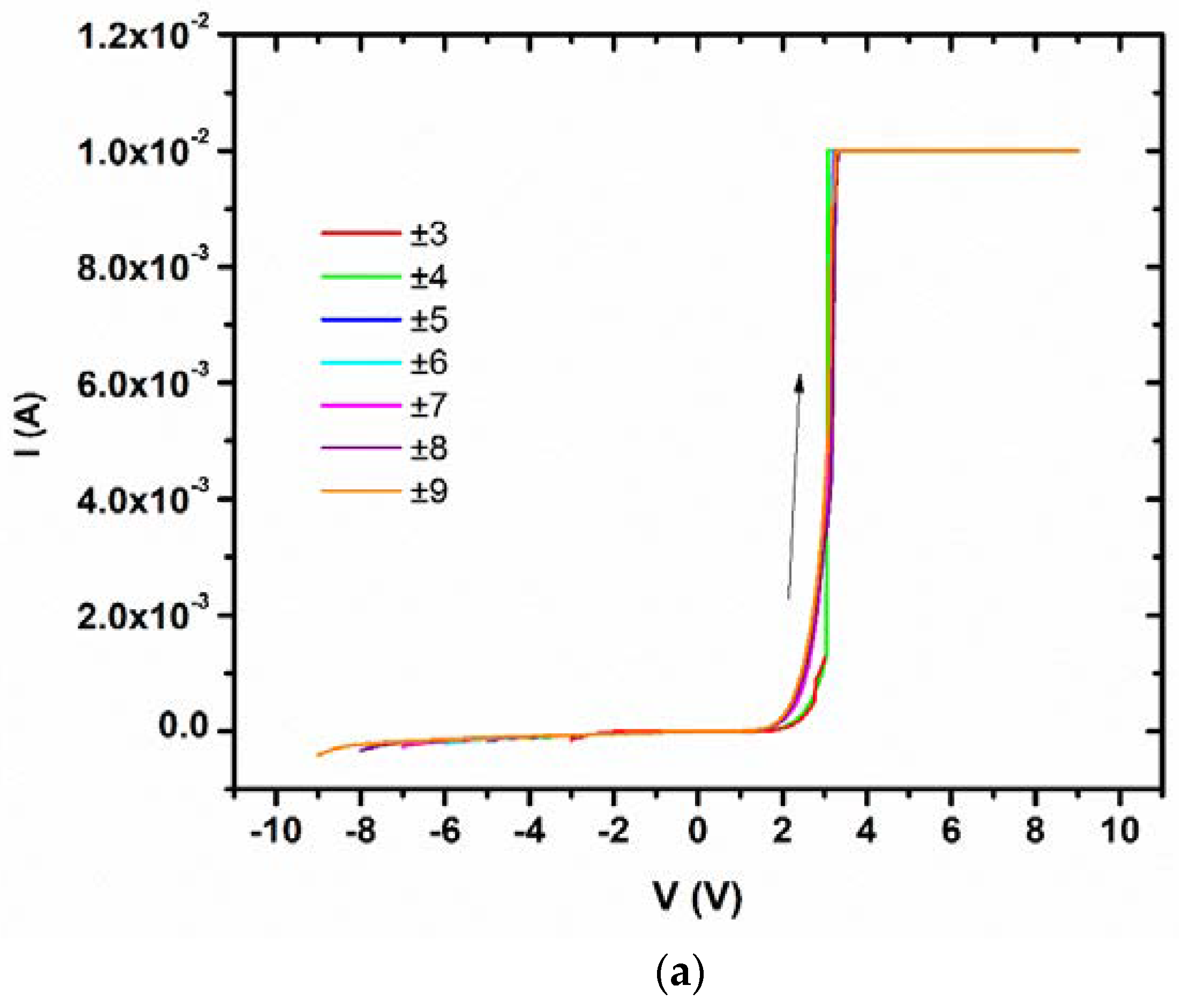
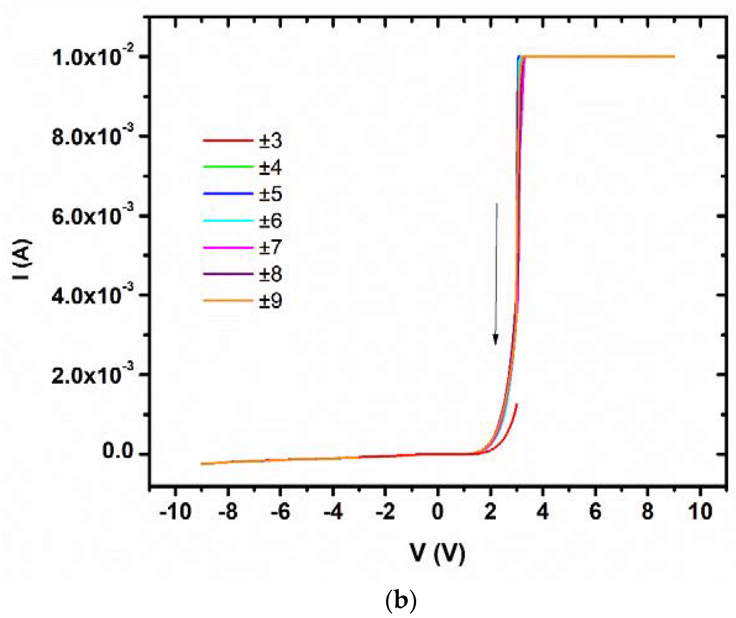
| MoO2.96 Thickness (nm) | Nr. of Measured Devices | Threshold of Phase Transition (V) | Hysteresis Width (V) | SS (mV/Decade) |
|---|---|---|---|---|
| 10 | 18 | 3 | 0.1 | 48.3 |
| 15 | 19 | 5 | 0.1 | 48 |
| 25 | 17 | 2.5 | 0.3 | 48 |
Disclaimer/Publisher’s Note: The statements, opinions and data contained in all publications are solely those of the individual author(s) and contributor(s) and not of MDPI and/or the editor(s). MDPI and/or the editor(s) disclaim responsibility for any injury to people or property resulting from any ideas, methods, instructions or products referred to in the content. |
© 2025 by the authors. Licensee MDPI, Basel, Switzerland. This article is an open access article distributed under the terms and conditions of the Creative Commons Attribution (CC BY) license (https://creativecommons.org/licenses/by/4.0/).
Share and Cite
Dragoman, M.; Dragoman, D.; Modreanu, M.; Vulpe, S.; Romanitan, C.; Aldrigo, M.; Dinescu, A. Electric-Field-Induced Metal-Insulator Transition for Low-Power and Ultrafast Nanoelectronics. Nanomaterials 2025, 15, 589. https://doi.org/10.3390/nano15080589
Dragoman M, Dragoman D, Modreanu M, Vulpe S, Romanitan C, Aldrigo M, Dinescu A. Electric-Field-Induced Metal-Insulator Transition for Low-Power and Ultrafast Nanoelectronics. Nanomaterials. 2025; 15(8):589. https://doi.org/10.3390/nano15080589
Chicago/Turabian StyleDragoman, Mircea, Daniela Dragoman, Mircea Modreanu, Silviu Vulpe, Cosmin Romanitan, Martino Aldrigo, and Adrian Dinescu. 2025. "Electric-Field-Induced Metal-Insulator Transition for Low-Power and Ultrafast Nanoelectronics" Nanomaterials 15, no. 8: 589. https://doi.org/10.3390/nano15080589
APA StyleDragoman, M., Dragoman, D., Modreanu, M., Vulpe, S., Romanitan, C., Aldrigo, M., & Dinescu, A. (2025). Electric-Field-Induced Metal-Insulator Transition for Low-Power and Ultrafast Nanoelectronics. Nanomaterials, 15(8), 589. https://doi.org/10.3390/nano15080589