Article

Photopic Adaptation Mimicked by Y2O3-Based Optoelectronic Memristor for Neuromorphic Visual System

Key Laboratory for UV Light-Emitting Materials and Technology, Northeast Normal University, Ministry of Education, 5268 Renmin Street, Changchun 130024, China
*
Authors to whom correspondence should be addressed.
These authors contributed equally to this work.
Nanomaterials 2025, 15(8), 579; https://doi.org/10.3390/nano15080579
Submission received: 27 February 2025 / Revised: 3 April 2025 / Accepted: 9 April 2025 / Published: 11 April 2025

Abstract

:
Visual adaptation is one of the most significant features that helps organisms process complicated image information in time-varying environments. Emulating this function is highly desirable for energy-efficient image perception. In this work, we demonstrate an yttrium oxide (Y2O3)-based optoelectronic memristor and emulate photopic adaptation behavior in a single device. Decay amplitude and photosensitivity are indexed to describe the time-dependent characteristics of photopic adaptation. An intensity-dependent characteristic, namely Weber’s law, is also investigated in this work. Photopic adaptation originates from the trapping of photogenerated carriers in oxygen vacancies. Based on photopic adaptation behavior, a neuromorphic vision system capable of adapting to environmental brightness is constructed using the proposed optoelectronic memristor array. Memristor arrays can emulate sensing and adaptation functions in order to enhance images against bright backgrounds. Our work provides a feasible pathway toward self-adaptive neuromorphic vision systems.

1. Introduction

Due to the multifunctional integration of image sensing, storage, and processing for next-generation human–machine interactions and humanoid robots [1,2,3,4,5,6,7,8], bio-inspired neuromorphic vision systems have gained considerable attention in recent years. Conventional artificial visual systems are usually composed of different functional units according to their architectural design and manufacturing technologies. A lack of neuromorphic function and the separation of the physical architecture would result in both significant energy consumption and data delay problems [9,10,11]. In contrast, neuromorphic visual systems with an in-sensor computing architecture have considerable potential in highly efficient image perception. The development of a novel neuromorphic visual system is at the cutting edge of research in this field, exhibiting great promise for applications in neuromorphic intelligence technologies and machine vision [11,12,13].
In biological visual systems, the visual adaptation function is an important feature in achieving autonomic responses to environmental stimuli. This ability is beneficial in adapting to varying light environments [14,15,16]. For instance, an individual might experience temporary dizziness due to retinal overstimulation when suddenly exposed to bright light. Then, the retina gradually reduces its sensitivity over time, enabling improved visual perception. The process by which sensitivity gradually decreases under continuous light stimulation is photopic adaptation. Moreover, the perceived change is proportional to the stimuli intensity, which is known as Weber’s law [17,18,19], which is the critical capacity of the organism to identify and distinguish diverse perceptual stimuli from the background. Visual adaptation enables the human eye to perform detailed visual information analysis in a time-varying environment. However, in conventional machine vision systems, the adaptive processing function usually requires complex hardware circuitry and algorithms, which typically limits the operating efficiency [20,21]. Therefore, developing novel neuromorphic hardware to implement these biological adaptabilities is greatly desired for highly efficient visual perception. To date, much effort has been made in constructing optoelectronic devices to demonstrate visual adaptive processing functions [22,23,24,25,26]. He et al. proposed a photo-triggered organic active adaptation transistor (OAAT) and emulated visual active adaptation by combining photovoltaic- and field-effect modulation [23]. The OAAT exhibits excellent stability and uniformity, and this approach can be applied to a wide variety of organic semiconductors. Liao et al. reported a vision sensor array that uses a bottom-gate bilayer MoS2 phototransistor; they demonstrated both scotopic and photopic adaptation by introducing trap states, offering a broad perception range and image contrast enhancement [26].
In this work, we reported a two-terminal memristor with photopic adaptation behaviors by utilizing the nanocomposite film of sodium alginate (SA) and Y2O3 NPs. The time-dependent characteristic of photopic adaptation is investigated by experimentally measuring decay amplitude and photosensitivity (Pt) values. In addition, the intensity-dependent characteristic of visual adaptation, i.e., Weber’s law, is also investigated in this work. The above photopic adaptation can be attributed to the trapping and detrapping behaviors of photogenerated electrons in the Y2O3. Furthermore, an optoelectronic memristor array with photopic adaptation behavior was fabricated, substantially improving the efficiency and accuracy of the image recognition process. The Y2O3-based optoelectronic memristor can be regarded as a promising candidate device for constructing self-adaptive neuromorphic vision systems.

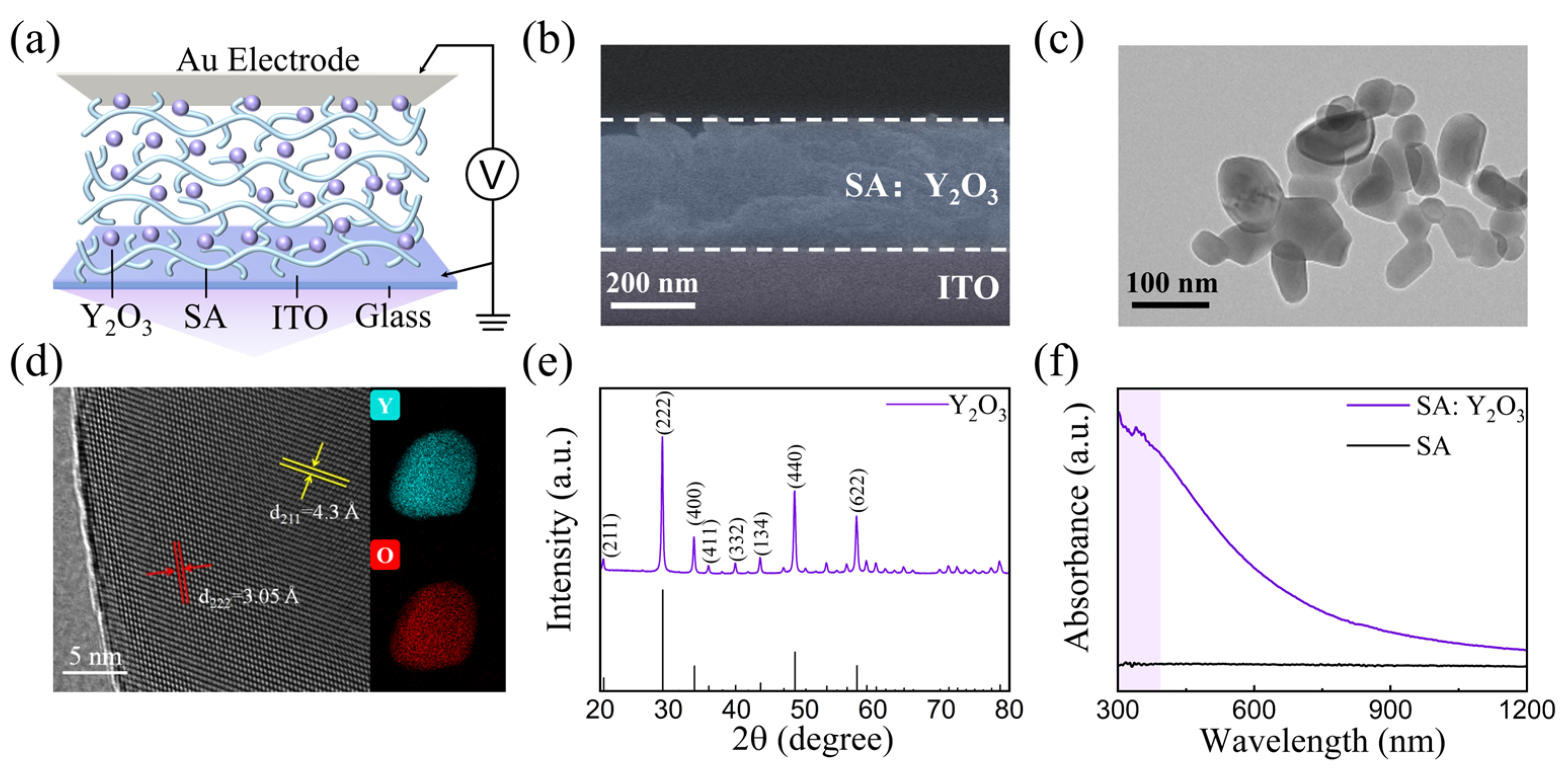
2. Materials and Methods

Device Fabrication:
Memristors with Au/SA: Y2O3 NPs /FTO sandwich structures were fabricated on ITO substrates and then patterned into optoelectronic memristive arrays with a diameter of 500 μm using a metal mask. SA powder and Y2O3 NPs powder was purchased from Macklin Biochemical Co., Ltd., Shanghai, China. First, SA powder (100 mg) and Y2O3 NPs (200 mg) were mixed in deionized water (10 mL). The solution was mechanically stirred at room temperature for a long time (≥3 h), allowing the powder to dissolve fully and the SA: Y2O3 NPs nanocomposite film to be formed. The film was fabricated by spin-coating SA: Y2O3 NPs solutions on the ITO/glass substrate with a spin speed of 3000 rpm and spin time of 30 s. Finally, the Au electrodes were deposited on the top of the film to act as electrodes by using thermal evaporation methods.
Measurement and Characterization:
The optical signals were measured using a xenon lamp (LA-410UV, Hayashi, Tokyo, Japan) with an optical filter. Device conductance was monitored with a source meter (2636b, Keithley, Solon, OH, USA) and a probe station (TTPX, Lake Shore, Westerville, OH, USA). The positive current was defined as the flow from the top Au electrode to the bottom ITO electrode. The Y2O3 nanoparticles in mechanism part were annealed at 500 °C in a muffle furnace under an air atmosphere for 3 h.

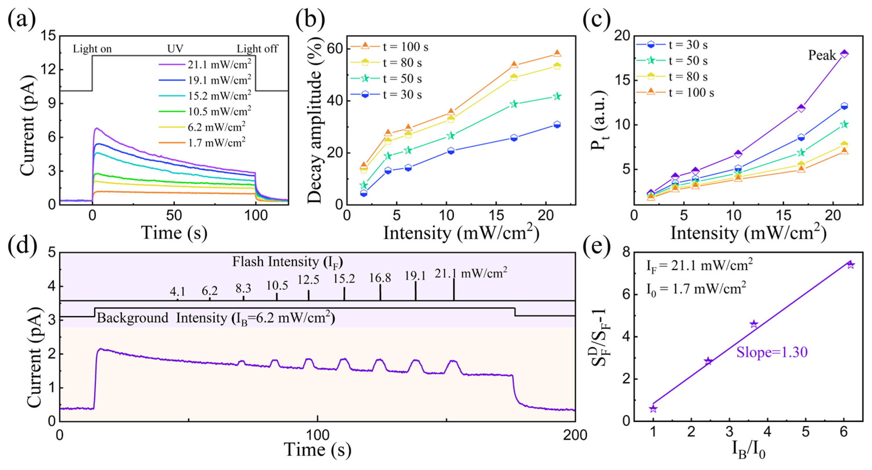
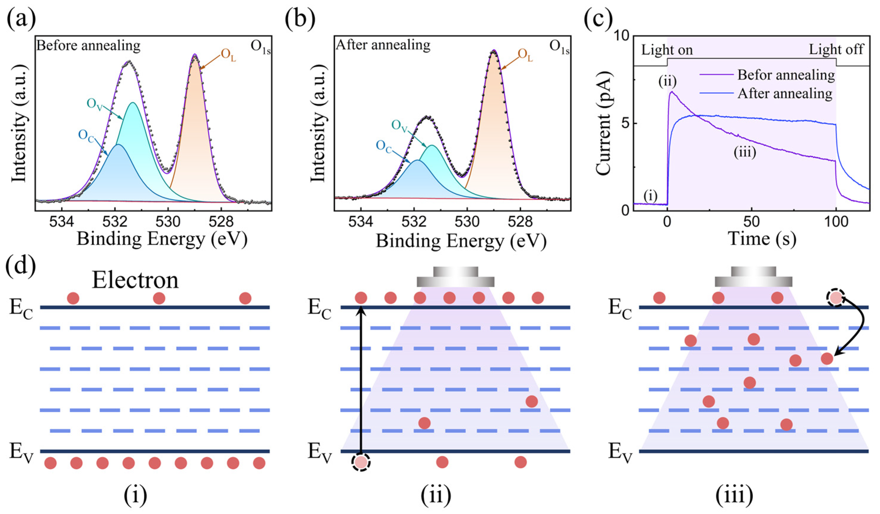
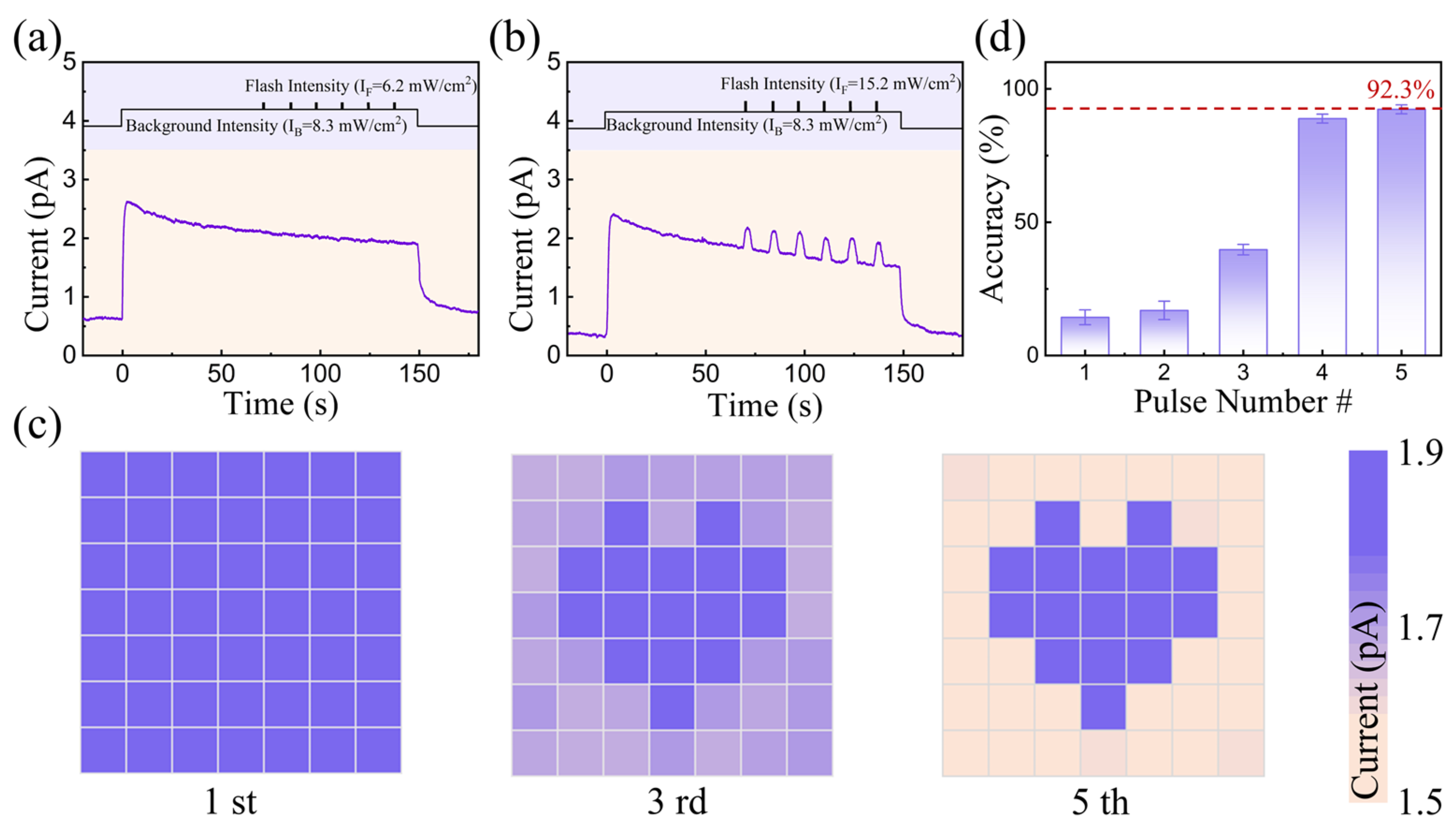
3. Results and Discussion

As shown in Figure 1a, the optoelectronic memristor consists of an Au/SA: Y2O3 NPs/indium tin oxide (ITO) sandwich structure. A cross-sectional scanning electron microscopy (SEM) image of SA: Y2O3 is presented in Figure 1b; the film thickness is about 300 nm. In addition, Au films were deposited using thermal evaporation methods, and these served as the top electrodes (TEs). A read voltage of 0.5 V was applied to the Au top electrode, while the bottom ITO electrode was grounded, and the optical signal was applied to the device through the top electrode. As shown in the transmission electron microscopy (TEM) images (Figure 1c,d), Y2O3 NPs with a spherical shape exhibit an average particle size of ~50 nm. The lattice fringes of 0.430 and 0.305 nm correspond to the (211) and (222) planes of anatase Y2O3, respectively. Then, the crystallographic structure of Y2O3 NPs was uncovered by XRD measurements, as shown in Figure 1e. Y2O3 NPs have eight broad peaks at 20.5°, 29.1°, 33.8°, 35.9°, 39.8°, 43.5°, 48.5°, and 57.6°, corresponding to the (211), (222), (400), (411), (332), (134), (440), and (622) planes, respectively; this is consistent with the cubic phase of Y2O3 [27,28,29]. Figure 1f illustrates the absorbance spectra of SA: Y2O3 NPs nanocomposite and pure SA films. Using the SA film as a reference, the SA: Y2O3 NPs film exhibits strong light absorption at wavelengths smaller than 390 nm [30,31,32]. Therefore, in this work, optical modulation was performed using a xenon lamp with a UV (360–390 nm) optical filter.
As a critical feature of biological retina, visual adaptation comprises two primary forms, i.e., scotopic and photopic adaptation [33,34,35]. In this work, photopic adaptation is implemented using the characteristic that the output current decreases over time under high-intensity UV irradiation. Figure 2a shows the photoresponsivity evolution of our device under different irradiation conditions. In this work, the photocurrent was recorded under a fixed voltage of 0.5 V, contributing to its ultra-low power consumption (pW level). The memristor current exhibits a gradual increase at a light intensity of 1.7 mW/cm2. By contrast, the output current increases initially and then decreases gradually within the following few seconds, when the optical intensity increases to 6.2 mW/cm2. The above process is similar to photopic adaptation in biological visual systems. The devices have excellent uniformity across 50 continuous cycles (Supplementary Material, Figure S1), providing a stable basis for implementing photopic adaptation in future studies. In this case, the time-dependent decay amplitude and photosensitivity (Pt) are defined as follows:
Decay amplitude = (IpeakIt)/Ipeak × 100%
Pt = ΔIt/Idark
where Ipeak represents the transient output current under light stimulus, It is the current after ‘t’ seconds of light irradiation, and Idark is the dark current. Then, we evaluated the photopic adaptation performance after light exposure for ‘t’ seconds (Supplementary Material, Figure S2) [23,36,37]. It can be seen that the decay amplitude increased with an increase in light intensity, as shown in Figure 2b; this is analogous with the photopic adaptation feature. The above result indicates that photopic adaptation is preferentially activated under high-intensity optical stimulus, protecting the receptors from fatigue [37,38]. In addition, as shown in Figure 2c, the photosensitivity after light exposure at 21.1 mW/cm2 for 30, 50, 80, and 100 s decreased from 18 to 12.1, 10.1, 7.6, and 7.0, respectively, consistent with the photopic adaptation feature.
Moreover, Weber’s law is emulated by introducing additional flash stimulations with IF varying from 8.3 to 21.1 mW/cm2, as shown in Figure 2d and Supplementary Material Figure S3. The background intensity IB is desensitized to steady states. It can be seen that the device current is only sensitive to flash stimulation as IF is larger than IB. This means that the device sensitivity of flash stimulation strongly depends on the background condition. The proportional relationship between sensitivity changes and background intensity is known as Weber’s law, which is expressed as follows:
S F D S F 1 = I B I 0
where S F D and SF are the flash sensitivity in darkness and under background conditions, respectively. I0 is equal to the background intensity required to reduce the sensitivity by half [37,38,39]. According to our experimental results (Supplementary Material, Figure S4), the constants S F D and I0 are calculated as 0.1 and 1.7 mW/cm2, respectively. Figure 2e shows the curve of Weber’s law according to Equation (1), where SF is inversely proportional to IB with a slope of 1.30, resembling that of biological receptors.
We also investigated the operating mechanism of our Y2O3-based optoelectronic memristor. According to Figure 1d and Figure 2a, light-induced adaptation behavior can be attributed to the Y2O3 NPs in the nanocomposite film. Generally, the characteristics of oxide films are closely associated with their chemical compositions [40]. X-ray photoelectron spectroscopy (XPS) was used to investigate the surface composition and chemical states of Y2O3 nanoparticles. As shown in Figure 3a,b, the O1s XPS spectra of Y2O3 nanoparticles before and after annealing are fitted into three components. The peaks located at 529.0, 531.3, and 531.8 eV correspond to lattice oxygen (OL), oxygen vacancies (OV), and chemisorbed oxygen (OC), respectively [41,42,43]. A large amount of OV exists in the Y2O3 nanoparticles before annealing; however, after annealing, the amount of OV clearly decreases. Figure 3c shows the responsivity evolution of our device before and after annealing. Before annealing, the response current rises abruptly when the device is irradiated by UV light and then decays gradually, indicating photopic adaptation. By contrast, Au/Y2O3(annealed)/ITO exhibits a gradual increase in response current under the same UV light. These results suggest that the photopic adaptation behavior can be attributed to electron trapping/detrapping in OV. As shown in Figure 3d, upon light irradiation, electrons in the valence band and trap states are promptly excited into the conduction band, accompanied by a synchronously enhanced photocurrent. However, some photogenerated carriers will be captured by the trap sites in Y2O3, causing photocurrent attenuation. Thermal treatment reduces inherent trap sites effectively, thereby reducing the trapping probability of photogenerated electrons. As above, photopic adaptation behavior is absent in annealed devices [44,45,46].
In addition, in our memristive array, image sensing and adaptation behavior under a bright background can be emulated in our memristive array. We constructed a 7 × 7 device array to perceive the ‘heart-shaped’ pattern under a bright light background (Supplementary Material Figure S5); a light stimulus of 8.3 mW/cm2 was applied to all 7 × 7 pixels as a bright background. Light signals with different intensities (6.2 and 15.2 mW/cm2, 2 s) were applied to parts of the units as ‘heart-shaped’ patterns, respectively, as illustrated in Figure 4a,b. For a flash intensity of 6.2 mW/cm2, the ‘heart-shaped’ patterns could not be identified from the bright background conditions (Supplementary Material Figure S6) because the device is only sensitive to flash stimulations, as IF is larger than IB in the photopic adaptation state. For a flash intensity of 15.2 mW/cm2, the device array with a larger response current value was saturated in the instantaneous exposure environment, hindering image recognition. Interestingly, the ‘heart-shaped’ patterns could be gradually identified from the bright background conditions due to the decreased sensitivity under continuous optical irradiation, as shown in Figure 4c. The recognition accuracy of images against bright backgrounds can be improved from 14.34% to 92.32%, with the light pulse number increasing to 5, as shown in Figure 4d. These results indicate that our device can be utilized as exposure control elements for the next generation of intelligent circuits, exhibiting considerable potential for application in artificial intelligence, i.e., autonomous driving, and vision.

4. Conclusions

In summary, we demonstrated a Y2O3-based optoelectronic memristor and emulated the photopic adaptation of biological retina. Moreover, the time-dependent nature of photopic adaptation and the changing sensitivity, dependent on background conditions (i.e., Weber’s law), were also investigated. The corresponding mechanism can be attributed to the trapping of photogenerated electrons in oxygen vacancies. We emulated image sensing and adaptation functions based on photopic adaptation. Our work provides a promising hardware platform for future self-adaptive neuromorphic vision systems and human–machine interfaces.

Supplementary Materials

The following supporting information can be downloaded at: https://www.mdpi.com/article/10.3390/nano15080579/s1, Figure S1: The statistical distribution of the Ipeak and Isteady variability for 50 continuous cycles. Figure S2: Definition of time-dependent photosensitivity (Pt) and Decay amplitude, where Idark is the dark current, It is the current after t seconds of light irradiation and Ipeak represents the under light stimulus. Figure S3: Current response of Y2O3-based optoelectronic memristor to background stimulation (intensity of 1.7 and 4.1 mW/cm2) and flash stimulations (intensity from 4.1 to 21.1 mW/cm2). Figure S4: (a) Current response of Y2O3-based optoelectronic memristor under background stimulation of 0 mW/cm2. (b) Correlation between sensitivity and background intensity. Figure S5: A photograph of a 7 × 7 optoelectronic memristive array with each pixel having an area of ~0.78 mm2. Figure S6: The process of recognizing the ‘heart-shaped’ pattern under a bright background (8.3 mW/cm2) with a flash intensity of 6.2 mW/cm2 in a 7 × 7 device array. With continuous light background, the ‘heart shape’ pattern cannot be identified from the bright background conditions.

Author Contributions

J.S. and S.Q. contributed equally to this work. Conceptualization, J.S., S.Q. and X.S.; data curation, J.S., S.Q. and Z.L. (Zhuangzhuang Li); formal analysis, X.S., Z.L. (Zhuangzhuang Li) and Y.L.; funding acquisition, X.S., Y.T., X.Z., Y.L. and Z.W.; investigation, J.S., S.Q. and Z.L. (Zhuangzhuang Li); methodology, S.Q., Z.L. (Zhipeng Li) and C.W.; resources, Z.L. (Zhipeng Li), C.W., Y.T., X.Z., Y.L. and Z.W.; supervision, Z.L. (Zhipeng Li) and X.Z.; validation, Z.L. (Zhipeng Li), C.W., Y.T. and Z.W.; writing—original draft, J.S. and X.S.; writing—review and editing, Z.L. (Zhuangzhuang Li), C.W., Y.T., X.Z., Y.L. and Z.W. All authors have read and agreed to the published version of the manuscript.

Funding

This study was supported by the NSFC Program (Nos. 52372137, U23A20568, 52472149, 52402175, and 52272140), the “111” Project (No. B13013), the China Postdoctoral Science Foundation (GZB20240135), the Jilin Province Education Foundation (JJKH20211278KJ), and the Fundamental Research Funds for the Central Universities (No. 2412025QC001, 2412023YQ004).

Data Availability Statement

The data that support the findings of this study are available from the corresponding authors upon reasonable request.

Conflicts of Interest

The authors declare no conflicts of interest.

References

  1. Zhu, Q.; Li, B.; Yang, D.; Liu, C.; Feng, S.; Chen, M.; Sun, Y.; Tian, Y.; Su, X.; Wang, X.; et al. A flexible ultrasensitive optoelectronic sensor array for neuromorphic vision systems. Nat. Commun. 2021, 12, 1798. [Google Scholar] [CrossRef] [PubMed]
  2. Kim, M.S.; Kim, M.S.; Lee, G.J.; Sunwoo, S.H.; Chang, S.; Song, Y.M.; Kim, D.H. Bio-Inspired Artificial Vision and Neuromorphic Image Processing Devices. Adv. Mater. Technol. 2022, 7, 2100144. [Google Scholar] [CrossRef]
  3. Choi, C.; Lee, G.J.; Chang, S.; Song, Y.M.; Kim, D.H. Inspiration from Visual Ecology for Advancing Multifunctional Robotic Vision Systems: Bio-inspired Electronic Eyes and Neuromorphic Image Sensors. Adv. Mater. 2024, 36, 2412252. [Google Scholar] [CrossRef]
  4. Bian, J.; Liu, Z.; Tao, Y.; Wang, Z.; Zhao, X.; Lin, Y.; Xu, H.; Liu, Y. Advances in memristor based artificial neuron fabrication-materials, models, and applications. Int. J. Extrem. Manuf. 2024, 6, 012002. [Google Scholar] [CrossRef]
  5. Jiang, J.; Shan, X.; Xu, J.; Sun, Y.; Xiang, T.F.; Li, A.; Sasaki, S.; Tamiaki, H.; Wang, Z.; Wang, X.F. Retina-Like Chlorophyll Heterojunction-Based Optoelectronic Memristor with All-Optically Modulated Synaptic Plasticity Enabling Neuromorphic Edge Detection. Adv. Funct. Mater. 2024, 34, 2409677. [Google Scholar] [CrossRef]
  6. Chai, Y. In-sensor computing for machine vision. Nature 2020, 579, 32–33. [Google Scholar] [CrossRef]
  7. Wang, T.Y.; Meng, J.L.; Li, Q.X.; He, Z.Y.; Zhu, H.; Ji, L.; Sun, Q.-Q.; Chen, L.; Zhang, D.W. Reconfigurable optoelectronic memristor for in-sensor computing applications. Nano Energy 2021, 89, 106291. [Google Scholar] [CrossRef]
  8. Zhou, F.; Chai, Y. Near-sensor and in-sensor computing. Nat. Electron. 2020, 3, 664–671. [Google Scholar] [CrossRef]
  9. Sun, L.; Qu, S.; Du, Y.; Yang, L.; Li, Y.; Wang, Z.; Xu, W. Bio-inspired vision and neuromorphic image processing using printable metal oxide photonic synapses. ACS Photonics 2022, 10, 242–252. [Google Scholar] [CrossRef]
  10. Shooshtari, M.; Través, M.J.; Pahlavan, S.; Serrano-Gotarredona, T.; Linares-Barranco, B. Applying Hodgkin-huxley neuron model for perovskite memristor in circuit simulation. In Proceedings of the 2024 IEEE International Conference on Metrology for Extended Reality, Artificial Intelligence and Neural Engineering, Saint Albans, UK, 21–23 October 2024; IEEE: New York, NY, USA, 2024; pp. 1077–1082. [Google Scholar] [CrossRef]
  11. Wan, T.; Shao, B.; Ma, S.; Zhou, Y.; Li, Q.; Chai, Y. In-sensor computing: Materials, devices, and integration technologies. Adv. Mater. 2023, 35, 2203830. [Google Scholar] [CrossRef]
  12. Ren, Q.; Zhu, C.; Ma, S.; Wang, Z.; Yan, J.; Wan, T.; Yan, W.; Chai, Y. Optoelectronic Devices for In-Sensor Computing. Adv. Mater. 2024, 2407476. [Google Scholar] [CrossRef] [PubMed]
  13. Yang, Q.; Luo, Z.D.; Zhang, D.; Zhang, M.; Gan, X.; Seidel, J.; Liu, Y.; Hao, Y.; Han, G. Controlled Optoelectronic Response in van der Waals Heterostructures for In-Sensor Computing. Adv. Funct. Mater. 2022, 32, 202207290. [Google Scholar] [CrossRef]
  14. Kohn, A. Visual adaptation: Physiology, mechanisms, and functional benefits. J. Neurophysiol. 2007, 97, 3155–3164. [Google Scholar] [CrossRef]
  15. Webster, A.M. Visual adaptation. Annu. Rev. Vis. Sci. 2015, 1, 547–567. [Google Scholar] [CrossRef] [PubMed]
  16. Laughlin, S.B. The role of sensory adaptation in the retina. J. Exp. Biol. 1989, 146, 39–62. [Google Scholar] [CrossRef]
  17. Rasengane, T.A.; Palmer, J.; Teller, D.Y. Infant light adaptation shows Weber’s law at photopic illuminances. Vision Res. 2001, 41, 359–373. [Google Scholar] [CrossRef]
  18. Hecht, S. The visual discrimination of intensity and the Weber-Fechner law. J. Gen. Physiol. 1924, 7, 235. [Google Scholar] [CrossRef]
  19. Sakmann, B.; Creutzfeldt, O.D. Scotopic and mesopic light adaptation in the cat’s retina. Pflugers. Arch. 1969, 313, 168–185. [Google Scholar] [CrossRef]
  20. Liu, S.C. Silicon retina with adaptive filtering properties. NeurIPS 1997, 10, 712–718. [Google Scholar]
  21. Mahowald, M.A. Silicon retina with adaptive photoreceptors/Visual information processing: From neurons to chips. SPIE 1991, 1473, 52–58. [Google Scholar] [CrossRef]
  22. Liu, W.; Yang, X.; Wang, Z.; Li, Y.; Li, J.; Feng, Q.; Xie, X.; Xin, W.; Xu, H.; Liu, Y. Self-powered and broadband opto-sensor with bionic visual adaptation function based on multilayer γ-InSe flakes. Light Sci. Appl. 2023, 12, 180. [Google Scholar] [CrossRef]
  23. He, Z.; Shen, H.; Ye, D.; Xiang, L.; Zhao, W.; Ding, J.; Zhang, F.; Di, C.; Zhu, D. An organic transistor with light intensity-dependent active photoadaptation. Nat. Electron. 2021, 4, 522–529. [Google Scholar] [CrossRef]
  24. Xie, D.; Wei, L.; Xie, M.; Jiang, L.; Yang, J.; He, J.; Jiang, J. Photoelectric visual adaptation based on 0D-CsPbBr3-quantum-dots/2D-MoS2 mixed-dimensional heterojunction transistor. Adv. Funct. Mater. 2021, 31, 2010655. [Google Scholar] [CrossRef]
  25. He, Z.; Ye, D.; Liu, L.; Di, C.A.; Zhu, D. Advances in materials and devices for mimicking sensory adaptation. Mater. Horiz. 2022, 9, 147–163. [Google Scholar] [CrossRef] [PubMed]
  26. Liao, F.; Zhou, Z.; Kim, B.J.; Chen, J.; Wang, J.; Wan, T.; Zhou, Y.; Hoang, A.T.; Wang, C.; Kang, J.; et al. Bioinspired in-sensor visual adaptation for accurate perception. Nat. Electron. 2022, 5, 84–91. [Google Scholar] [CrossRef]
  27. Shruthi, J.; Jayababu, N.; Reddy, M.V.R. Synthesis of Y2O3-ZnO nanocomposites for the enhancement of room temperature 2-methoxyethanol gas sensing performance. J. Alloy. Compd. 2019, 798, 438–445. [Google Scholar] [CrossRef]
  28. Ansari, A.A.; Khan, A.; Labis, J.P.; Alam, M.; Aslam Manthrammel, M.; Ahamed, M.; Akhtar, M.J.; Aldalbahi, A.; Ghaithan, H. Mesoporous multi-silica layer-coated Y2O3: Eu core-shell nanoparticles: Synthesis, luminescent properties and cytotoxicity evaluation. Mater. Sci. Eng. C. 2019, 96, 365–373. [Google Scholar] [CrossRef]
  29. Porosnicu, I.; Butnaru, C.M.; Tiseanu, I.; Stancu, E.; Munteanu, C.V.A.; Bita, B.I.; Duliu, O.G.; Sima, F. Y2O3 nanoparticles and X-ray radiation-induced effects in melanoma cells. Molecules 2021, 26, 3403. [Google Scholar] [CrossRef]
  30. Louis, A.J.; Abdulridha, A.R. Preparation of (PVA/Y2O3) Nanocomposite and Study the Optical Properties for Optoelectronic Device. J. Surv. Fish. Sci. 2023, 10, 887–894. [Google Scholar]
  31. Borrás, M.C.; Sluyter, R.; Barker, P.J.; Konstantinov, K.; Bakand, S. Y2O3 decorated TiO2 nanoparticles: Enhanced UV attenuation and suppressed photocatalytic activity with promise for cosmetic and sunscreen applications. J. Photochem. Photobiol. B Biol. 2020, 207, 111883. [Google Scholar] [CrossRef]
  32. Kim, H.J.; Kim, D.W.; Lee, W.Y.; Kim, K.; Lee, S.H.; Bae, J.H.; Kang, I.M.; Kim, K.; Jang, J. Flexible Sol-Gel—Processed Y2O3 RRAM Devices Obtained via UV/Ozone-Assisted Photochemical Annealing Process. Materials 2022, 15, 1899. [Google Scholar] [CrossRef] [PubMed]
  33. Ernst, W.; Kemp, C.M. Scotopic and photopic dark adaptation of the b wave in isolated rat retina. Nature 1975, 258, 170–171. [Google Scholar] [CrossRef]
  34. Jacobs, G.H.; Fisher, S.K.; Anderson, D.H.; Silverman, M.S. Scotopic and photopic vision in the California ground squirrel: Physiological and anatomical evidence. J. Comp. Neurol. 1976, 165, 209–227. [Google Scholar] [CrossRef]
  35. Shi, L.; Shi, K.; Zhang, Z.C.; Li, Y.; Wang, F.D.; Si, S.H.; Liu, Z.B.; Lu, T.B.; Chen, X.D.; Zhang, J. Flexible retinomorphic vision sensors with scotopic and photopic adaptation for a fully flexible neuromorphic machine vision system. SmartMat 2024, 5, e1285. [Google Scholar] [CrossRef]
  36. Shen, H.; He, Z.; Jin, W.; Xiang, L.; Zhao, W.; Di, C.A.; Zhu, D. Mimicking Sensory Adaptation with Dielectric Engineered Organic Transistors. Adv. Mater. 2019, 31, 1905018. [Google Scholar] [CrossRef] [PubMed]
  37. Shi, J.; Lin, Y.; Wang, Z.; Shan, X.; Tao, Y.; Zhao, X.; Xu, H.; Liu, Y. Adaptive processing enabled by sodium alginate based complementary memristor for neuromorphic sensory system. Adv. Mater. 2024, 36, 2314156. [Google Scholar] [CrossRef]
  38. Fain, G.L.; Matthews, H.R.; Cornwall, M.C.; Koutalos, Y. Adaptation in vertebrate photoreceptors. Physiol. Rev. 2001, 81, 117–151. [Google Scholar] [CrossRef]
  39. Matthews, H.R. Incorporation of chelator into guinea-pig rods shows that calcium mediates mammalian photoreceptor light adaptation. J. Physiol. 1991, 436, 93–105. [Google Scholar] [CrossRef]
  40. Chen, J.Y.; Huang, C.W.; Chiu, C.H.; Huang, Y.T.; Wu, W.W. Switching kinetic of VCM-based memristor: Evolution and positioning of nanofilament. Adv. Mater. 2015, 27, 5028–5033. [Google Scholar] [CrossRef]
  41. Zhang, K.; Li, T.; Liu, X.; Huang, Z.; Liu, Y. The formation process and influencing factors of electric field-induced oxygen vacancy in Y2O3 transparent ceramic. Ceram. Int. 2024, 50, 41417–41425. [Google Scholar] [CrossRef]
  42. Zhang, R.; Lin, Z.; Chen, N.; Zhao, D.; Chen, Q. Oxygen vacancy–enriched Y2O3 nanoparticles having reactive facets for selective sensing of methyl ethyl ketone peroxide explosive. Sens. Actuator B Chem. 2024, 403, 135138. [Google Scholar] [CrossRef]
  43. Lee, T.; Kim, H.I.; Cho, Y.; Lee, S.; Lee, W.Y.; Bae, J.H.; Kang, I.M.; Kim, K.; Lee, S.H.; Jang, J. Sol–Gel-Processed Y2O3 Multilevel Resistive Random-Access Memory Cells for Neural Networks. Nanomaterials 2023, 13, 2432. [Google Scholar] [CrossRef] [PubMed]
  44. Geng, X.; Hu, L.; Zhuge, F.; Wei, X. Retina-Inspired Two-Terminal Optoelectronic Neuromorphic Devices with Light-Tunable Short-Term Plasticity for Self-Adjusting Sensing. Adv. Intell. Syst. 2022, 4, 2200019. [Google Scholar] [CrossRef]
  45. Wang, J.; Pan, R.; Cao, H.; Wang, Y.; Liang, L.; Zhang, H.; Gao, J.; Zhuge, F. Anomalous rectification in a purely electronic memristor. Appl. Phys. Lett. 2016, 109, 143505. [Google Scholar] [CrossRef]
  46. Pan, R.; Li, J.; Zhuge, F.; Zhu, L.; Liang, L.; Zhang, H.; Gao, J.; Cao, H.; Fu, B.; Li, K. Synaptic devices based on purely electronic memristors. Appl. Phys. Lett. 2016, 108, 013504. [Google Scholar] [CrossRef]
Figure 1. (a) Schematic diagrams and (b) cross-sectional SEM image of Au/SA: Y2O3/ITO optoelectronic memristor; (c) TEM and (d) HRTEM images; (e) XRD pattern of Y2O3 NPs; and (f) absorption spectra of SA: Y2O3 nanocomposite and pure SA films.
Nanomaterials 15 00579 g001
Figure 2. (a) Real-time current response of memristor to various light stimuli under fixed voltage of 0.5 V; (b) correlation between decay amplitude and light intensity; (c) correlation between time-dependent photosensitivity (Pt) and light intensity; (d) current response dependent on flash stimulation intensity (from 4.1 to 21.1 mW/cm2). Intensity of background light stimulation is fixed at 6.2 mW/cm2; (e) flash sensitivity SF of device as function of background intensity IB.
Nanomaterials 15 00579 g002
Figure 3. X-ray photoelectron spectroscopy (XPS) of Y2O3 before (a) and after (b) annealing. (c) Photocurrent response under UV irradiation for Y2O3-based memristor before/after annealing; (d) schematic diagrams of photopic adaptation mechanisms. (i) the initial state before receiving the light, (ii) the current peak state induced by light, (iii) the adaptive process by reducing the current to a certain level.
Nanomaterials 15 00579 g003
Figure 4. (a) The response current with flash intensities of 6.2 mW/cm2 and (b) 15.2 mW/cm2 against a bright background (8.3 mW/cm2); (c) pattern recognition against a bright background in a 7 × 7 optoelectronic memristive array. With a continuous light background, the ‘heart-shaped’ pattern is gradually identified from the bright background; (d) the recognition accuracy as a function of the pulse number. The recognition accuracy of the image can be improved from 14.34% to 92.32%, with the light pulse number increasing to 5.
Nanomaterials 15 00579 g004
Disclaimer/Publisher’s Note: The statements, opinions and data contained in all publications are solely those of the individual author(s) and contributor(s) and not of MDPI and/or the editor(s). MDPI and/or the editor(s) disclaim responsibility for any injury to people or property resulting from any ideas, methods, instructions or products referred to in the content.

