Article

Graphene/PtSe2/Ultra-Thin SiO2/Si Broadband Photodetector with Large Responsivity and Fast Response Time

by
Qing-Hai Zhu
1,
Jian Chai
1,
Shi-Yu Wei
1,
Jia-Bao Sun
2,
Yi-Jun Sun
2,
Daisuke Kiriya
3 and
Ming-Sheng Xu
1,*
1
College of Integrated Circuits, State Key Laboratory of Silicon and Advanced Semiconductor Materials, and Zhejiang Key Laboratory of Advanced Micro-Nano Transducers Technology, Zhejiang University, Hangzhou 310027, China
2
College of Information Science & Electronic Engineering, Zhejiang University, 38 Zheda Road, Hangzhou 310027, China
3
Department of Basic Science, and Department of Integrated Sciences, The University of Tokyo, Tokyo 113-8654, Japan
*
Author to whom correspondence should be addressed.
Nanomaterials 2025, 15(7), 519; https://doi.org/10.3390/nano15070519
Submission received: 5 March 2025 / Revised: 27 March 2025 / Accepted: 27 March 2025 / Published: 29 March 2025
(This article belongs to the Section Nanoelectronics, Nanosensors and Devices)

Abstract

:
Burgeoning two-dimensional (2D) materials provide more opportunities to overcome the shortcomings of silicon-based photodetectors. However, the inevitable carrier loss in the 2D material/Si heterojunction has seriously hindered further improvement in responsivity and detection speed. Here, we propose a graphene/PtSe2/ultra-thin SiO2/Si photodetector (PD) with multiple optimization mechanisms. Due to the fact that photo-generated carriers can travel in the graphene plane toward the Au electrode, the introduction of a top graphene contact with low sheet resistance provides a carrier collection path in the vertical direction and further restricts the carrier recombination behavior at the lateral grain boundary of PtSe2 film. The ultra-thin SiO2 passivation layer reduces the defects at the PtSe2/Si heterojunction interface. As compared to the counterpart device without the graphene top contact, the responsivity, specific detectivity, and response speed of graphene/PtSe2/ultra-thin SiO2/Si PD under 808 nm illumination are improved to 0.572 A/W, 1.50 × 10¹¹ Jones, and 17.3/38.8 µs, respectively. The device can detect broad-spectrum optical signals as measured from 375 nm to 1550 nm under zero bias. The PD line array with 16-pixel units shows good near-infrared imaging ability at room temperature. Our study will provide guiding significance for how to improve the comprehensive properties of PDs based on 2D/Si heterostructure for practical applications.

1. Introduction

As the core component of photoelectric information conversion, the performance improvement of photodetectors (PDs) is directly related to the progress in many fields, such as optical communication, medical imaging, sensing detection, and even smart cars [1,2,3]. Bulk silicon plays an indispensable role in PDs due to its abundant reserves, cheap cost, and advanced manufacturing process [4]. Combining silicon with other materials possessing different energy band structures (such as Ge, MgSi2, GaAs, and perovskite) can tailor the barrier at heterojunction interfaces, thus effectively regulating the carrier transport and enhancing the photoelectric conversion efficiency [5,6,7]. However, these heterojunction devices usually suffer from the shortcomings of lattice mismatch, large energy consumption, expensive prices, and poor stability [8,9]. With the rapid upgrading of photoelectric technology, it is urgent to design feasible strategies to enhance the responsivity of photodetectors and optimize the collection efficiency of carriers.
Recently, 2D materials with fascinating characteristics such as easy integration, high mobility, and strong light–matter interaction, have been widely used in the manufacturing of silicon-based heterojunction photodetectors [10,11]. Unfortunately, most 2D materials have some shortcomings that cannot be ignored. For example, due to the poor optical absorption and zero band gap of graphene, the graphene/Si Schottky junction usually suffers from low responsivity and a large dark-state current [12]. Black phosphorus (BP) with a narrow band gap can extend the effective detection range of Si-based PD to mid-infrared light [13]. However, the poor stability of BP in the atmosphere makes the preparation and storage of devices difficult [14]. The large band gap of many 2D transition-metal dichalcogenides (TMDs) also limits their application prospects in the field of broadband photodetection [15,16,17]. Two-dimensional platinum selenide (PtSe2), as a typical noble metal dichalcogenide material, has the advantages of an adjustable band gap based on its thickness (from 1.2 eV to 0 eV), high carrier mobility, good stability, and easy synthesis [18,19,20]. The unique electronic structure and topological surface state of PtSe2 enable carriers to be transported quickly, effectively reducing the recombination of electron–hole pairs [21,22]. By combining 2D PtSe2 material with Si substrate, a strong built-in electric field can be formed at the interface of the heterojunction, thus realizing the self-powered detection of optical signals in a wide wavelength range. For example, Xie et al. successfully fabricated a self-powered PtSe2/Si vertical heterojunction photodetector by directly growing PtSe2 on silicon material [23]. The introduction of PtSe2 film extended the effective detection range of Si-based PD to 1550 nm; the PtSe2/Si device obtained a maximum responsivity of 0.52 A/W and rise/fall times of 55.3/171 μs for 808 nm illumination at zero bias. Ma et al. heterogeneously integrated PtSe2 material with a pyramid-shaped microstructure Si substrate by a traditional thermal-assisted selenization method; the responsivity of this self-powered device was improved to 0.567 A/W under 810 nm illumination [24]. The 8 × 8 PtSe2/pyramid-Si PD array exhibited good uniformity and imaging application ability. Ye et al. demonstrated that the dark current of self-driven PtSe2/Si PD can be decreased without suppressing the photocurrent by using a SiO2 insulating layer with appropriate thickness at the PtSe2/Si interface [25]. Despite the progress, the transport pathway and capture efficiency of carriers in heterojunction systems need optimization to improve the device’s comprehensive performance. In most cases, the currently prepared 2D materials such as PtSe2 are polycrystalline and there are lots of grain boundaries and other types of defects, which influence carrier transport and slow down the response time of the devices. We believe that the photodetection performance of PtSe2/Si vertical PDs would be further enhanced by optimizing the collection pathway of photogenerated carriers and improving the quality of heterojunction interfaces.
Herein, we design an architecture of graphene/PtSe2/ultra-thin SiO2/Si for two-terminal PD, where the graphene (Gr) is used as the top contact with PtSe2 to collect photogenerated carriers of the device and the ultra-thin SiO2 plays the role of the interface passivation layer. The graphene layer with low sheet resistance can facilitate the transport of photogenerated carriers in a vertical direction, thus suppressing the recombination behavior at the lateral PtSe2 grain boundary and enhancing the collection efficiency of carriers. The exploitation of these strategies enables our Gr/PtSe2/ultra-thin SiO2/Si self-powered device to exhibit satisfying photodetection characteristics in the wavelength range of 375 nm to 1550 nm. Under the near-infrared illumination of 808 nm, the device obtains a high responsivity of 0.572 A/W, a large specific detectivity of 1.50 × 10¹¹ Jones, and a fast response time of 17.3/38.8 μs. Furthermore, the PD line array with excellent homogeneity and repeatability shows good imaging application potential for near-infrared light at room temperature. Our study adopting the synergistic effect of various strategies promotes the development of high-performance, broadband, and self-powered photodetection technology.

2. Experimental

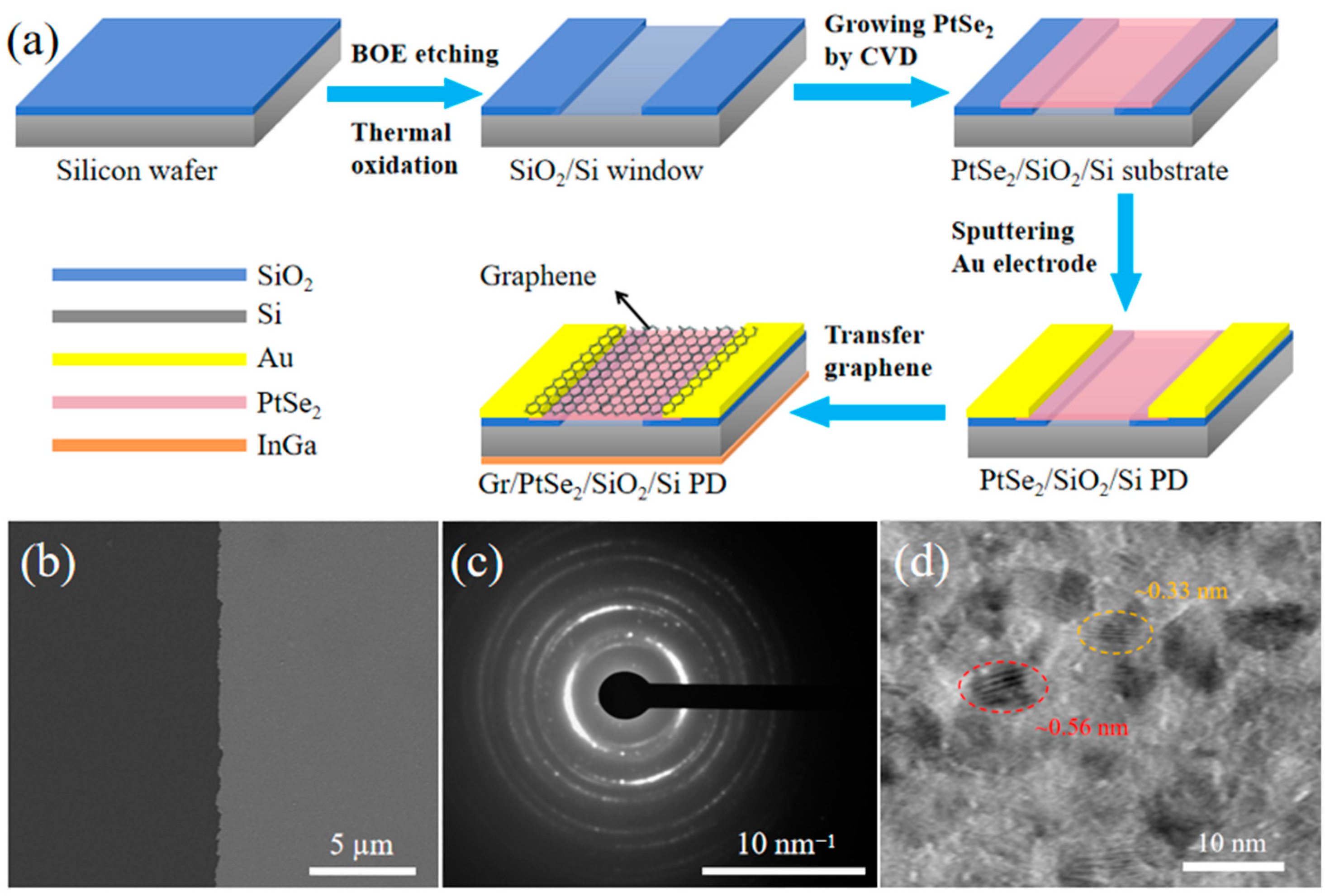
2.1. Material Synthesis and Device Fabrication

The n-type silicon substrates (resistivity: 1–10 Ω cm−1) with a 300 nm SiO2 insulating layer were used in the manufacture of heterojunction PDs. Firstly, the Si window with a size of 200 × 200 μm2 was defined by utilizing photolithography technology, and the sample was soaked in a buffered oxide etchant (HF:NH4F = 1:6) for about 3 min to remove the redundant SiO2 insulating layer. Then, the substrate was placed on a heating plate at 105 °C for 90 s to form a dense SiO2 passivation layer with a thickness of about 3.5 nm on the surface of the silicon window. Similarly, the growth region of PtSe2 material on a pre-prepared Si substrate was defined by ultraviolet photolithography technology. A Pt layer with a thickness of about 7 nm was deposited by a magnetron sputtering method (sputtering at a power of 20 W for about 60 s). Next, 900 mg selenium powder (99.99%) and the prepared Pt/ultra-thin SiO2/Si sample were placed in the upstream and downstream regions of the tube furnace, respectively. After 10 min, the temperature of the two heating regions reached 230 °C and 400 °C, respectively. During the process of thermal-assisted selenization, a vacuum pump was used to maintain the low-pressure environment in the quartz tube, and the Ar/H2 mixed gas (90/10 sccm) was continuously introduced as the carrier gas. After reacting for 90 min, the deposited Pt layer was completely selenized into the PtSe2 material. The PtSe2/ultra-thin SiO2/Si substrate was not taken out until the temperature was cooled to room temperature. Next, a Cr/Au electrode (5/50 nm) was deposited on the outer edge of the PtSe2 film by magnetron sputtering and lift-off methods. By using standard wet transfer technology (i.e., using PMMA as the supporting layer of graphene and etching the copper foil substrate with ammonium persulfate aqueous solution), graphene synthesized via the CVD method was transferred to the surface of PtSe2/ultra-thin SiO2/Si structure. Next, the redundant graphene material was removed by photolithography and an oxygen plasma etching process, thus realizing the delicate contact between the graphene layer and the device window. Finally, In-Ga alloy was coated on the back of the Si wafer to act as the bottom electrode.

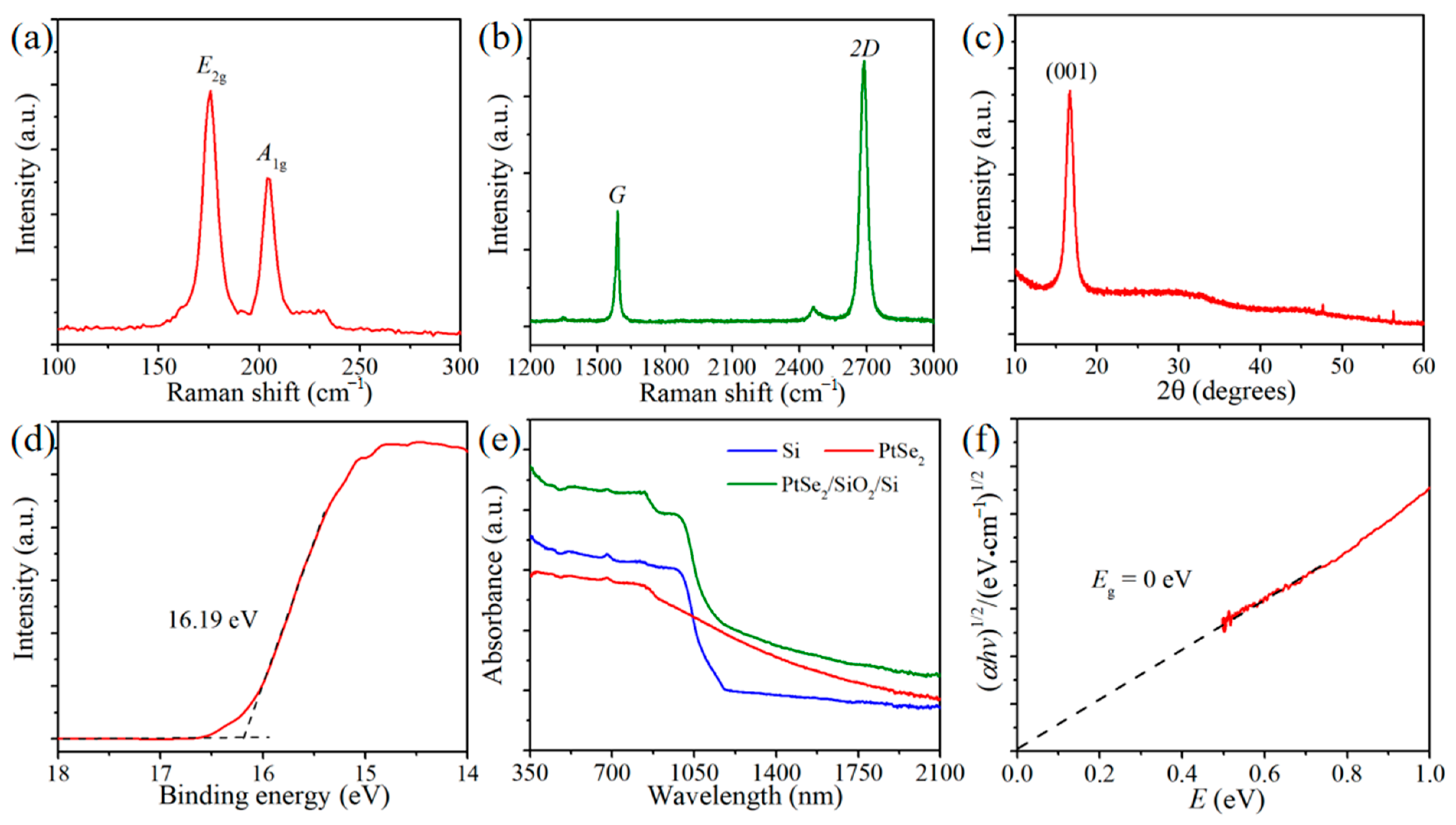
2.2. Characterization

The lattice structure of the PtSe2 film was analyzed by X-ray diffraction (XRD, Bruker, Berlin, Germany) and selected area electron diffraction (SAED, JEM 2100F, Amagasaki, Japan). Atomic force microscopy (AFM, Bruker Dimension ICON, Berlin, Germany) was performed to measure the thickness of the PtSe2 film. The thickness of the SiO2 passivation layer was evaluated by an ellipsometer (Uvisel, Horiba, Japan). The microstructure and morphology of the as-grown PtSe2 film were observed by scanning electron microscopy (SEM, Hitachi S4800, Tokyo, Japan) and transmission electron microscopy (TEM, JEM 2100F, Kitakyushu, Japan). Raman spectra of PtSe2 and graphene materials were obtained by using a 532 nm laser as excitation light on a Raman spectrometer (Horiba HR EVO, Kyoto, Japan). Ultraviolet photoelectron spectroscopy (UPS, Shimadzu Axis Supra, Manchester, UK) was employed to measure the secondary-electron cut-off region of PtSe2 film. The absorption spectra of PtSe2, Si, and PtSe2/ultra-thin SiO2/Si heterojunction were characterized by a UV–Vis–NIR spectrometer (Hitachi U-4100, Tokyo, Japan). The surface structure and morphology of the devices were observed using an optical microscope (Nikon Optiphot 200, Tokyo, Japan). The metal layers were deposited via a magnetron sputtering system (Discovery-635, New York, NY, USA). The photoelectric test platform for our heterojunction devices was composed of 375 nm, 532 nm, 808 nm, 940 nm, and 1550 nm lasers and a semiconductor parameter analyzer (FS480, Suzhou, China). In order to record the time-dependent photoresponse, the laser source was modulated by a signal generator (RIGOL DG5100, Suzhou, China) to output periodic optical signals.

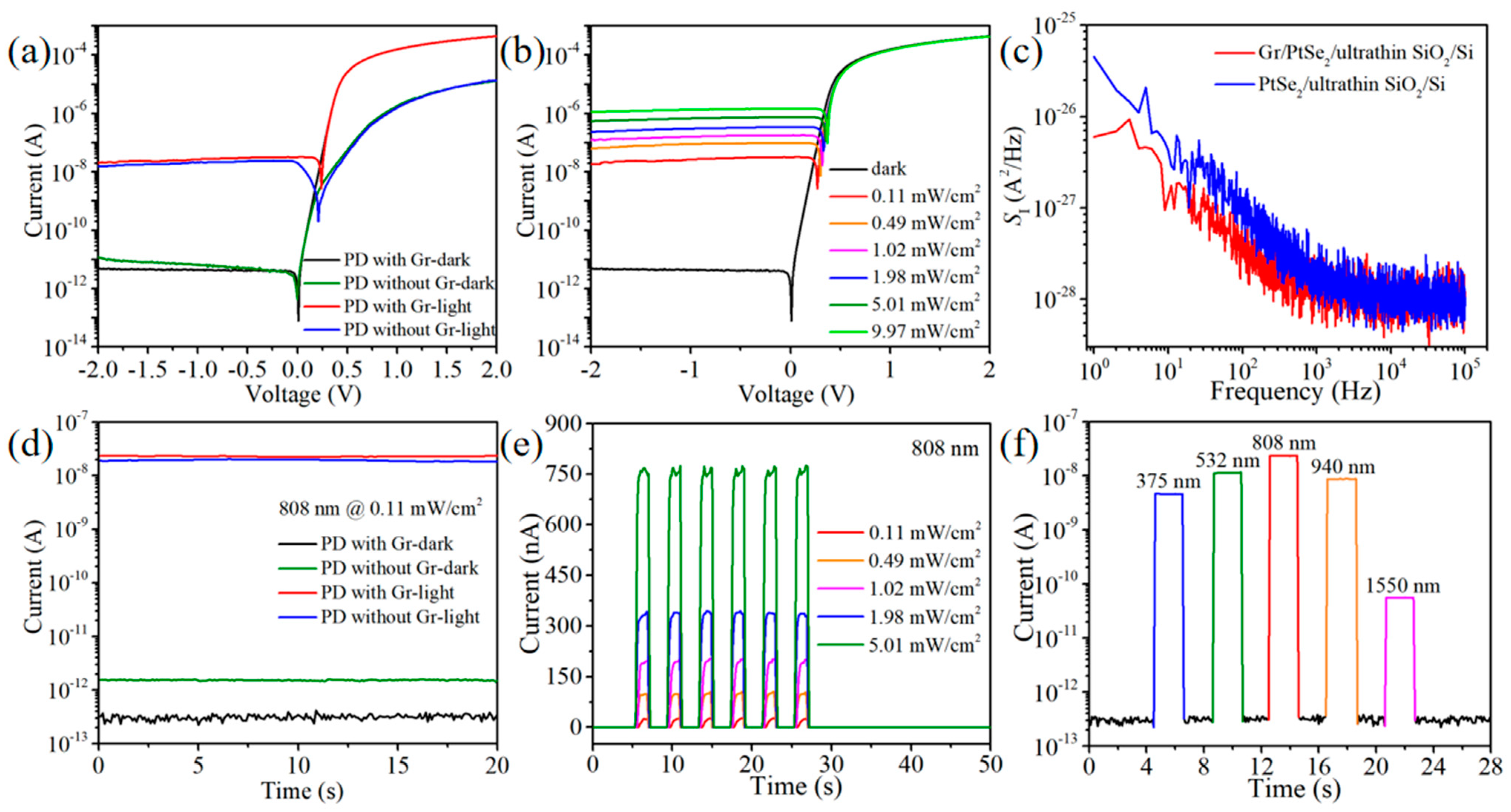
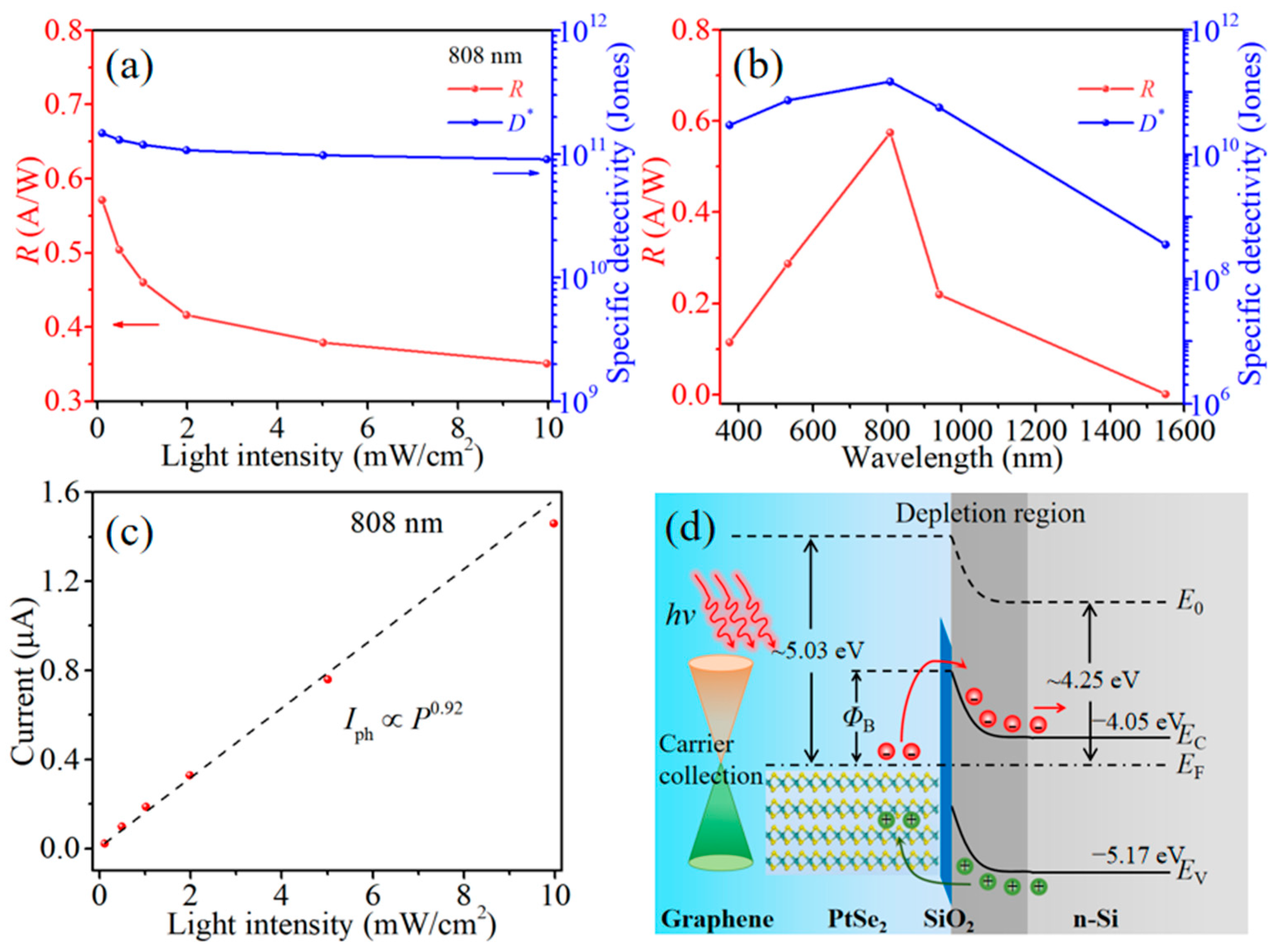
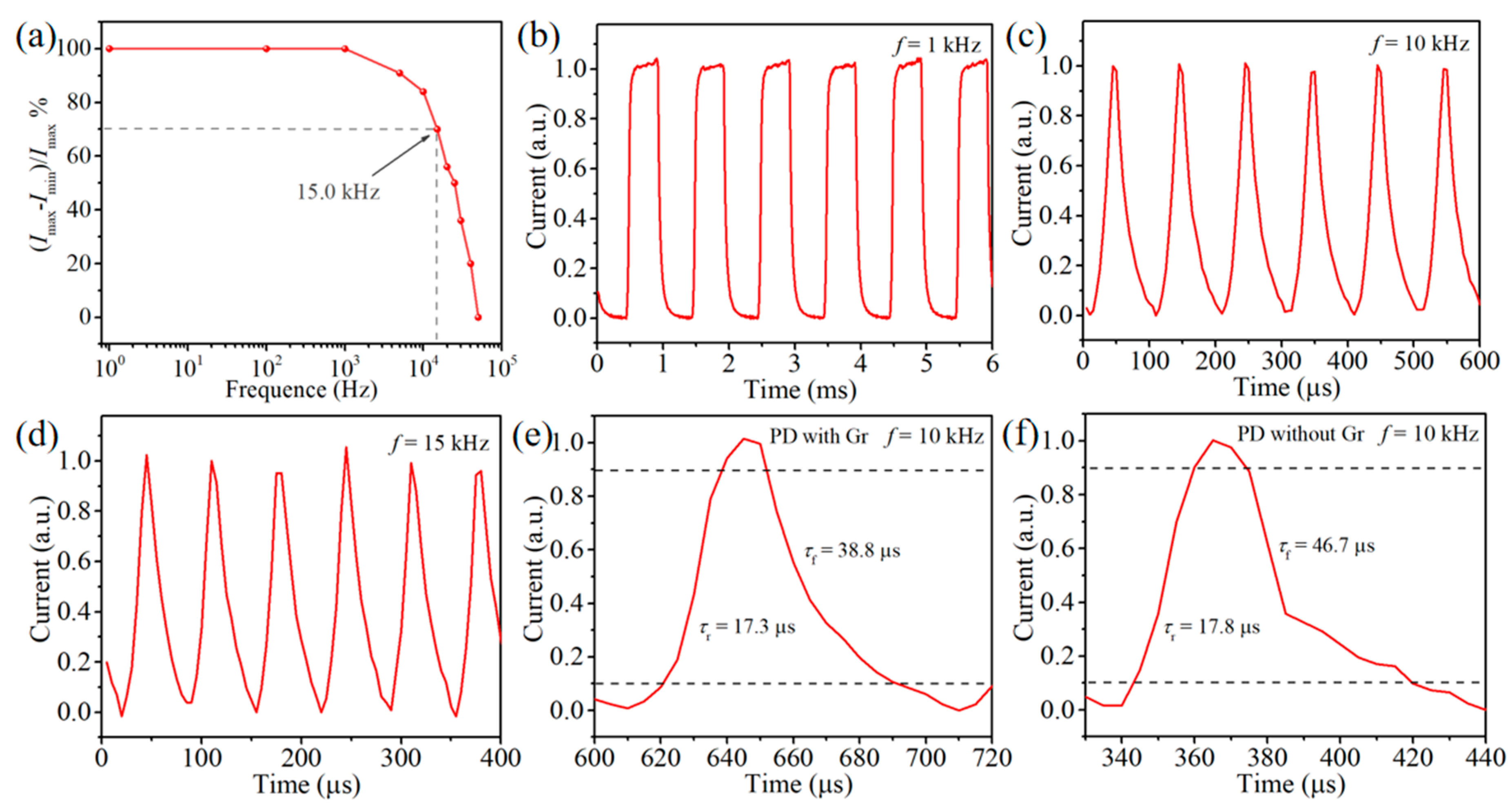
3. Results and Discussion

The schematic diagram of the preparation of PtSe2/ultra-thin SiO2/Si PDs with and without a graphene top electrode is exhibited in Figure 1a. Briefly, the Si substrate with about 300 nm of an insulating layer was etched by buffer oxide etchant and then thermally oxidized, thus exposing the n-type Si windows with an ultra-thin SiO2 passivation layer. In Figure S1, the refractive index (n) and extinction coefficient (k) values of the SiO2 film measured by ellipsometer demonstrate that a high-quality SiO2 passivation layer was formed on the bare Si windows [26], and its fitting thickness is about 3.5 nm. A dense passivation layer is usually beneficial to reduce defects at the heterojunction interface [27]. Then, the PtSe2 material was synthesized on the Si windows with the SiO2 passivation layer by a thermal-assisted selenization method. The Cr/Au electrode was deposited on the outer edge of the PtSe2 film by magnetron sputtering, obtaining the PtSe2/ultra-thin SiO2/Si heterojunction PD. Finally, graphene material was transferred to the top of the heterojunction to promote carrier collection. As seen from the SEM image in Figure 1b, the PtSe2 film synthesized on the Si substrate is continuous and quite uniform. Moreover, a number of diffraction rings with different spacing are observed by selected area electron diffraction (SAED) technology, which suggests that the PtSe2 film is a polycrystalline structure (Figure 1c). As shown in Figure 1d, the high-resolution TEM image of PtSe2 material shows lattice stripes with different orientations and spacing (such as ~0.56 nm and ~0.33 nm, corresponding to the (001) and (100) crystal planes of PtSe2, respectively), which further reveals that the polycrystalline film is composed of different PtSe2 domains. The grain boundaries between adjacent PtSe2 domains have a noticeable influence on carrier transport [28]. Therefore, it is of great significance to exploit the graphene top contact to collect photo-generated carriers in a vertical direction and make the carrier travel in the graphene plane toward the Au electrode.
Similar to other 2D TMDs, PtSe2 has a typical sandwich-like molecular structure [29]. The strong Raman peaks of our PtSe2 film at about 176 cm−1 and 207 cm−1 correspond to its Eg in-plane and A1g out-of-plane vibration modes, respectively (Figure 2a) [30]. The intensity ratio of the 2D peak at ~2691 cm−1 to that of the G peak at ~1590 cm−1 of the Raman spectrum of the graphene layer is about 2.34 (Figure 2b), suggesting its monolayer nature [31]. The negligible D peak at about 1349 cm−1 further indicates that the graphene is of high quality with low defect density [32]. In Figure S2, the Raman spectrum of the graphene/PtSe2 heterostructure contains the characteristic peaks of PtSe2 and graphene materials, which indicates that the graphene/PtSe2 interface prepared by transferring graphene to the surface of the PtSe2 film is of good quality. Furthermore, the sheet resistance of graphene film is measured to be about 450 Ω sq−1, which is smaller than that of PtSe2 film (~1030 Ω sq−1), implying that the use of graphene as the top contact is beneficial to the carrier transport. As shown in Figure 2c, XRD was utilized to further analyze the crystal structure of the material. The obvious peak at 2θ = 16.8° is assigned to the dominant (001) crystal plane of PtSe2 [33]. Based on the EDS mapping in Figure S3, the uniform and consistent distribution of Pt and Se elements implies that the metal precursor had been completely transformed into PtSe2 compound by the CVD process. As shown in Figure S4, the thickness of the PtSe2 film analyzed by atomic force microscopy (AFM) is about 28 nm. According to the secondary-electron cut-off region in Figure 2d, the Fermi energy level (EF) of the PtSe2 film can be calculated by the following formula [34]: EF = Ecutoff = 21.22 eV − 16.19 eV = 5.03 eV. The UV–Vis–NIR absorption spectra of Si, PtSe2, and the PtSe2/ultra-thin SiO2/Si heterojunction are displayed in Figure 2e. Due to the inherent band gap of about 1.12 eV, the effective absorption spectrum range of Si is limited to 1100 nm [35]. It can be found that the introduction of the PtSe2 film enhances the light absorption ability of heterojunction while expanding the detection range of Si beyond 1100 nm. As shown in Figure 2f, the fitting Tauc plot reveals that the band gap of our PtSe2 film is about 0 eV, which is consistent with related reports [36].
Figure 3a exhibits the I-V curves of the PtSe2/ultra-thin SiO2/Si heterostructures with and without a graphene top contact. The SiO2 passivation layer can suppress the recombination current at the interface of the heterojunction and has a minuscule influence on the conduction current due to the carrier tunneling effect [37,38]. Therefore, the dark state current of the PtSe2/ultra-thin SiO2/Si device is only 16.1 pA at Vbias = −2 V, while its forward current at Vbias = 2 V is as high as 12.9 μA. The graphene top contact with high conductivity can facilitate the transport of carriers once collected at the graphene/PtSe2 interface, thus reducing the recombination behavior at the lateral PtSe2 grain boundary and improving the collection efficiency of carriers. Therefore, the reverse current of the Gr/PtSe2/ultra-thin SiO2/Si device is further reduced to 4.62 pA, and its forward current is increased to 437.3 μA, leading to a large rectification ratio of 9.46 × 10⁷ at Vbias = ±2 V. Under the 808 nm illumination (0.11 mW/cm2), the PtSe2/ultra-thin SiO2/Si device achieves a short-circuit current (ISC) of 0.21 nA and an open-circuit voltage (VOC) of 0.20 V. In contrast, these values of the PD with graphene contact are improved to 2.69 nA and 0.24 V, respectively. The remarkable photovoltaic characteristics demonstrate that our devices can be used as self-driven PDs to meet the demand for low power consumption [39,40]. In order to further analyze the photovoltaic effect, I-V curves of Gr/PtSe2/ultra-thin SiO2/Si device under different light intensities are shown in Figure 3b. With the enhancement of light intensity, the photocurrent of the PD is also increased due to more photo-generated carriers being generated in the heterostructure and then separated by a strong built-in electric field. In Figure 3e, the device shows a time-dependent photocurrent with good periodicity and repeatability by intermittently turning the laser on and off. Furthermore, the device maintains a large Ilight/Idark value for weak light signals with different wavelengths from 375 nm to 1550 nm (Figure 3f), which demonstrates that our PD can realize broadband photoresponse with zero bias.
As two important figures of merit for evaluating the performance of PDs, responsivity (R) represents the photoelectric conversion efficiency of the device, while specific detectivity (D*) reflects the detection ability of PD for weak light signals [41]. The R and D* values of the PtSe2/ultra-thin SiO2/Si heterojunction with and without graphene contact can be calculated as follows [42,43]:
R = I ph P in = I light I dark P S
D * = ( S Δ f ) 1 / 2 N E P = ( S Δ f ) 1 / 2 i N R
where Ilight, Idark, P, S, and Δf are the photocurrent, dark current, incident light intensity, active illuminated area, and bandwidth, respectively. The S value is the same as the device window area of 200 × 200 μm2 (Figure S5). The equivalent noise power (NEP) is equal to the ratio of noise current (iN) to responsivity (R), that is, NEP = iN/R [44]. As shown in Figure 3c, the noise current iN of the Gr/PtSe2/ultra-thin SiO2/Si PD is calculated to be 7.75 × 10⁻¹⁴ A/Hz1/2 at Δf = 1 Hz, obviously lower than that of the PtSe2/ultra-thin SiO2/Si device (2.12 × 10⁻¹³ A/Hz1/2), which demonstrates that the graphene contact layer effectively reduces the recombination current originating from the grain boundary of the polycrystalline PtSe2 film. Under the same illumination condition, the carriers in the PtSe2/ultra-thin SiO2/Si device need to cross the grain boundary to be collected by the Au electrodes, leading to inevitable carrier loss. The PD with a graphene top contact provides a vertical collection path for photo-generated carriers in the PtSe2 film. The carriers at the graphene/PtSe2 interface can transport in the graphene plane toward the Au electrode, thus suppressing the recombination behavior at the lateral PtSe2 grain boundary and forming a larger response current. According to the photocurrent extracted in Figure 3d, the responsivities of PtSe2/ultra-thin SiO2/Si PDs with and without graphene contact under 808 nm illumination are 0.572 A/W and 0.487 A/W, respectively. Further, the external quantum efficiency (EQE) of Gr/PtSe2/ultra-thin SiO2/Si device can be calculated as EQE = Rћc/qλ = 87.5%, where ћ is the Planck constant, c is the speed of light, q is the unit charge, and λ is the wavelength of the laser [45]. Figure S6 compares the current test results of another group of devices. The PD with the Gr contact layer still shows a larger photocurrent and lower dark current, which indicates that the performance of the devices has good reproducibility. Similarly, the Gr/PtSe2/ultra-thin SiO2/Si PD obtains a D* value as high as 1.50 × 10¹¹ Jones at zero bias, which is almost 3.3 times larger than that of the device without a graphene layer (4.59 × 10¹⁰ Jones). When the recombination behavior of photo-generated carriers becomes more significant, the recombination lifetime of electron–hole pairs will be shortened [46], resulting in a decrease in the photoconductive gain (G) of the device [47]. The G value is positively correlated with photoresponse performance; as a result, the R and D* values of the device will gradually decrease with the increase in light intensity (Figure 4a). To further verify the photodetection ability of the device in a wide spectral range, Figure 4b displays the relationship between the crucial performance index and the incident wavelength. For 375 nm, 532 nm, 808 nm, 940 nm, and 1550 nm lasers, the Gr/PtSe2/ultra-thin SiO2/Si PD achieves satisfying R values of 0.115 A/W, 0.288 A/W, 0.572 A/W, 0.232 A/W, and 1.39 mA/W, respectively. Therefore, the device obtains a large rejection ratio (R808nm/R1550nm) of ~411 at zero bias voltage. The corresponding specific detectivities of the self-powered device can be calculated as 2.97 × 10¹⁰ Jones, 7.42 × 10¹⁰ Jones, 1.50 × 10¹¹ Jones, 5.71 × 10¹⁰ Jones, and 3.61 × 10⁸ Jones, respectively. Furthermore, the relationship between photocurrent and light intensity can be explained by the function IphPϴ [48]. The fitted ϴ value of 0.92 is slightly lower than an ideal value of 1 (Figure 4c), suggesting that the Gr/PtSe2/ultra-thin SiO2/Si heterojunction has an efficient photo-generated carrier collection pathway and a weak charge recombination phenomenon even in the low light intensity range [49].
In order to further illustrate the working mechanism, the schematic of the energy band structure of the Gr/PtSe2/ultra-thin SiO2/Si PD is shown in Figure 4d. When n-Si is in contact with the semi-metallic PtSe2, due to the difference in Fermi energy level between the multi-layer PtSe2 film (~5.03 eV) and the n-Si substrate (~4.25 eV), free electrons will flow from n-Si to PtSe2 films until their Fermi levels reach equilibrium. At this time, the side near PtSe2 is negatively charged, while the side near the n-Si semiconductor is positively charged, generating a Schottky barrier at the interface of the PtSe2/Si heterojunction [50]. Therefore, a strong built-in electric field from the Si to PtSe2 is formed and the energy band on the Si side will bend upward, which means that our heterojunction device has self-powered photoresponse characteristics. When the wavelength of the laser is less than 1100 nm, both the PtSe2 and Si materials can effectively absorb photon energy to excite photogenerated carriers. Under the action of the built-in electric field, the photogenerated electron–hole pairs in the heterojunction are quickly separated even without a bias voltage. Then, the photogenerated electrons inject from the PtSe2 film to Si by tunneling through the ultra-thin SiO2 layer and are captured by the bottom InGa electrode, whereas the holes in Si can drift to the PtSe2 layer and be collected by the graphene layer in a vertical direction and then travel in the graphene plane toward the Au electrode, thus resulting a large photoresponse current. Notably, the existence of an ultra-thin SiO2 passivation layer can reduce the dangling bonds and defect states of the Si surface but has negligible influence on the migration of photogenerated carriers. When the wavelength of the laser is 1550 nm, the photon energy is lower than the inherent band gap of Si (~1.12 eV). Therefore, the carriers in the heterojunction are mainly generated from the PtSe2 material with zero band gap. The electrons will tunnel through the SiO2 passivation layer to the conduction band of Si, extending the photodetection range of Si-based PD to beyond 1100 nm.
Subsequently, the modulated optical signal is utilized to investigate the frequency response of our devices. Figure 5a depicts the relative balance of (ImaxImin)/Imax versus different frequencies of the Gr/PtSe2/ultra-thin SiO2/Si PD. When the modulation frequency is about 15 kHz, the (ImaxImin)/Imax value of the device drops to 70.7%. This large 3 dB cutoff frequency indicates that the PD has the potential to respond to high-frequency light signals. The normalized photocurrents of the Gr/PtSe2/ultra-thin SiO2/Si PD with frequencies of 1 kHz, 10 kHz, and 15 kHz are exhibited in Figure 5b–d, respectively. It is found that the device maintains a repeatable and stable fast response to the various pulsed lasers. As another important indicator of a photodetector, the response speed is determined by the rising time (τr) and falling time (τf). Usually, the rising time is defined as the time required for the current to rise from 10% to 90% of the saturated photocurrent, while the falling time refers to the time required to fall from 90% to 10% of the maximum photocurrent [51]. As shown in Figure 5e, by extracting from the photocurrent at 10 kHz, the rising time and falling time of Gr/PtSe2/ultra-thin SiO2/Si PD are 17.3 μs and 38.8 μs, respectively, which are faster than those of the PD without graphene contact (17.8 μs and 46.7 μs, respectively, from Figure 5f). The enhancement of response speed can be ascribed to the fact that the graphene contact with low sheet resistance provides a vertical path for the collection of carriers. Due to the carriers being extracted by the graphene layer at the graphene/PtSe2 interface and then transported in the graphene plane toward the Au electrode, the influence of lateral grain boundaries in 2D PtSe2 films on the carrier collection becomes weak. To further evaluate the practical application prospect of our devices, Figure S7a indicates that the Gr/PtSe2/ultra-thin SiO2/Si PD possesses excellent stability and synchronization for 1000 operation cycles of turning the laser on/off. The photoresponse characteristics of the device before and after one month’s storage in ambient conditions to a pulsed signal with the same light intensity are almost identical (Figure S7b). These results demonstrate that our PD has good long-term stability and durability and can be operated reliably in atmospheric environments.
Near-infrared light possesses substantial application potential in the fields of medical treatment, agriculture, and industrial detection [52]. In order to verify the acquisition ability of Gr/PtSe2/ultra-thin SiO2/Si PDs for high-resolution image information, we have built a measurement platform for near-infrared imaging applications (Figure 6a). The optical signal with adjustable power density is generated by an 808 nm laser source. The metal mask with a hollow letter of “ZJU” is placed between the camera lens and the PD line array. A 2D rotary table is employed to control the movement of the metal mask in the horizontal and vertical directions. As shown in the photograph of real 1 × 16 pixel units in Figure S8, the linear devices array is integrated on a customized printed circuit board (PCB) to facilitate the connection with the signal collection equipment. When the laser passes through the exposed/blocked area of the mask, the control computer obtains the corresponding photocurrent/dark-current signals of the linear PD unit recorded by a data acquisition (DAQ) system in real time. The corresponding equivalent circuit diagram is shown in Figure 6b. Under 808 nm illumination, the current mapping image of the PD line array suggests that the 16 devices have good uniformity and stability (Figure 6c). Compared with the traditional infrared sensing equipment based on InSb, HgCdTe, and quantum dots/wells, our heterojunction device array shows satisfactory near-infrared imaging capability at room temperature, which proves that the Gr/PtSe2/ultra-thin SiO2/Si PD can meet the application requirements of low cost, miniaturization, and high integration [53,54,55]. We further compare the photodetection performance of our devices with other heterojunction PDs based on 2D materials (Table 1). Obviously, the responsivity of the Gr/PtSe2/ultra-thin SiO2/Si PD under near-infrared illumination is larger than that of most other heterojunction devices even at zero bias, and it shows a fast response speed comparable to these PDs. The excellent photodetection performance of the Gr/PtSe2/ultra-thin SiO2/Si device can be ascribed to the following factors: (i) The ultra-thin SiO2 passivation layer reduces the number of defects and dangling bonds on the surface of Si, thus effectively reducing the dark-state recombination current of the heterojunction. (ii) The vertically stacked heterostructure provides a strong built-in electric field in the normal direction, allowing photo-generated carriers to be rapidly separated and collected by the two-terminal electrodes, consequently obtaining a fast response time. (iii) The PtSe2 material with a narrow band gap enhances the light absorption properties of the Si substrate and expands its spectral response range. In addition, the PtSe2 layer with a unique type II Dirac cone has been proven to be beneficial to the separation and transport of carriers in the vertical direction [21,22]. (iv) The introduction of a graphene top contact with low sheet resistance improves the collection efficiency of photogenerated carriers. Due to the carriers being extracted by the graphene layer at the graphene/PtSe2 interface and then transported in the graphene plane toward the Au electrode, the carrier recombination behavior at the lateral grain boundaries of polycrystalline PtSe2 films is inhibited. Therefore, the photoresponse current of the Gr/PtSe2/ultra-thin SiO2/Si heterojunction is obviously enhanced.

4. Conclusions

In summary, we fabricated a high-performance Gr/PtSe2/ultra-thin SiO2/Si heterojunction photodetector by cooperating with various optimization mechanisms. The ultra-thin SiO2 passivation layer effectively reduces the defects and dangling bonds at the Si surface. Further, the photogenerated carriers can be rapidly extracted by the graphene top contact in a vertical direction and then transported in the graphene plane toward the Au electrode, thus inhibiting the recombination behavior of charges at the lateral grain boundaries of PtSe2 films. The self-powered device has excellent and stable photoresponse capability in a wide spectral range. Under 808 nm illumination, the Gr/PtSe2/ultra-thin SiO2/Si PD obtains an optimal responsivity of 0.572 A/W, a high specific detectivity of 1.50 × 10¹¹ Jones, and a fast response time of 17.3/38.8 μs. In addition, the PDs line array exhibits good uniformity and near-infrared imaging ability at room temperature. Our research will provide new impetus for the rise of high-performance heterostructure photodetectors based on 2D materials.

Supplementary Materials

The following supporting information can be downloaded at: https://www.mdpi.com/article/10.3390/nano15070519/s1, Figure S1: n, k values of the SiO2 passivation layer; Figure S2: Raman spectrum of Gr/PtSe2 heterostructure; Figure S3: TEM image and EDS mapping of PtSe2 film; Figure S4: AFM image of PtSe2; Figure S5: OM images of the PDs; Figure S6: The current of another batch of devices.; Figure S7: Stability and reliability testing of our device; Figure S8: Photograph of the imaging test platform.

Author Contributions

Conceptualization, Q.-H.Z. and M.-S.X.; methodology, Q.-H.Z. and M.-S.X.; investigation, Q.-H.Z.; resources, M.-S.X.; data curation, Q.-H.Z. and J.C.; writing—original draft, Q.-H.Z. and S.-Y.W.; writing—review and editing, J.-B.S., Y.-J.S., D.K. and M.-S.X.; visualization, Q.-H.Z.; supervision, M.-S.X. All authors have read and agreed to the published version of the manuscript.

Funding

This work was supported by the National Natural Science Foundation of China (62090030/62090031, 62274145) and the National Key R&D Program of China (2021YFA1200502). The authors would like to acknowledge the fabrication support from ZJU Micro-Nano Fabrication Center and thank Bi Chao from the Core Facilities at the School of Medicine in Zhejiang University for Raman measurement.

Data Availability Statement

Data are contained within the article.

Conflicts of Interest

The authors declare no conflicts of interest.

References

  1. Pospischil, A.; Humer, M.; Furchi, M.M.; Bachmann, D.; Guider, R.; Fromherz, T.; Mueller, T. CMOS-compatible graphene photodetector covering all optical communication bands. Nat. Photonics 2013, 7, 892–896. [Google Scholar]
  2. Liu, S.; Ding, Y.; Wang, X.; Li, Y.; Chen, J.; Zhao, Z.; Zhu, Z. High Gain Derived from Facile Carrier Dynamics Manipulation for Sensitive X-ray Detection and Imaging. Adv. Electron. Mater. 2024, 10, 2300555. [Google Scholar] [CrossRef]
  3. Wang, H.; Li, Z.; Li, D.; Chen, P.; Pi, L.; Zhou, X.; Zhai, T. Van der Waals integration based on two-dimensional materials for high-performance infrared photodetectors. Adv. Funct. Mater. 2021, 31, 2103106. [Google Scholar] [CrossRef]
  4. Huang, Z.; Carey, J.E.; Liu, M.; Guo, X.; Mazur, E.; Campbell, J.C. Microstructured silicon photodetector. Appl. Phys. Lett. 2006, 89, 033506. [Google Scholar]
  5. Michel, J.; Liu, J.; Kimerling, L.C. High-performance Ge-on-Si photodetectors. Nat. Photonics 2010, 4, 527–534. [Google Scholar]
  6. Zhu, Q.; Ye, P.; Tang, Y.; Zhu, X.; Cheng, Z.; Xu, J.; Xu, M. High-performance broadband photoresponse of self-powered Mg2Si/Si photodetectors. Nanotechnology 2021, 33, 115202. [Google Scholar]
  7. Geng, X.; Wang, F.; Tian, H.; Feng, Q.; Zhang, H.; Liang, R.; Shen, Y.; Ju, Z.; Gou, G.-Y.; Deng, N. Ultrafast photodetector by integrating perovskite directly on silicon wafer. ACS Nano 2020, 14, 2860–2868. [Google Scholar]
  8. Chen, J.; Ouyang, W.; Yang, W.; He, J.H.; Fang, X. Recent progress of heterojunction ultraviolet photodetectors: Materials, integrations, and applications. Adv. Funct. Mater. 2020, 30, 1909909. [Google Scholar] [CrossRef]
  9. Wang, S.; Liu, X.; Xu, M.; Liu, L.; Yang, D.; Zhou, P. Two-dimensional devices and integration towards the silicon lines. Nat. Mater. 2022, 21, 1225–1239. [Google Scholar]
  10. Liu, C.; Guo, J.; Yu, L.; Li, J.; Zhang, M.; Li, H.; Shi, Y.; Dai, D. Silicon/2D-material photodetectors: From near-infrared to mid-infrared. Light Sci. Appl. 2021, 10, 123. [Google Scholar]
  11. Xu, M.; Liang, T.; Shi, M.; Chen, H. Graphene-like two-dimensional materials. Chem. Rev. 2013, 113, 3766–3798. [Google Scholar] [PubMed]
  12. Li, X.; Zhu, M.; Du, M.; Lv, Z.; Zhang, L.; Li, Y.; Yang, Y.; Yang, T.; Li, X.; Wang, K. High detectivity graphene-silicon heterojunction photodetector. Small 2016, 12, 595–601. [Google Scholar] [PubMed]
  13. Huang, L.; Dong, B.; Guo, X.; Chang, Y.; Chen, N.; Huang, X.; Liao, W.; Zhu, C.; Wang, H.; Lee, C. Waveguide-integrated black phosphorus photodetector for mid-infrared applications. ACS Nano 2018, 13, 913–921. [Google Scholar]
  14. Han, R.; Feng, S.; Sun, D.-M.; Cheng, H.-M. Properties and photodetector applications of two-dimensional black arsenic phosphorus and black phosphorus. Sci. China Inform. Sci. 2021, 64, 140402. [Google Scholar]
  15. Lan, C.; Li, C.; Ho, J.C.; Liu, Y. 2D WS2: From vapor phase synthesis to device applications. Adv. Electron. Mater. 2021, 7, 2000688. [Google Scholar]
  16. Xue, H.; Dai, Y.; Kim, W.; Wang, Y.; Bai, X.; Qi, M.; Halonen, K.; Lipsanen, H.; Sun, Z. High photoresponsivity and broadband photodetection with a band-engineered WSe2/SnSe2 heterostructure. Nanoscale 2019, 11, 3240–3247. [Google Scholar]
  17. Gant, P.; Huang, P.; de Lara, D.P.; Guo, D.; Frisenda, R.; Castellanos-Gomez, A. A strain tunable single-layer MoS2 photodetector. Mater. Today 2019, 27, 8–13. [Google Scholar]
  18. Yang, Y.; Li, J.; Choi, S.; Jeon, S.; Cho, J.H.; Lee, B.H.; Lee, S. High-responsivity PtSe2 photodetector enhanced by photogating effect. Appl. Phys. Lett. 2021, 118, 013103. [Google Scholar]
  19. Wang, G.; Wang, Z.; McEvoy, N.; Fan, P.; Blau, W.J. Layered PtSe2 for sensing, photonic, and (opto-) electronic applications. Adv. Mater. 2021, 33, 2004070. [Google Scholar] [CrossRef]
  20. Cao, B.; Ye, Z.; Yang, L.; Gou, L.; Wang, Z. Recent progress in van der Waals 2D PtSe2. Nanotechnology 2021, 32, 412001. [Google Scholar]
  21. Xu, H.; Guo, C.; Zhang, J.; Guo, W.; Kuo, C.N.; Lue, C.S.; Hu, W.; Wang, L.; Chen, G.; Politano, A. PtTe2-based type-II Dirac semimetal and its van der Waals heterostructure for sensitive room temperature terahertz photodetection. Small 2019, 15, 1903362. [Google Scholar] [CrossRef] [PubMed]
  22. Wu, D.; Zhao, Z.; Lu, W.; Rogée, L.; Zeng, L.; Lin, P.; Shi, Z.; Tian, Y.; Li, X.; Tsang, Y.H. Highly sensitive solar-blind deep ultraviolet photodetector based on graphene/PtSe2/β-Ga2O3 2D/3D Schottky junction with ultrafast speed. Nano Res. 2021, 14, 1973–1979. [Google Scholar] [CrossRef]
  23. Xie, C.; Zeng, L.; Zhang, Z.; Tsang, Y.-H.; Luo, L.; Lee, J.-H. High-performance broadband heterojunction photodetectors based on multilayered PtSe2 directly grown on a Si substrate. Nanoscale 2018, 10, 15285–15293. [Google Scholar] [PubMed]
  24. Ma, M.; Chen, H.; Zhou, K.; Xie, C.; Liang, Y.; Wang, L.; Wu, C.; Yang, W.; Guo, J.; Luo, L. Multilayered PtSe2/pyramid-Si heterostructure array with light confinement effect for high-performance photodetection, image sensing and light trajectory tracking applications. J. Mater. Chem. C 2021, 9, 2823–2832. [Google Scholar]
  25. Ye, P.; Xiao, H.; Zhu, Q.; Kong, Y.; Tang, Y.; Xu, M. Si-CMOS-compatible 2D PtSe2-based self-driven photodetector with ultrahigh responsivity and specific detectivity. Sci. China Mater. 2023, 66, 193–201. [Google Scholar]
  26. Jellison Jr, G. Examination of thin SiO2 films on Si using spectroscopic polarization modulation ellipsometry. J. Appl. Phys. 1991, 69, 7627–7634. [Google Scholar]
  27. Rao, G.; Wang, X.; Wang, Y.; Wangyang, P.; Yan, C.; Chu, J.; Xue, L.; Gong, C.; Huang, J.; Xiong, J. Two-dimensional heterostructure promoted infrared photodetection devices. InfoMat 2019, 1, 272–288. [Google Scholar]
  28. Zeng, L.; Han, W.; Wu, S.-E.; Wu, D.; Lau, S.P.; Tsang, Y.H. Graphene/PtSe2/pyramid Si Van der Waals schottky junction for room-temperature broadband infrared light detection. IEEE T. Electron Dev. 2022, 69, 6212–6216. [Google Scholar]
  29. Tong, Y.; Bouaziz, M.; Oughaddou, H.; Enriquez, H.; Chaouchi, K.; Nicolas, F.; Kubsky, S.; Esaulov, V.; Bendounan, A. Phase transition and thermal stability of epitaxial PtSe2 nanolayer on Pt(111). RSC Adv. 2020, 10, 30934–30943. [Google Scholar]
  30. Yin, S.; Zhang, W.; Tan, C.; Chen, L.; Chen, J.; Li, G.; Zhang, H.; Zhang, Y.; Wang, W.; Li, L. Thermal conductivity of few-layer PtS2 and PtSe2 obtained from optothermal Raman spectroscopy. J. Phys. Chem. C 2021, 125, 16129–16135. [Google Scholar]
  31. Li, X.; Cai, W.; An, J.; Kim, S.; Nah, J.; Yang, D.; Piner, R.; Velamakanni, A.; Jung, I.; Tutuc, E. Large-area synthesis of high-quality and uniform graphene films on copper foils. Science 2009, 324, 1312–1314. [Google Scholar] [CrossRef] [PubMed]
  32. Ni, Z.; Wang, Y.; Yu, T.; Shen, Z. Raman spectroscopy and imaging of graphene. Nano Res. 2008, 1, 273–291. [Google Scholar] [CrossRef]
  33. Lin, S.; Liu, Y.; Hu, Z.; Lu, W.; Mak, C.H.; Zeng, L.; Zhao, J.; Li, Y.; Yan, F.; Tsang, Y.H. Tunable active edge sites in PtSe2 films towards hydrogen evolution reaction. Nano Energy 2017, 42, 26–33. [Google Scholar] [CrossRef]
  34. Zeng, L.H.; Lin, S.H.; Li, Z.J.; Zhang, Z.X.; Zhang, T.F.; Xie, C.; Mak, C.H.; Chai, Y.; Lau, S.P.; Luo, L.B. Fast, self-driven, air-stable, and broadband photodetector based on vertically aligned PtSe2/GaAs heterojunction. Adv. Funct. Mater. 2018, 28, 1705970. [Google Scholar] [CrossRef]
  35. Ranjan, V.; Kapoor, M.; Singh, V.A. The band gap in silicon nanocrystallites. J. Phys.-Condens. Mat. 2002, 14, 6647. [Google Scholar] [CrossRef]
  36. Wang, L.; Zhang, S.; McEvoy, N.; Sun, Y.y.; Huang, J.; Xie, Y.; Dong, N.; Zhang, X.; Kislyakov, I.M.; Nunzi, J.M. Nonlinear optical signatures of the transition from semiconductor to semimetal in PtSe2. Laser Photonics Rev. 2019, 13, 1900052. [Google Scholar] [CrossRef]
  37. Yang, M.; Luo, Z.; Gao, W.; Zhang, M.; Huang, L.; Zhao, Y.; Yao, J.; Wu, F.; Li, J.; Zheng, Z. Robust Deposition of Sub-Millimeter WSe2 Drive Ultrasensitive Gate-Tunable 2D Material Photodetectors. Adv. Opt. Mater. 2022, 10, 2200717. [Google Scholar] [CrossRef]
  38. Xu, M.; Xu, Z.; Sun, Z.; Chen, W.; Wang, L.; Liu, Y.; Wang, Y.; Du, X.; Pan, S. Surface engineering in SnO2/Si for high-performance broadband photodetectors. ACS Appl. Mater. Interfaces 2023, 15, 3664–3672. [Google Scholar] [CrossRef]
  39. Zhou, C.; Raju, S.; Li, B.; Chan, M.; Chai, Y.; Yang, C.Y. Self-driven metal–semiconductor–metal WSe2 photodetector with asymmetric contact geometries. Adv. Funct. Mater. 2018, 28, 1802954. [Google Scholar] [CrossRef]
  40. Vashishtha, P.; Abidi, I.H.; Giridhar, S.P.; Verma, A.K.; Prajapat, P.; Bhoriya, A.; Murdoch, B.J.; Tollerud, J.O.; Xu, C.; Davis, J.A. CVD-grown monolayer MoS2 and GaN thin film heterostructure for a self-powered and bidirectional photodetector with an extended active spectrum. ACS Appl. Mater. Interfaces 2024, 16, 31294–31303. [Google Scholar] [CrossRef]
  41. Liu, C.-H.; Chang, Y.-C.; Norris, T.B.; Zhong, Z. Graphene photodetectors with ultra-broadband and high responsivity at room temperature. Nat. Nanotechnol. 2014, 9, 273–278. [Google Scholar]
  42. Chen, Y.; Zhu, Q.; Zhu, X.; Sun, Y.; Cheng, Z.; Xu, J.; Xu, M. Gate-tunable high-performance broadband phototransistor array of two-dimensional PtSe2 on SOI. Nano Res. 2023, 16, 7559–7567. [Google Scholar]
  43. Xiao, H.; Liang, T.; Xu, M. Growth of Ultraflat PbI2 nanoflakes by solvent evaporation suppression for high-performance UV photodetectors. Small 2019, 15, 1901767. [Google Scholar]
  44. Crisci, T.; Moretti, L.; Casalino, M. Theoretical investigation of responsivity/NEP trade-off in NIR graphene/semiconductor schottky photodetectors operating at room temperature. Appl. Sci. 2021, 11, 3398. [Google Scholar] [CrossRef]
  45. Vashishtha, P.; Goswami, L.; Jain, S.K.; Aggarwal, N.; Gupta, G. GaN-djoser pyramidal self powered UV photodetector for optical signal detection in rugged environments. J. Alloy. Compd. 2023, 930, 167267. [Google Scholar]
  46. Chen, Z.; Cheng, Z.; Wang, J.; Wan, X.; Shu, C.; Tsang, H.K.; Ho, H.P.; Xu, J.B. High responsivity, broadband, and fast graphene/silicon photodetector in photoconductor mode. Adv. Opt. Mater. 2015, 3, 1207–1214. [Google Scholar]
  47. Vashishtha, P.; Prajapat, P.; Kumar, K.; Kumar, M.; Walia, S.; Gupta, G. Multiband spectral response inspired by ultra-high responsive thermally stable and self-powered Sb2Se3/GaN heterojunction based photodetector. Surf. Interfaces 2023, 42, 103376. [Google Scholar]
  48. Xu, L.; Qin, L.; Huang, Y.; Meng, Y.; Xu, J.; Zhao, L.; Zhou, W.; Wang, Q.; Hao, G.; Sun, J. Super high-speed self-powered photodetector based on solution-processed transparent p-type amorphous phosphorous-doped SnO film. Sci. China Mater. 2024, 67, 690–697. [Google Scholar]
  49. Won, U.Y.; Lee, B.H.; Kim, Y.R.; Kang, W.T.; Lee, I.; Kim, J.E.; Lee, Y.H.; Yu, W.J. Efficient photovoltaic effect in graphene/h-BN/silicon heterostructure self-powered photodetector. Nano Res. 2021, 14, 1967–1972. [Google Scholar]
  50. Zeng, L.; Lin, S.; Lou, Z.; Yuan, H.; Long, H.; Li, Y.; Lu, W.; Lau, S.P.; Wu, D.; Tsang, Y.H. Ultrafast and sensitive photodetector based on a PtSe2/silicon nanowire array heterojunction with a multiband spectral response from 200 to 1550 nm. NPG Asia Mater. 2018, 10, 352–362. [Google Scholar]
  51. Zhao, Y.; Li, C.; Shen, L. Recent advances on organic-inorganic hybrid perovskite photodetectors with fast response. InfoMat 2019, 1, 164–182. [Google Scholar]
  52. Lu, R.; Ge, C.W.; Zou, Y.F.; Zheng, K.; Wang, D.D.; Zhang, T.F.; Luo, L.B. A localized surface plasmon resonance and light confinement-enhanced near-infrared light photodetector. Laser Photonics Rev. 2016, 10, 595–602. [Google Scholar]
  53. Lei, W.; Antoszewski, J.; Faraone, L. Progress, challenges, and opportunities for HgCdTe infrared materials and detectors. Appl. Phys. Rev. 2015, 2, 041303. [Google Scholar]
  54. Rogalski, A. Quantum well photoconductors in infrared detector technology. J. Appl. Phys. 2003, 93, 4355–4391. [Google Scholar]
  55. Azizur-Rahman, K.; LaPierre, R. Optical design of a mid-wavelength infrared InSb nanowire photodetector. Nanotechnology 2016, 27, 315202. [Google Scholar]
  56. Yu, T.; Wang, F.; Xu, Y.; Ma, L.; Pi, X.; Yang, D. Graphene coupled with silicon quantum dots for high-performance bulk-silicon-based Schottky-junction photodetectors. Adv. Mater. 2016, 28, 4912–4919. [Google Scholar] [CrossRef]
  57. An, X.; Liu, F.; Jung, Y.J.; Kar, S. Tunable graphene–silicon heterojunctions for ultrasensitive photodetection. Nano Lett. 2013, 13, 909–916. [Google Scholar]
  58. Zeng, L.; Wu, D.; Jie, J.; Ren, X.; Hu, X.; Lau, S.P.; Chai, Y.; Tsang, Y.H. Van der Waals epitaxial growth of mosaic-like 2D platinum ditelluride layers for room-temperature mid-infrared photodetection up to 10.6 µm. Adv. Mater. 2020, 32, 2004412. [Google Scholar]
  59. Wu, D.; Guo, J.; Du, J.; Xia, C.; Zeng, L.; Tian, Y.; Shi, Z.; Tian, Y.; Li, X.J.; Tsang, Y.H. Highly polarization-sensitive, broadband, self-powered photodetector based on graphene/PdSe2/germanium heterojunction. ACS Nano 2019, 13, 9907–9917. [Google Scholar]
  60. Zhu, Q.; Wei, S.; Sun, J.; Sun, Y.; Xu, M. Two-dimensional PtSe2 thin-film coupled with a graphene/Si Schottky-junction for a high performance photodetector. Nanoscale 2024, 16, 19865–19872. [Google Scholar]
  61. Wu, E.; Wu, D.; Jia, C.; Wang, Y.; Yuan, H.; Zeng, L.; Xu, T.; Shi, Z.; Tian, Y.; Li, X. In situ fabrication of 2D WS2/Si type-II heterojunction for self-powered broadband photodetector with response up to mid-infrared. ACS Photonics 2019, 6, 565–572. [Google Scholar]
  62. Hao, L.; Wang, Z.; Xu, H.; Yan, K.; Dong, S.; Liu, H.; Du, Y.; Wu, Y.; Liu, Y.; Dong, M. 2D SnSe/Si heterojunction for self-driven broadband photodetectors. 2D Mater. 2019, 6, 034004. [Google Scholar] [CrossRef]
  63. Jia, C.; Wu, D.; Wu, E.; Guo, J.; Zhao, Z.; Shi, Z.; Xu, T.; Huang, X.; Tian, Y.; Li, X. A self-powered high-performance photodetector based on a MoS2/GaAs heterojunction with high polarization sensitivity. J. Mater. Chem. C 2019, 7, 3817–3821. [Google Scholar]
Figure 1. (a) Schematic diagram of the preparation of PtSe2/ultra-thin SiO2/Si PDs with and without graphene top electrode. (b) SEM image of PtSe2 film (right half area) grown on the silicon substrate. (c) SAED pattern of PtSe2 film. (d) TEM image of PtSe2 material with high-resolution magnification.
Nanomaterials 15 00519 g001
Figure 2. Raman spectra of (a) PtSe2 film and (b) graphene. (c) XRD pattern and (d) secondary-electron cut-off region of the PtSe2 thin film on the silicon substrate. (e) UV–Vis–NIR absorption spectra of Si, PtSe2, and PtSe2/ultra-thin SiO2/Si heterojunction. (f) Tauc plot of the 2D PtSe2 film.
Nanomaterials 15 00519 g002
Figure 3. (a) I-V curves of the PtSe2/ultra-thin SiO2/Si heterojunction PDs with and without a graphene top contact in the dark and under 808 nm illumination. The light intensity is 0.11 mW/cm2. (b) I-V characteristics of Gr/PtSe2/ultra-thin SiO2/Si PD measured in the dark and 808 nm illumination with different light intensities. (c) The noise density spectra of our devices as a function of frequency. (d) Currents of PtSe2/ultra-thin SiO2/Si and Gr/PtSe2/ultra-thin SiO2/Si PDs in the dark and under 808 nm laser illumination at a voltage of 0 V. (e) Corresponding time-dependent photovoltaic response of Gr/PtSe2/ultra-thin SiO2/Si PD with different 808 nm light intensities at Vbias = 0 V. (f) Corresponding photovoltaic response of Gr/PtSe2/ultra-thin SiO2/Si PD under different incident light wavelengths at Vbias = 0 V. All the light intensities are about 0.11 mW/cm2.
Nanomaterials 15 00519 g003
Figure 4. R and D* values of Gr/PtSe2/ultra-thin SiO2/Si PD as a function of (a) light intensity under 808 nm illumination and (b) incident laser wavelength at Vbias = 0 V. (c) Dependence of photocurrent on the light intensity at 808 nm illumination. (d) Energy band diagram of Gr/PtSe2/ultra-thin SiO2/Si device under laser irradiation.
Nanomaterials 15 00519 g004
Figure 5. (a) Relative balance of (ImaxImin)/Imax versus different frequencies of the Gr/PtSe2/ultra-thin SiO2/Si device. Normalized photocurrents of Gr/PtSe2/ultra-thin SiO2/Si PD with different light frequencies of (b) 1, (c) 10, and (d) 15 kHz. Response speed of PtSe2/ultra-thin SiO2/Si PD (e) with and (f) without graphene material extracted at 10 kHz for 808 nm illumination.
Nanomaterials 15 00519 g005
Figure 6. (a) Schematic of the experimental platform for near-infrared imaging with a Gr/PtSe2/ultra-thin SiO2/Si line array. (b) Equivalent circuit diagram of linear PD array used in imaging applications. (c) The photocurrent mapping image of the PDs array for the “ZJU” mask under 808 nm illumination.
Nanomaterials 15 00519 g006
Table 1. Properties comparison of our PtSe2/ultra-thin SiO2/Si PDs with and without a graphene electrode to other relevant van der Waals PDs.
Devicesλ @ VbiasR (A/W)τr/τfSpectral RangeRef.
Si-QD/Gr/Si877 nm @ −1 V0.495/300–1000 nm[56]
Gr/Si875 nm @ −2 V0.435~1.7 ms400–900 nm[57]
PtSe2/Si808 nm @ 0 V0.5255.3/171 μs200–1550 nm[23]
Gr/PtSe2/pyramid Si980 nm @ 0 V0.5288.5/10.2 μs980–10,600 nm[28]
Gr/PtTe2/Si808 nm @ 0 V0.4282.4/32.0 μs808–10,600 nm[58]
Gr/PdSe2/Ge980 nm @ 0 V0.6916.4/92.5 μs265–3040 nm[59]
PtSe2/Gr/Si808 nm @ −1 V0.8143.6/51.2 μs375–940 nm[60]
WS2/Si980 nm @ 0 V0.22416/29 μs200–3043 nm[61]
SnSe/Si850 nm @ 0 V0.5671.6/47.7 μs300–1100 nm[62]
WS2/GaAs808 nm @ 0 V0.52721.8/49.6 μs 200–1550 nm[63]
PtSe2/ultra-thin SiO2/Si808 nm @ 0 V0.48717.8/46.7 μs/This work
Gr/PtSe2/ultra-thin SiO2/Si808 nm @ 0 V0.57217.3/38.8 μs375–1550 nmThis work
Disclaimer/Publisher’s Note: The statements, opinions and data contained in all publications are solely those of the individual author(s) and contributor(s) and not of MDPI and/or the editor(s). MDPI and/or the editor(s) disclaim responsibility for any injury to people or property resulting from any ideas, methods, instructions or products referred to in the content.

