Article

Synthesis, Structure, and Optoelectronic Properties of a Hybrid Organic–Inorganic Perovskite with a Monoethanolammonium Cation MAxMEA1−xPbI3

1
Laboratory of Nonequilibrium Processes in Semiconductors, Ioffe Institute, 26 Politekhnicheskaya, Saint Petersburg 194021, Russia
2
Department of Micro and Nanoelectronics, Belarusian State University of Informatics and Radioelectronics, 220013 Minsk, Belarus
3
Department of Micro and Nanoelectronics, Saint Petersburg Electrotechnical University “LETI”, Saint Petersburg 197022, Russia
4
Solid State Electronics Department, Saint Petersburg State University, Saint Petersburg 199034, Russia
*
Authors to whom correspondence should be addressed.
Nanomaterials 2025, 15(7), 494; https://doi.org/10.3390/nano15070494
Submission received: 20 February 2025 / Revised: 21 March 2025 / Accepted: 24 March 2025 / Published: 26 March 2025
(This article belongs to the Section Nanoelectronics, Nanosensors and Devices)

Abstract

Hybrid organic–inorganic perovskites have emerged as promising materials for next-generation optoelectronic devices owing to their tunable properties and low-cost fabrication. We report the synthesis of 3D hybrid perovskites with monoethanolammonium cations. Specifically, we investigated the optoelectronic properties and morphological characteristics of polycrystalline films of hybrid perovskites MAxMEA1−xPbI3, which contain methylammonium (MA) and monoethanolammonium (MEA) cations. MAxMEA1−xPbI3 crystallizes in a tetragonal perovskite structure. The substitution of methylammonium cations with monoethanolammonium ions led to an increase in the lattice parameters and the bandgap energy. Energy level diagrams of the synthesized samples were also constructed. The bandgap of MA0.5MEA0.5PbI3 makes it a promising material for use in tandem solar cells. These polycrystalline films, namely MA0.5MEA0.5PbI3 and MA0.25MEA0.75PbI3 were fabricated using a one-step spin-coating method without an antisolvent. These films exhibit a uniform surface morphology under the specified deposition parameters. Within the scope of this study, no evidence of dendritic structures or pinhole-type defects were observed. All synthesized samples demonstrated photocurrent generation under visible light illumination. Moreover, using monoethanolammonium cations reduced the hysteresis of the I–V characteristics, indicating improved device stability.

1. Introduction

The performance of hybrid organic–inorganic perovskite solar cells has led to a recent surge in interest in perovskite materials [1,2]. Inorganic and fully organic metal-free halogen perovskites have been the subject of more research due to the growing interest in hybrid perovskite materials [3,4,5,6,7,8]. Bulk (3D) hybrid perovskite materials (polycrystalline layers or single crystals), two-dimensional (2D), one-dimensional (1D), and zero-dimensional (0D) perovskite materials are thought to be very appealing for optoelectronic applications and have a wide range of uses [9,10,11,12,13,14,15,16,17].
A bandgap that is ideal for absorbing sunlight, a direct bandgap structure, a high absorption coefficient, high mobility, and a long average free path of the charge carriers are some of the special qualities that make hybrid perovskite solar cells effective [18,19]. By altering the composition of the hybrid perovskites, the bandgap can be adjusted, thereby controlling the absorption spectrum of the tandem solar cell. This is crucial for the growth of the silicon solar cell market, which may employ hybrid perovskites with a wider bandgap [20,21]. It is notable that a polycrystalline hybrid perovskite film can be produced from solution crystallized at low temperatures (about 100 °C). Perovskite films can be made using a variety of techniques, including spin coating, screen printing, inkjet, spraying, and doctor blades [2,22,23]. These application techniques have the advantage of being compatible with silicon solar cells and having low mass production costs. Hybrid perovskites can be utilized to make X-ray detectors, optically excited memristors, and light-emitting devices [24,25,26,27,28].
Currently, a wide range of compositions of polycrystalline films based on APbX3 has been proposed for the creation of photovoltaic structures, usually with a variation in the proportions of formamidinium (FA+, CH(NH2)2+) and methylammonium (MA+, CH3NH3+) cations and I, Br, and Cl anions, as well as the introduction of inorganic cations or partial replacement of lead [29,30,31,32]. The search for complex compositions of hybrid perovskites aims to improve stability while ensuring optimal values of the bandgap and solar cell efficiency [2]. Molecular passivation and the formation of films from 3D/2D perovskites can be used to reduce the degradation phenomena of perovskite photovoltaic structures [33,34,35,36]. For this purpose, as a rule, long-chain amines are used, which interact with uncoordinated Pb ions with terminal -NH2 groups and passivate defects at the periphery of grains. Also, some short-chain amines can act as organic linkers between inorganic octahedral frameworks in quasi-2D perovskites [34]. Nowadays, 2D perovskite organic–inorganic perovskite materials are divided into three phase types: Ruddlesden–Popper (RP) phase, Dion–Jacobson (DJ) phase, and alternating cations in interlayer space (ACI) phases and corresponding quasi-2D phases (layered perovskites) with general formulas A′2An−1BnX3n+1 (for RP), A′An−1BnX3n+1 (for DJ) и A′AnBnX3n+1 (for ACI), where n is the number of octahedral layers, A′ is spacer cations [9,37]. The chemical composition of 3D perovskites is typically designed so that the Goldschmidt tolerance factor falls within the range of 0.8 to 1.0. [37]. When the number of layers (n) is very large, quasi-2D layered perovskites resemble the 3D perovskite phase, typically with n much greater than 4. Adding cations of different sizes can stabilize the perovskite crystal structure and balance the Goldschmidt tolerance coefficient. A slight distortion of the lattice will occur when small amounts of larger cations are added [38]. Small amounts of certain cations that are utilized to create 2D and quasi-2D perovskites may also be added to the 3D perovskite crystal lattice [38,39,40].
Monoethanolammonium cation was used in [41] in 2004 to fabricate 2D perovskite (HO(CH2)2NH3)2PbX4, where (X = I, Br). A solar cell incorporating a 3D/2D heterojunction, composed of (HOOC(CH2)4NH3)2PbI4/CH3NH3PbI3 was fabricated. This device demonstrated exceptional operational stability under working conditions [42]. High permittivity (37.7) is another feature of the 2D perovskite (HO(CH2)2NH3)2PbX4. This is because the hydroxyl group and short carbon chain induce charge dipoles that greatly lower the exciton binding energy and increase the effectiveness of charge separation [43]. In [44], 3D hybrid perovskites based on monoethanolammonium and methylammonium cations were synthesized, characterized by a deficiency of lead and iodine compared to the MAPbI3 compound. Despite this, these materials retain a 3D architecture. The authors propose that such compounds can be regarded as an intermediate between 2D and 3D perovskites, which opens new possibilities for controlling their structural and functional properties. Moreover, the relatively high boiling point of ethanolamine (monoethanolamine) may contribute to its potential to lessen atmospheric perovskite degradation.
In this work, we investigated the effect of changing the proportion of monoethanolammonium cation MEA+ (HOCH2CH2NH3+) in 3D hybrid perovskite MAxMEA1-xPbI3. The influence of cation composition on the crystal lattice, optical properties, and energy level alignment was systematically examined. Additionally, changes in current–voltage characteristics and film morphology were analyzed. The polycrystalline layers were fabricated via one-step spin-coating from a DMF:DMSO (4:1) solution. In the composition range under investigation (up to a proportion of MEA = 0.75 with a proportion of MA = 0.25), the MAxMEA1−xPbI3 hybrid perovskites were found to be a stable perovskite phase. As the MEA fraction increases, both crystal lattice parameters and the bandgap increase with the shape changes of the absorption spectra. Our results demonstrate good agreement with the data presented in the study by A. Leblanc et al. [44]. In addition, perovskite phases are not formed by MEAPbI3. According to XRD and UV–VIS spectroscopy, MEAPbI3 is most likely in the δ-phase. Tuning the bandgap of MAxMEA1−xPbI3 makes it suitable for use in tandem solar cells. Comparing the current–voltage characteristics with those of MAPbI3, the hysteresis is reduced as the MEA fraction increases.

2. Materials and Methods

Monoethanolammonium iodide (MEAI, HOCH2CH2NH3I) was synthesized through the neutralization of monoethanolamine (HOCH2CH2NH2, JSC LenReactiv, St. Petersburg, Russia) with hydroiodic acid (HI, JSC LenReactiv, St. Petersburg, Russia) until a pH = 6.5 was attained. After that, the solution was evaporated at 90 °C in a water bath, and the precipitate that emerged was vacuum-filtered. MEAI and lead iodide (PbI2, Xi’an Yuri Solar Co., Ltd, Xi’an, China) were separately dissolved in dimethylformamide (DMF, C3H7NO, JSC LenReactiv, St. Petersburg, Russia). The two solutions were then mixed at a 1:1 molar ratio while maintaining a constant temperature of 60 °C throughout the process. Similarly, methylammonium iodide (MAI, CH3NH3I, Xi’an Yuri Solar Co., Ltd, Xi’an, China) and PbI2 were dissolved in DMF and combined in a 1:1 molar ratio at 60 °C to synthesize MAPbI3 (CH3-NH3PbI3).
By mixing the resultant MAI-PbI₂ and MEAI-PbI₂ solutions in 1:1, 3:1, and 1:3 ratios, precursor solutions were prepared for the synthesis of organic–inorganic perovskites with the general formula MAxMEA1−xPbI3 (MA0.75MEA0.25PbI3, MA0.5MEA0.5PbI3, and MA0.25MEA0.75PbI3).
These solutions were drop-casted onto glass substrates and subsequently annealed at 110–120 °C in an argon-inert atmosphere to facilitate crystallization and film formation. The resulting perovskite samples were then subjected to X-ray diffraction (XRD) analysis for structural characterization.
The thin layers of MAxMEA1−xPbI3 were deposited using a spin-coating technique with a solution of DMF and dimethyl sulfoxide (DMSO, C2H6OS, JSC LenReactiv, St. Petersburg, Russia) in a 4:1 volume ratio. DMSO increases the solubility limit of PbI2, and this DMF–DMSO ratio is commonly employed to facilitate the subsequent successful use of an antisolvent in the one-step spin-coating method for forming MAPbI3 films [45]. For MAPbI3 and MA0.75MEA0.25PbI3 films, an antisolvent was also utilized in the one-step spin-coating process. Ethyl acetate (EA, C4H8O2), which is less toxic compared to other suitable substances, was employed as the antisolvent [46]. The concentration of MAxMEA1−xPbI3 in the DMF and DMSO solution was approximately 400 mg/mL. The spin-coating process involved a centrifugation speed of 4000 rpm for 30 s, preceded by a preliminary centrifugation step at 1000 rpm for 10 s. When using the antisolvent, EA was applied during the centrifugation step at 4000 rpm. After centrifugation, the films were annealed for 10 min at 110 °C on a hotplate. Both the annealing and centrifugation processes were carried out in an inert argon (Ar) atmosphere within a glovebox. The films were deposited on glass substrates for spectrophotometric and morphological studies. For the evaluation of current–voltage characteristics (IVs), perovskite films were spin-coated onto ceramic substrates equipped with interdigitated gold electrodes (Sensor Platform, Tesla Blatna, a.s., Blatna, Czech Republic). The interdigitated electrodes consist of gold (Au) strips with a spacing of 25 μm between adjacent strips and a strip width of 25 μm. The total active area of the electrode array measures 4.2 × 4.2 mm.
For ultraviolet photoelectron spectroscopy (UPS), the MA0.75MEA0.25PbI2, MA0.5MEA0.5PbI2, and MA0.25MEA0.75PbI2 samples were deposited on glass substrates with an ITO (Indium Tin Oxide) layer similarly to centrifugation, but using solutions with a concentration of ~40 mg/mL.
Photoelectron spectroscopy of the samples was carried out under ultrahigh vacuum conditions (~10−7 Pa) on an Escalab 250Xi complex photoelectron spectrometer (Thermo Fisher Scientific Inc., Waltham, MA, USA) with a photon excitation energy of hν(He I) ≈ 21.2 eV for UPS and of AlKα = 1486 eV for X-ray photoelectron spectroscopy (XPS). XPS spectra were processed using CasaXPS Version 2.3.24 software. Carbon-containing and oxygen-containing surface adsorbates might drastically distort the relative UPS peak positions as well as blur the whole UPS spectrum. Oxygen adatoms might be involved in the formation of metal oxide components and carbonyl functional groups [47]. To avoid such distortions, we used Ar+ sputtering accelerated by 500 V voltage for 20–30 s as we described in more detail in our previous work [48,49].
XRD measurements of the samples were carried out using a Bruker D2 PHASER X-ray diffractometer (Bruker, Billerica, MA, USA) in a 2θ angle range of 10 to 45° with a scanning rate of 1° per minute using CuKα radiation.
Absorption spectra were acquired using a SPECS SSP 715 UV–Vis spectrophotometer (Spectroscopic Systems, Moscow, Russia). The topography of the organic–inorganic perovskite films was investigated using an atomic force microscope (AFM) NTEGRA (NT-MDT, Moscow, Russia) and a POLAM-312 polarization microscope (LOMO, St. Petersburg, Russia).
IVs were measured using a Keithley 6487 picoammeter (Keithley Instruments, Solon, OH, USA). The measurements were conducted in the dark, with the applied voltage swept across a range of −2.5 to 2.5 V. To evaluate the photoresponse of the perovskite films, a green LED light source with a peak wavelength of approximately 535 nm and an irradiance of 100 W/m2 was employed. The films, deposited on interdigitated electrodes, were exposed to this light source during the photoresponse measurements.

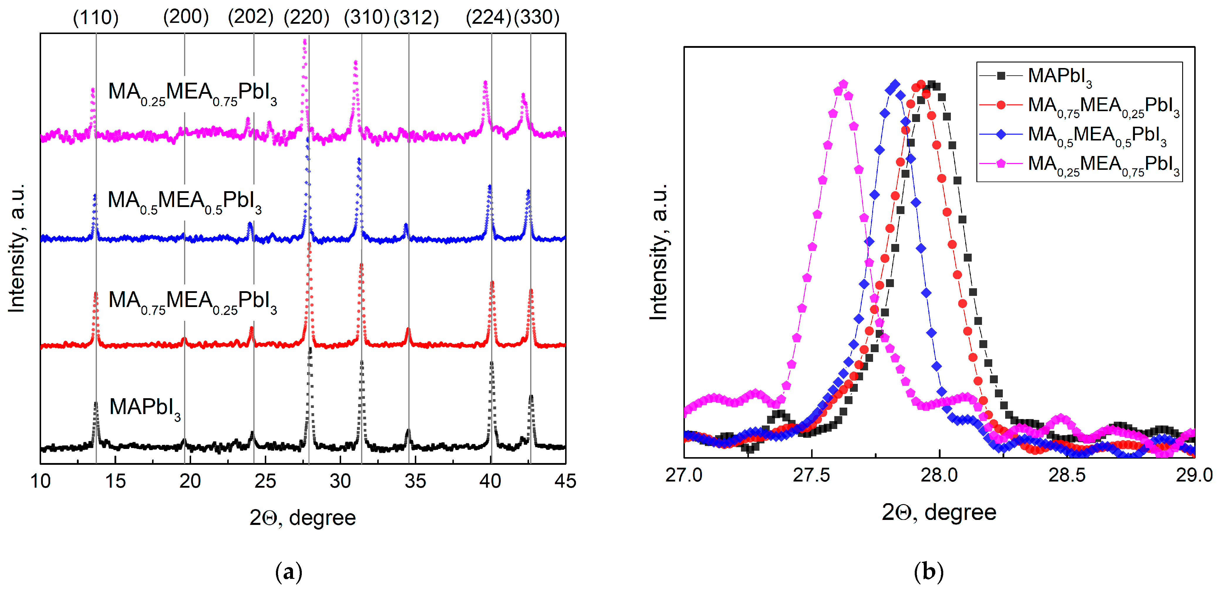
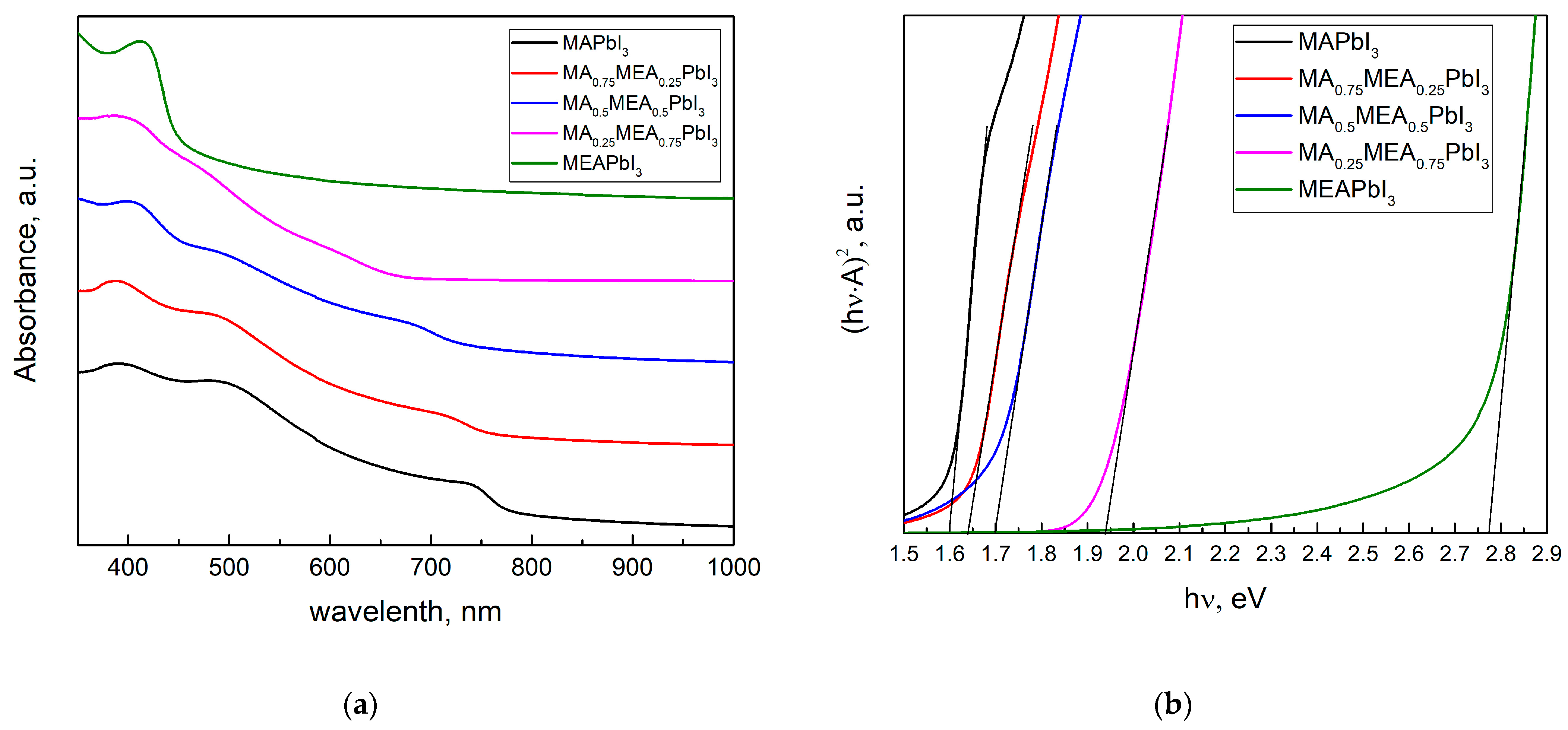
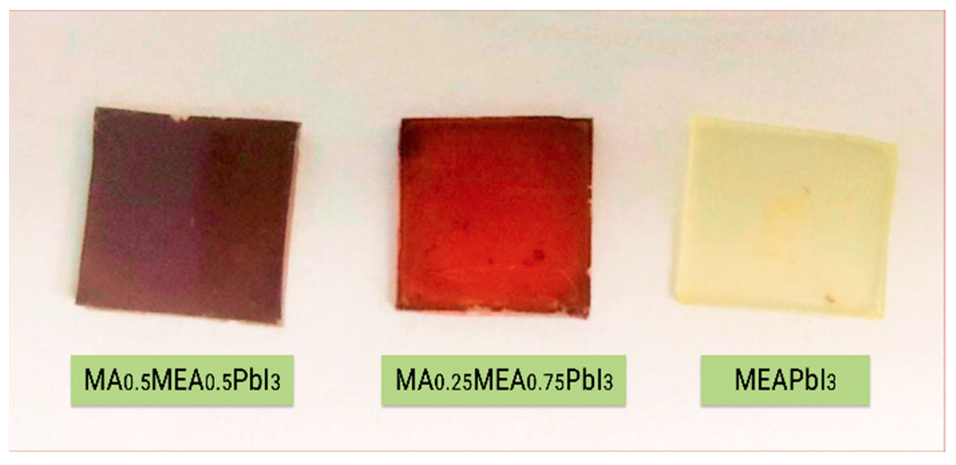
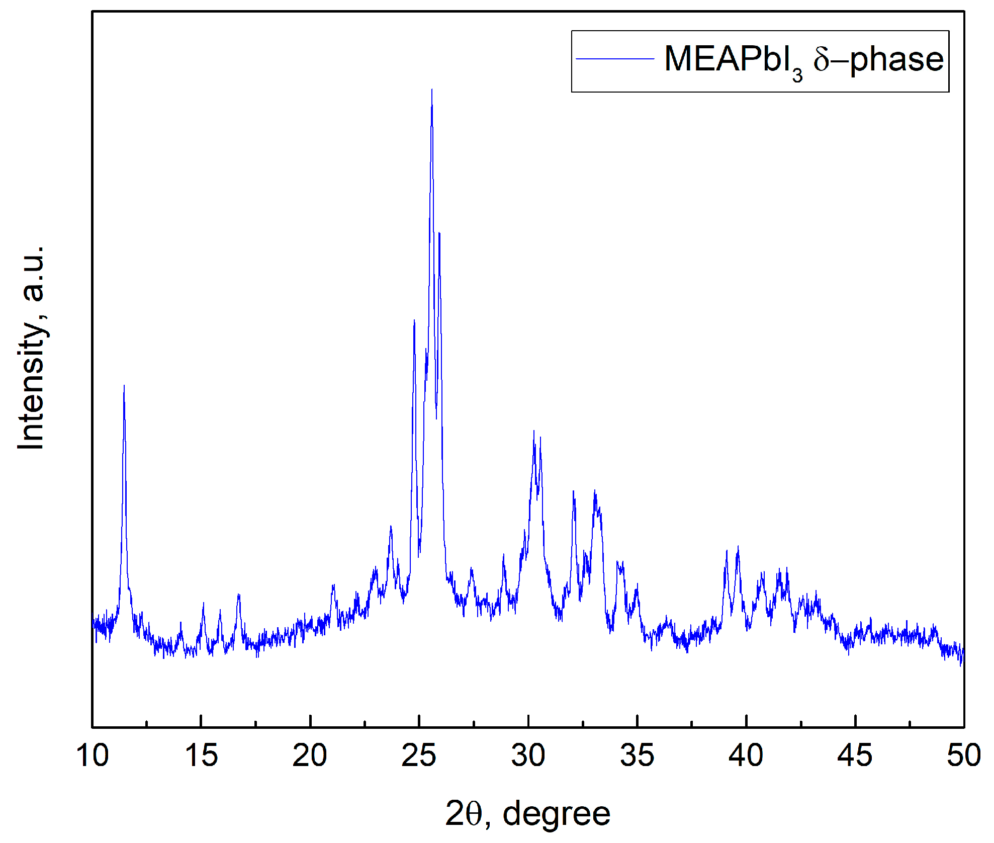
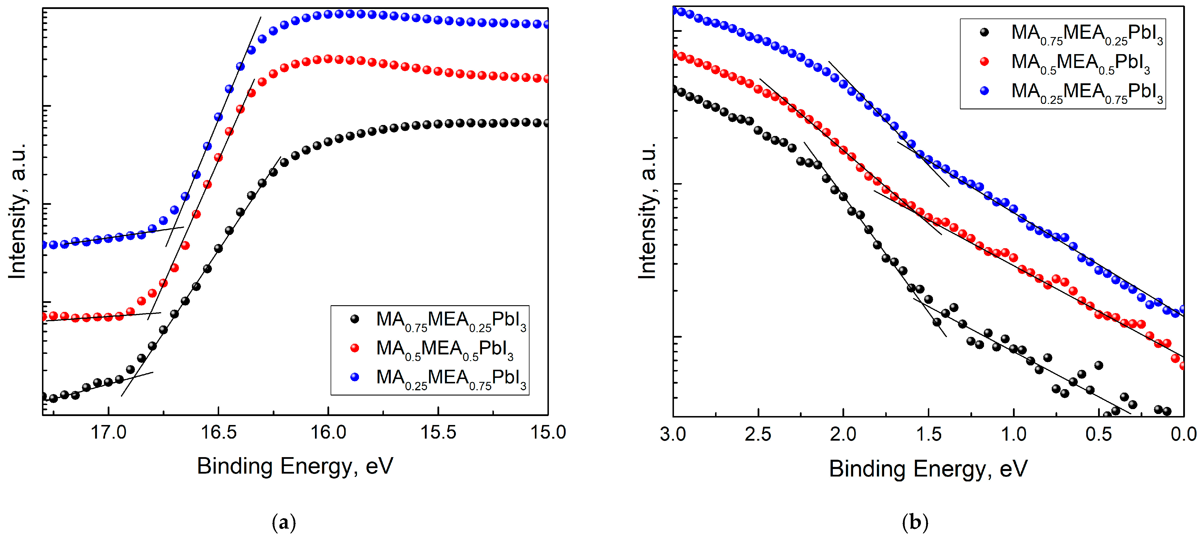
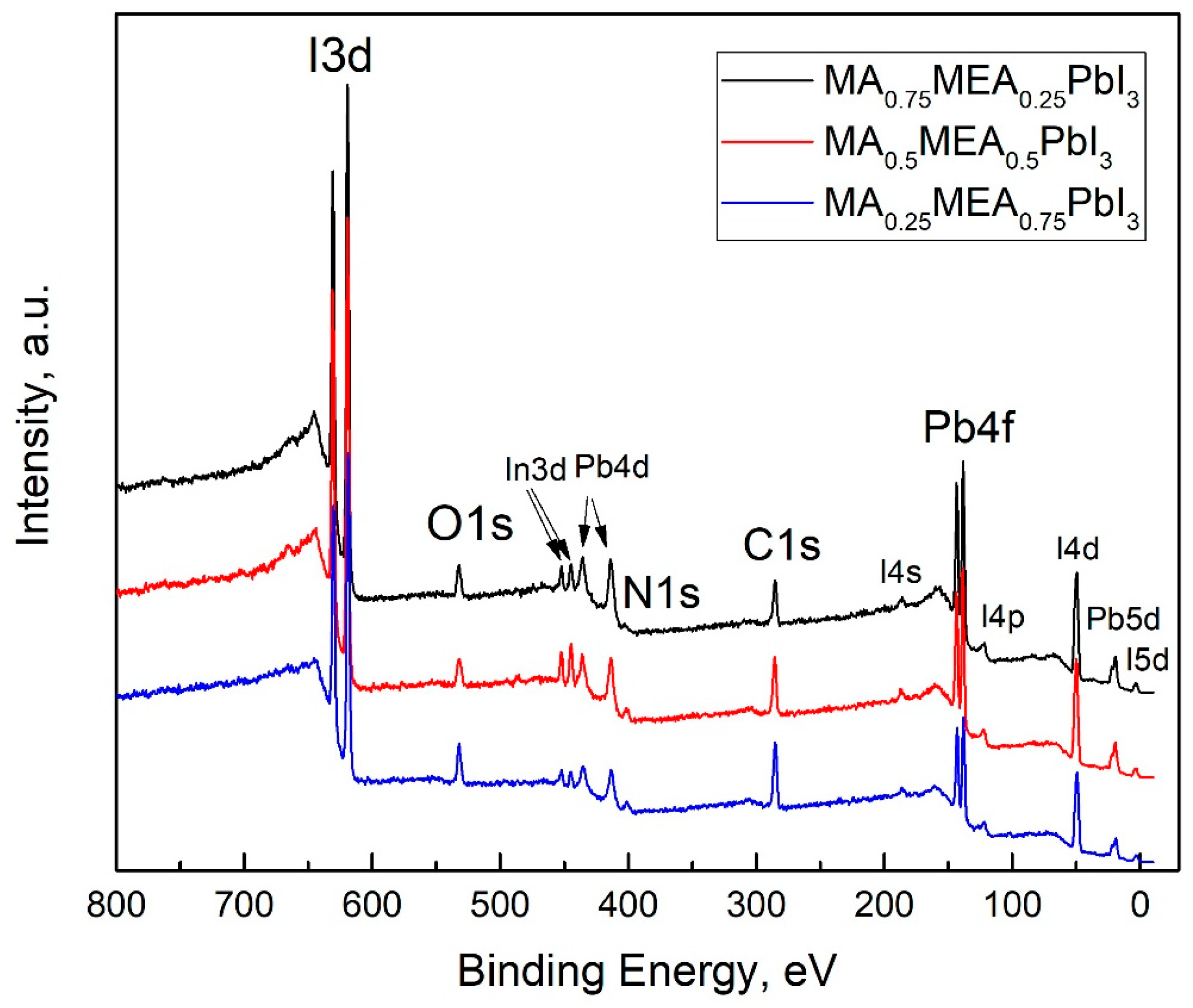
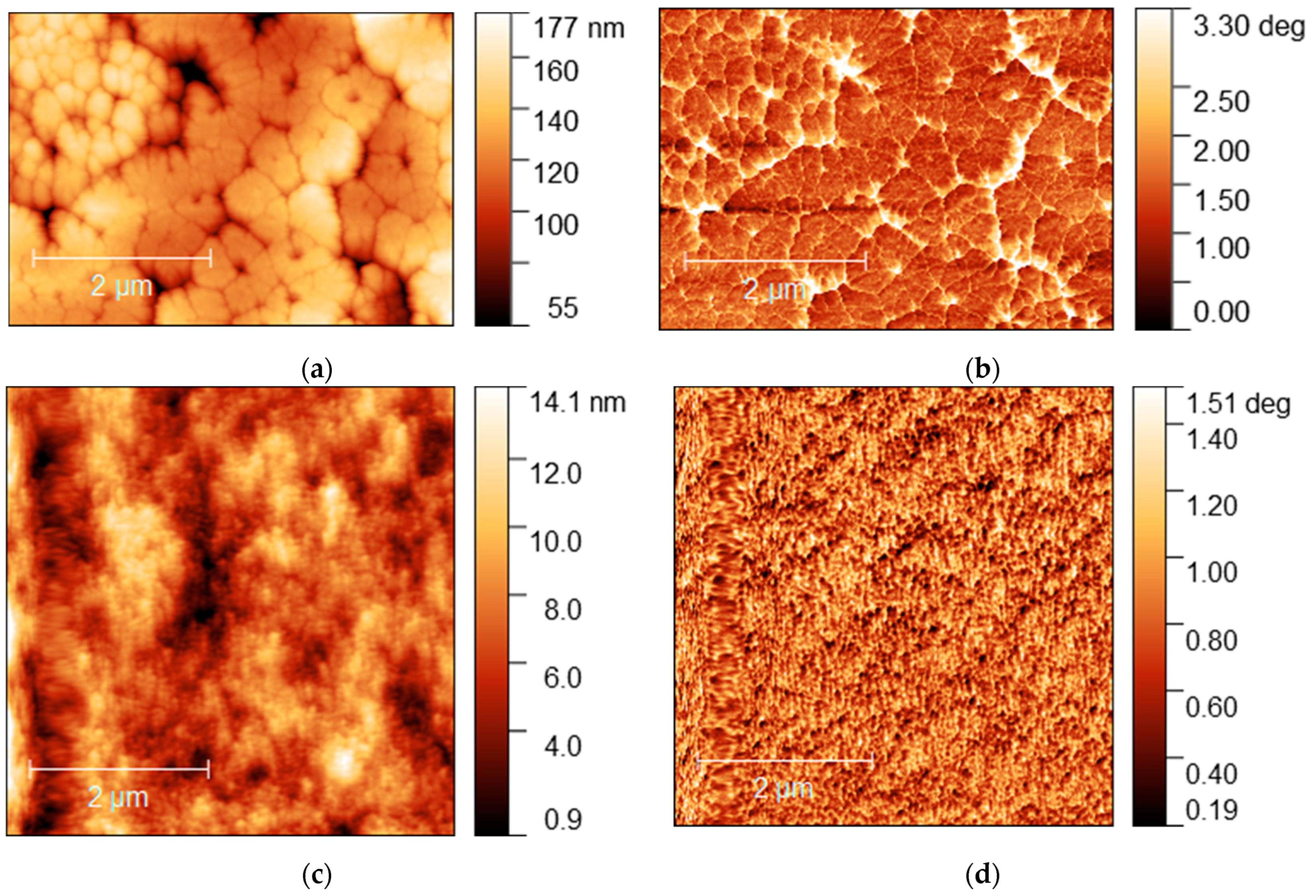
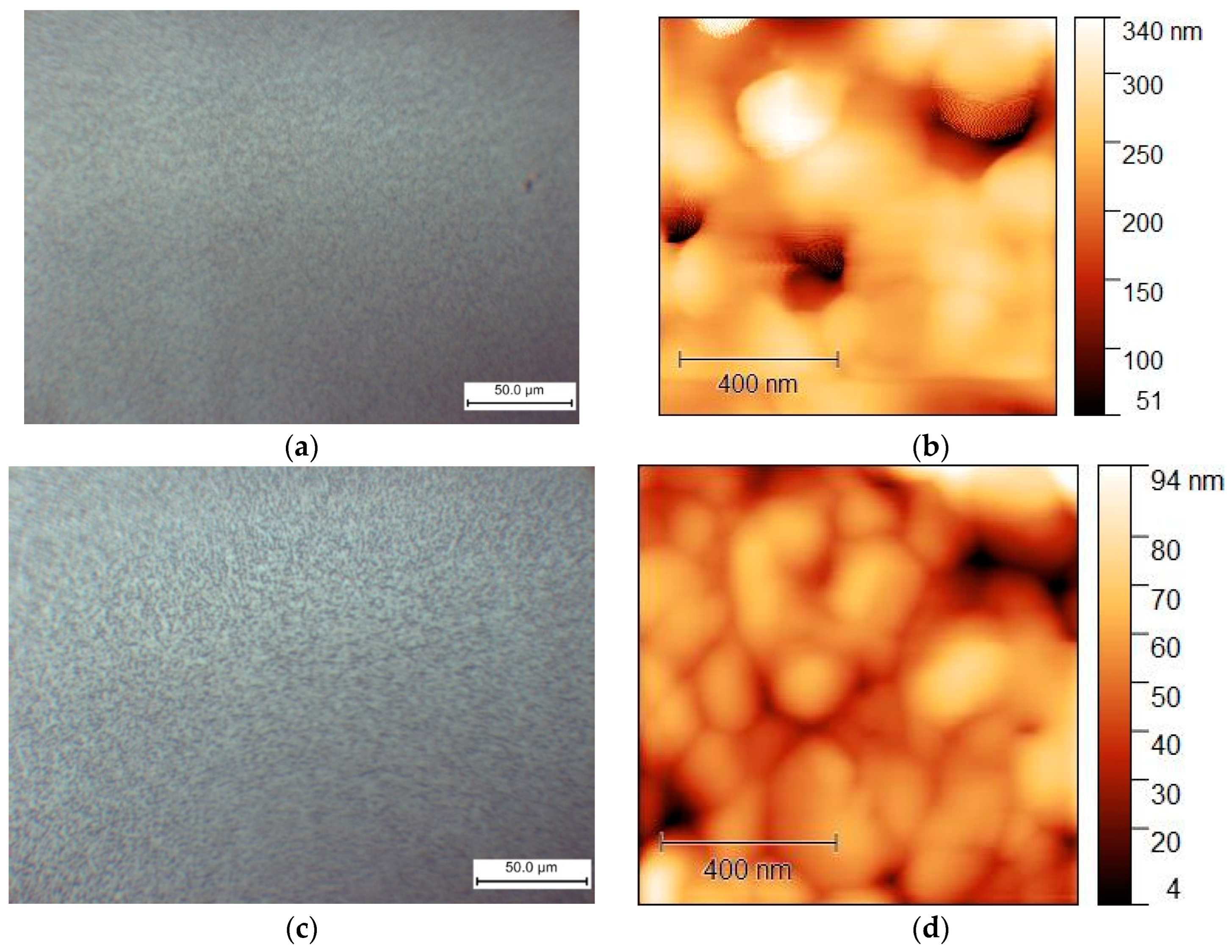
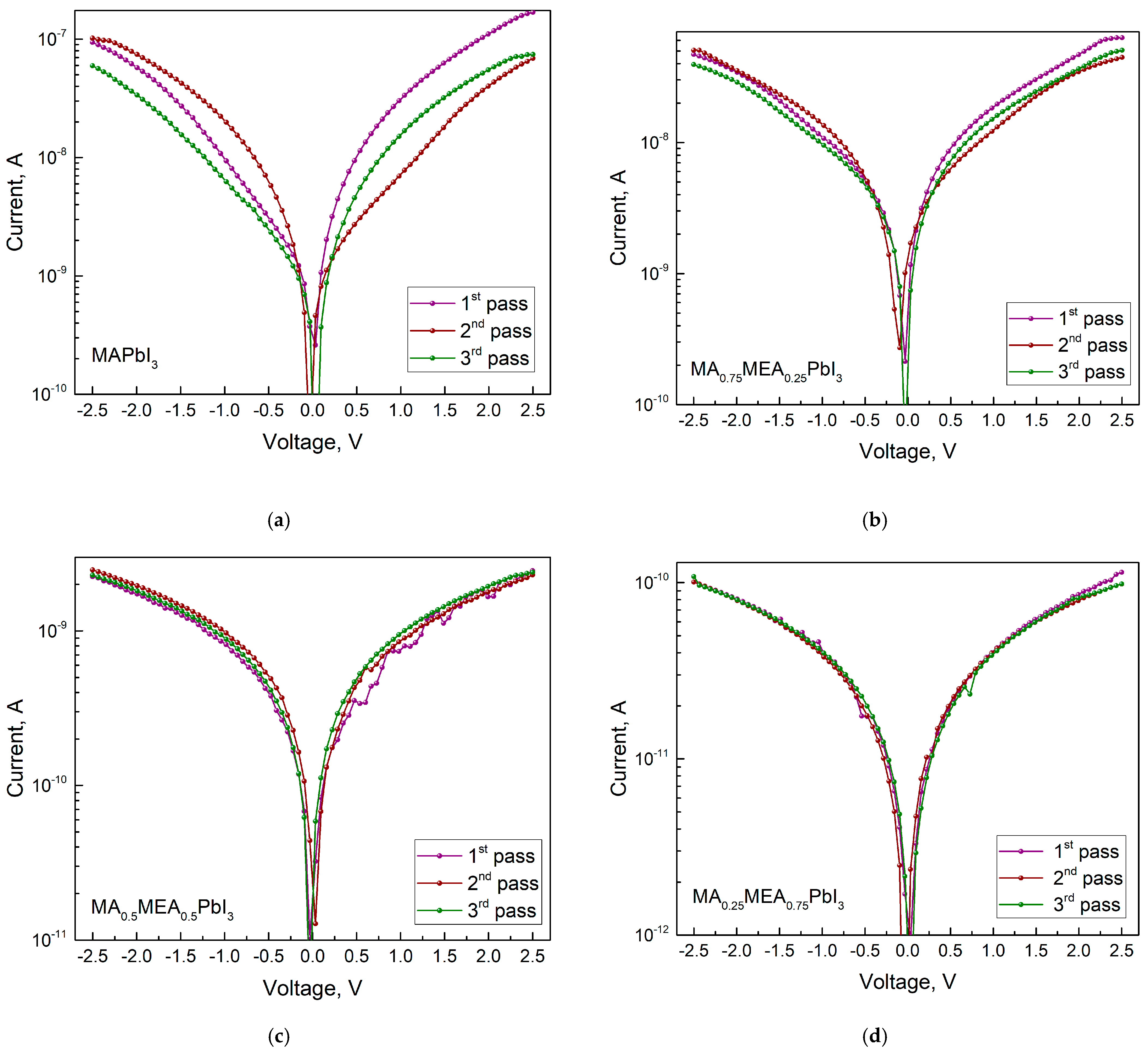
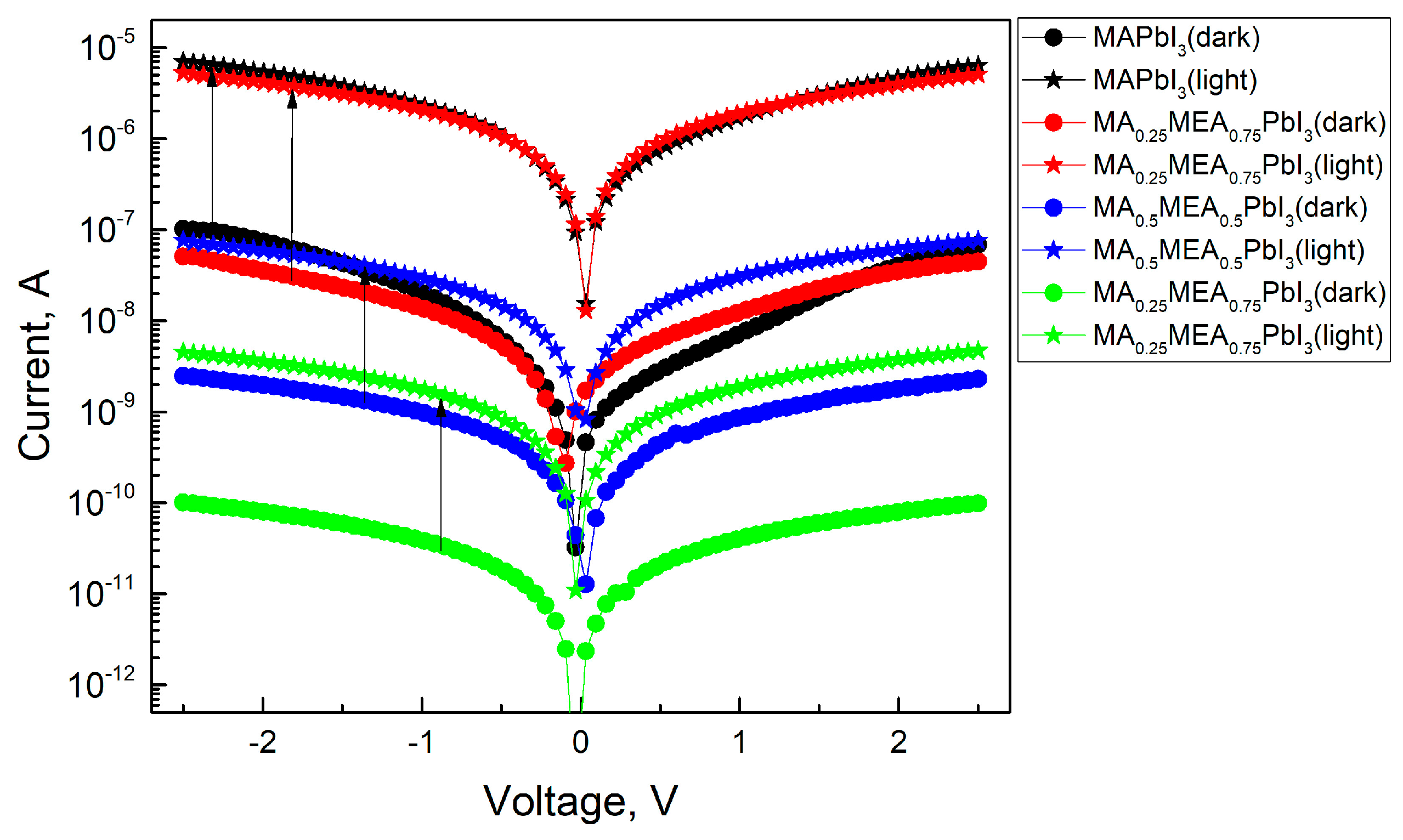
3. Results and Discussion

Figure 1a displays the XRD patterns for the perovskites MA0.25MEA0.75PbI3, MA0.5MEA0.75PbI3, MA0.75MEA0.25PbI3, and MAPbI3. The obtained samples confirmed the tetragonal structure of the obtained perovskites with minor peaks of planes (200), (202), and (312), and intense peaks assigned to planes (110), (220), (310), (224), and (330) [44,50].
As the MEA fraction increases, XRD peaks shift to lower 2Θ angles, indicating expanded interplanar spacing. This correlates with a blue shift in the absorption edge and an increase in bandgap energy. This trend is clearly demonstrated in Figure 1b, which focuses on the (220) plane, the most intense peak in the samples. The systematic peak shift to lower 2Θ values with higher MEA concentration confirms the lattice expansion. These results suggest that the MAxMEA1−xPbI3 perovskites remain structurally stable across the studied composition range.
The data obtained in our study are in good agreement with the results presented in the work by Leblanc et al. [44]. In the aforementioned study, the crystal structure of the hybrid perovskite was thoroughly investigated using MA+ and MEA+ cations (in combination with Pb2+ and I), confirming the formation of a three-dimensional (3D) hybrid perovskite with a tetragonal structure. It was demonstrated that an increase in the proportion of the MEA+ cation leads to a decrease in the 2Θ angles for the main peaks, indicating an expansion of interplanar distances. Notably, in our independent study, the goal was not to intentionally reduce the proportion of Pb2+ and I to obtain compounds of the composition (MA)1−2.48x(MEA)3.48x[Pb1−xI3−x]; however, the obtained results demonstrate good consistency with the data from [44].
To calculate the effective tolerance factor (teff) for compositions of the type AxB1−xX3 (in our case, MAxMEA1−xPbI3), a previously proposed approach based on the calculation of the effective cation size (reff) can be used [51]. Specifically, the calculation of teff for the perovskites MAPbI3, MA0.75MEA0.25PbI3, MA0.5MEA0.5PbI3, MA0.25MEA0.75PbI3, and MEAPbI3 was performed using the following formulas:
r e f f = x · r M A + + ( 1 x ) · r M E A +
t e f f = r e f f + r I 2 · ( r P b 2 + + r I )
The ionic radii were assumed to be 0.132 nm for Pb2+, 0.206 nm for I, 0.18 nm for MA+, and 0.24 nm for MEA+ [52,53]. The calculated values of the effective tolerance factor (teff) were 0.81, 0.84, 0.87, 0.90, and 0.93 for the perovskites MAPbI3, MA0.75MEA0.25PbI3, MA0.5MEA0.5PbI3, MA0.25MEA0.75PbI3, and MEAPbI3, respectively. This approach demonstrates that the size of the MEA+ cation may be suitable for the formation of a perovskite crystal structure, providing an effective tolerance factor within the range of 0.8 to 1. However, the use of MEA+ may lead to the formation of intermolecular hydrogen bonds due to interactions of the NH3+···OH type [41]. In our view, the likelihood of hydrogen bond formation between cations such as MEA+ and MA+, as well as between MEA+ and MEA+ cations, may contribute to the formation of a 3D hybrid perovskite with channels in the crystal structure (deficiency of Pb2+ and I), which is consistent with the results described by Leblanc et al. [44].
Figure 2a displays the perovskite film’s absorption spectra. The absorption edge of MAxMEA1−xPbI3 shifts towards shorter wavelengths (blue shift) as the MEA fraction increases, indicating an increase in the bandgap energy (Figure 2b).
The optical bandgap Eg was determined in the Tauc coordinates (A·hν)1/r from hν by extrapolating the linear section to the energy coordinate, where r is determined by the type of dependence of the absorption coefficient of the semiconductor on the irradiation energy greater than the bandgap. For direct-gap semiconductors, the absorption coefficient is described by the root dependence (r = 1/2) [54]. The absorption spectrum remains nearly unchanged (Figure 2a), and the bandgap energy does not significantly increase even when MEA cations constitute up to 25% of the total cation concentration, as shown by UV–vis spectra in Tauc plot in Figure 2b. Therefore, incorporating MEA cations in MAxMEA1−xPbI3 up to x = 0.25 does not significantly reduce the material’s absorption of solar radiation. For MA0.25MEA0.75PbI3, a notable increase in the bandgap Eg = 1.94 eV was observed. These data are consistent with the increase in the interplanar distances in the MAxMEA1−xPbI3 crystal lattices. The shift of peaks in MA0.75MEA0.25PbI3 and MA0.5MEA0.5PbI3 to the region of smaller 2Θ angles is less noticeable than the shift of peaks in MA0.25MEA0.75PbI3, as illustrated in Figure 1b. The interplanar spacing of the crystal lattice and the bandgap energy (Eg) exhibit a nonlinear dependence on the MEA cation fraction in MAxMEA1−xPbI3. A similar sharp increase in the optical bandgap, observed for the perovskite MA0.25MEA0.75PbI3 (Eg ≈ 1.94 eV), was also recorded for the composition (MEA)0.73(MA)0.47[Pb0.80I2.80] (Eg ≈ 1.84 eV), which is structurally the closest. In this case, Pb2+ and I ions are absent in the channels of the crystal lattice, and the increase in the bandgap in the proposed model of the crystal structure is explained by the disruption of connectivity in the PbI6 octahedra along the crystallographic directions 2a + b and a − 2b [44]. This model of the crystal structure is of significant interest and can be considered a promising approach to explaining the observed phenomena. Overall, our results, demonstrating an increase in the bandgap with the expansion of interplanar distances in the 3D hybrid perovskite MAxMEA1−xPbI3, are consistent with previously obtained data and confirm their reliability.
Similar results regarding the formation of a 3D-vacant perovskite structure with a tetragonal crystal lattice were observed in the MEAxFA1−xSnI3 system for x = 0.6–1.0. For x = 0–0.2, an orthorhombic crystal structure was observed, while for x = 0.2–0.4, a rhombohedral structure was identified [55]. It can be hypothesized that in the MAxMEA1−xPbI3 system, there is a competition between the incorporation of the MEA+ cation into the crystal lattice and the formation of channels within the structure, depending on the proportion of MEA+ as well as the ratios of Pb2+ and I. The significant increase in the bandgap from Eg ≈ 1.7 eV for MA0.5MEA0.5PbI3 to Eg ≈ 1.94 eV for MA0.25MEA0.75PbI3 may also be attributed to the formation of channels induced by the high proportion of MEA+. These hypotheses require further comprehensive studies, including both theoretical calculations and direct observation of channels in the crystal structure, which is beyond the scope of this work.
The value of the bandgap Eg ≈ 1.7 eV for MA0.5MEA0.5PbI3 is in the range of preferred Eg values for the perovskite film in the top photovoltaic structure in silicon-based tandem solar cells [56,57]. The bandgap energy of MAxMEA1−xPbI3 can be tuned from approximately 1.6 eV (for x = 1, pure MAPbI3) to 1.94 eV (for x = 0.25, MA0.25MEA0.75PbI3), making it possible to optimize the material for specific applications, such as tandem solar cells.
Analysis of the absorption spectra indicates a notable shift in the absorption edge of MEAPbI3 relative to the MAxMEA1−xPbI3 samples, with an optical bandgap of ~2.77 eV. This value exceeds the bandgap energies of both the two-dimensional perovskite MEA2PbI4 and PbI2 [41,58]. As depicted in Figure 3, the MEAPbI3 film displayed a distinct yellow coloration. Additionally, the XRD patterns (Figure 4) suggest the formation of a non-perovskite phase, indicating that MEAPbI3 does not crystallize into the conventional perovskite structure under these conditions.
The CsPbI3 samples without additives exhibited similar behavior, forming an orthorhombic (δ) phase with identical XRD peak positions and no perovskite crystal structure [59]. Under certain conditions, hybrid perovskites incorporating common cations such as MA and FA can also adopt the δ-phase [60,61]. Thus, despite the fact that the effective tolerance factor (teff) for the MEAPbI3 compound is less than 1, the increased bandgap compared to PbI2, along with the XRD data, suggests the formation of the δ-phase in MEAPbI3. However, the primary conclusion of this study is that MEAPbI3 adopts a non-perovskite structure under the given experimental conditions.
For MA0.75MEA0.25PbI3, MA0.5MEA0.5PbI3, and MA0.25MEA0.75PbI3 organic–inorganic perovskites, the cutoff values for the high binding energy (Ecutoff) and the initial binding energy (Eonset) were determined (Figure 5). With the irradiation energy of 21.21 eV subtracted from Ecutoff, the work functions (Fermi level EF relative to vacuum) for the perovskites were A(MA0.75MEA0.25PbI3) = 4.33 eV, A(MA0.5MEA0.5PbI3) = 4.40 eV, and A(MA0.25MEA0.75PbI3) = 4.51 eV, respectively. To determine the value of the valence band maximum (VBM) relative to vacuum, the value of the initial binding energy (Eonset) was added to the work function A, that is, the following formula was used:
−VBM = hν − (Ecutoff − Eonset).
The VBM calculated values were 5.87 eV, 5.96 eV, and 6.07 eV for MA0.75MEA0.25PbI3, MA0.5MEA0.5PbI3, and MA0.25MEA0.75PbI3, respectively.
The EF values from UPS and the optical bandgap Eg values were used to construct the energy band diagram for MA0.75MEA0.25PbI3, MA0.5MEA0.5PbI3, and MA0.25MEA0.75PbI3 (Figure 6).
The VBM and EF values for MA0.75MEA0.25PbI3 are very close to MAPbI3 [62,63]. This similarity may be attributed to the insignificant influence of the small fraction of MEA cations on the lattice structure, band structure, and crystal lattice parameters. The Fermi level EF is also influenced by deviations in the perovskite composition from its stoichiometric ratio (i.e., the atomic ratio N:Pb:I). In the case of MA0.75MEA0.25PbI3, our measurements revealed a significant excess of Pb atoms relative to N and a slight deficiency of I atoms compared to Pb. Such deviations can induce n-type self-doping, likely due to the formation of electron-donating defects associated with Pb excess and I vacancies [64]. It is worth noting that the samples were briefly exposed to air prior to XPS analysis, which may have contributed to the partial evaporation of methylamine. For MA0.5MEA0.5PbI3, an excess of Pb was also detected, though it was less pronounced than in MA0.75MEA0.25PbI3. In contrast, the atomic ratio of N:Pb:I in MA0.25MEA0.75PbI3 was found to be closest to the stoichiometric ratio of 1:1:3. On the survey X-ray photoelectron spectroscopy (XPS) spectra presented in Figure 7, the most intense peaks corresponding to the core levels of I3d, Pb4f, N1s, C1s, and O1s are indicated. Additionally, less intense peaks are marked, with their identification carried out in accordance with the literature data [65,66,67].
It should also be noted that the UPS data of perovskite films are highly sensitive to experimental conditions, particularly the choice of substrate and film thickness. These factors can induce Fermi-level pinning, which may significantly affect the measured electronic properties [68]. The peaks of the In3d core level are associated with the ITO material at the grain boundaries of the thin films. Accordingly, the peak of the O1s core level is attributed not only to the presence of the OH group in the MEA+ cation but also to the oxygen of ITO, as well as the possible presence of adsorbed OH groups on the surface of the samples.
The morphology of the films formed on the glass substrate is significantly influenced by the MEAI content in the solution, as demonstrated by the optical microscopy results (Figure 8). Therefore, it is anticipated that the MEAI concentration will have a significant impact under other film acquisition conditions.
When perovskite films are deposited without the use of an antisolvent, the MAPbI3 film forms as elongated split crystalline (or dendritic structures) with a length of about 25 μm (Figure 8a). The formation of MAPbI3 elongated split crystals may also be observed in DMF without the addition of DMSO [69,70]. During the crystallization of MAPbI3, homogeneous nucleation in the near-surface region of a thin film of the solution is associated with the formation of such structures in [69]. As shown in Figure 8, the addition of MEAI to the solution has a significant effect on the morphology of the film. The size of the elongated split perovskite crystallites thus increases sharply to a characteristic size of 0.1–0.2 mm at 25% MEAI and 75% MAI (Figure 8b). These structures’ extremely high relief makes them unsuitable for the production of solar cells, but they might be useful for building planar structures and for applications as X-ray or photodetectors. Increasing the MEAI fraction further produces a continuous homogenous coating and layers devoid of dendritic structures.
A significant difference in morphology was also observed by AFM of samples MA0.5MEA0.5PbI3 and MA0.25MEA0.75PbI3 (Figure 9).
The MA0.5MEA0.5PbI3 film has a hierarchical structure, with larger grains (0.5–1 μm) made up of 50 nm nanocrystallites (Figure 9a,b). And the perovskite film MA0.25MEA0.75PbI3 is an even more uniform coating of 50 nm nanocrystallites (Figure 9c,d). Thus, a change in the concentration of MEAI obviously significantly affects the crystallization processes of perovskite films. The relief of the film MA0.5MEA0.5PbI3 is about 150 nm, while the relief of MA0.25MEA0.75PbI3 is around 15 nm (for an approximate film thickness of 400–500 nm). This leads to the fact that visually the surface of the film MA0.25MEA0.75PbI3 looks mirror-like. Thus, MA0.5MEA0.5PbI3 and MA0.25MEA0.75PbI3 films using DMF and DMSO (4:1) as a solvent are formed as continuous homogeneous coatings, which can be used to create perovskite solar cells without using an antisolvent.
When using an antisolvent (ethyl acetate), the MAPbI3 and MA0.75MEA0.25PbI3 films also become continuous and homogeneous, as shown in Figure 10.
The MAPbI3 and MA0.75MEA0.25PbI3 films demonstrate comparable surface morphology and are free of dendritic structures. Therefore, MA0.75MEA0.25PbI3 films deposited using an antisolvent (EA) are suitable for perovskite solar cell fabrication. This is significant because an MEA cation fraction x < 0.25 does not significantly alter the absorption spectrum, as demonstrated in the previous results.
The conductivity decreases as the MEA fraction (x) rises, as can be seen from the IV curves (Figure 11). Since the hybrid perovskite with a higher MEA proportion has a larger bandgap, this is an expected outcome. For MA0.75MEA0.25PbI3 the conductivity decreases insignificantly from the conductivity of MAPbI3, but a decrease in the IV hysteresis is observed.
As the MEA fraction increases, the hysteresis (difference in current values under forward and reverse voltage sweeps) decreases. The hysteresis in IV characteristics of hybrid perovskites arises from ion migration [71,72]. Thus, the reduced IV hysteresis in MAxMEA1−xPbI3 suggests improved stability in solar cells and photodetectors. IV measurements under green LED irradiation (Figure 12) reveal that all MAxMEA1−xPbI3 polycrystalline layers demonstrate strong photoresponse.
A slight decrease in the photoresponse with increasing MEA can be attributed to changes in the absorption spectrum of the samples. This trend would also be observed under irradiation with a solar radiation simulator. Nevertheless, the hybrid perovskite MAxMEA1−xPbI3 retains the strong photoresponse typical of hybrid perovskites, alongside a significant reduction in the hysteresis of the I–V characteristics.

4. Conclusions

In this study, hybrid 3D perovskites were synthesized using the monoethanolammonium cation. The resulting hybrid perovskites, MAxMEA1−xPbI3 (with MEA fraction up to 1 − x = 0.75), crystallize in a tetragonal perovskite structure. It was found that the MEAPbI3 compound does not form a stable perovskite phase without the addition of other cations.
An increase in the MEA fraction leads to a shift in the XRD peaks towards smaller 2Θ angles, indicating an expansion of the lattice parameters. Concurrently, changes in the bandgap and the shape of the absorption spectra were observed. For the hybrid perovskites MA0.75MEA0.25PbI3, MA0.5MEA0.5PbI3, MA0.25MEA0.75PbI3, the energy levels were determined. The experimental results suggest that these perovskites are compatible with widely used electron and hole transport layers. Hybrid perovskites MA0.5MEA0.5PbI3 and MA0.25MEA0.75PbI3 (and similar compositions) are promising materials for use in tandem solar cells. In particular, the bandgap of MA0.5MEA0.5PbI3 Eg ≈ 1.7 eV makes this hybrid perovskite optimal in terms of Eg value for use in tandem solar cells with Si.
Perovskites MA0.5MEA0.5PbI3 and MA0.25MEA0.75PbI3 form homogeneous, continuous polycrystalline layers when spin-coated from a DMF:DMSO (4:1) solution. Monoethanolammonium iodide in solution significantly affects the morphology of polycrystalline perovskite layers. The hybrid perovskite MAxMEA1−xPbI3 exhibits minimal hysteresis in the I–V characteristics, which indicates reduced ion migration. This suggests improved stability for devices such as solar cells, photodetectors, and X-ray detectors.
For a small fraction of MEA (x ≤ 0.25), changes in the crystal structure, absorption spectrum, and bandgap are minimal. However, a reduction in I–V hysteresis is observed, suggesting lower degradation in solar cells without compromising solar absorption. This work provides foundational insights into the synthesis and properties of 3D hybrid perovskites incorporating the monoethanolammonium cation.

Author Contributions

Conceptualization, A.R., A.T., E.M., I.V., A.A. and V.M.; methodology A.R., M.O., A.T., O.K., A.M., A.K. and E.L.; software, A.K. and E.L.; validation A.R., M.O., A.K., I.V., A.A. and V.M.; formal analysis A.R., I.V., A.A. and V.M.; investigation, A.R., M.O., O.K. (XRD measurements), A.M. (AFM measurements), A.K. and E.L.; resources A.R., A.K., E.M., I.V., A.A. and V.M.; data curation, A.R., M.O., E.M. and A.A.; writing—original draft preparation, A.R. and M.O.; writing—review and editing, A.R., M.O., I.V. and A.A.; visualization, A.R.; supervision, I.V., A.A. and V.M.; project administration, A.R. and E.M.; funding acquisition, E.M., I.V., A.A. and V.M. All authors have read and agreed to the published version of the manuscript.

Funding

The work was carried out with the support of a grant from Russian Science Foundation No. 23-42-10029 dated 20 December 2022, https://rscf.ru/en/project/23-42-10029/. This research was funded by the Belarusian Republican Foundation for Fundamental Research grant number F23RNF-160.

Data Availability Statement

Data are contained within the article.

Acknowledgments

The XPS and UPS measurements were conducted using the equipment of the Research Park of St. Petersburg State University “Centre for Physical methods of surface investigation”.

Conflicts of Interest

The authors declare no conflicts of interest.

References

  1. Shen, Z.; Han, Q.; Luo, X.; Shen, Y.; Wang, Y.; Yuan, Y.; Zhang, Y.; Yang, Y.; Han, L. Efficient and Stable Perovskite Solar Cells with Regulated Depletion Region. Nat. Photonics 2024, 18, 450–457. [Google Scholar] [CrossRef]
  2. Khatoon, S.; Yadav, S.K.; Chakraborty, V.; Singh, J.; Singh, R.B.; Hasnain, M.S.; Hasnain, S.M.M. Perovskite Solar Cell’s Efficiency, Stability and Scalability: A Review. Mater. Sci. Energy Technol. 2023, 6, 437–459. [Google Scholar] [CrossRef]
  3. Wang, J.; Zhang, J.; Zhou, Y.; Liu, H.; Xue, Q.; Li, X.; Chueh, C.-C.; Yip, H.-L.; Zhu, Z.; Jen, A.K.-Y. Highly Efficient All-Inorganic Perovskite Solar Cells with Suppressed Non-Radiative Recombination by a Lewis Base. Nat. Commun. 2020, 11, 117. [Google Scholar] [CrossRef]
  4. Xiang, W.; Liu, S.; Tress, W. A Review on the Stability of Inorganic Metal Halide Perovskites: Challenges and Opportunities for Stable Solar Cells. Energy Environ. Sci. 2021, 14, 2090–2113. [Google Scholar] [CrossRef]
  5. Mali, S.S.; Patil, J.V.; Steele, J.; Nazeeruddin, M.K.; Kim, J.H.; Hong, C.K. All-Inorganic Halide Perovskites for Air-Processed “N–I–P” Monolithic Perovskite/Organic Hybrid Tandem Solar Cells Exceeding 23% Efficiency. Energy Environ. Sci. 2024, 17, 1046–1060. [Google Scholar] [CrossRef]
  6. Matyushkin, L.B.; Moshnikov, V.A. Photoluminescence of Perovskite CsPbX3 (X = Cl, Br, I) Nanocrystals and Solid Solutions on Their Basis. Semiconductors 2017, 51, 1337–1342. [Google Scholar] [CrossRef]
  7. Ye, H.-Y.; Tang, Y.-Y.; Li, P.-F.; Liao, W.-Q.; Gao, J.-X.; Hua, X.-N.; Cai, H.; Shi, P.-P.; You, Y.-M.; Xiong, R.-G. Metal-Free Three-Dimensional Perovskite Ferroelectrics. Science 2018, 361, 151–155. [Google Scholar] [CrossRef]
  8. Song, X.; Hodes, G.; Zhao, K.; Liu, S. Metal-Free Organic Halide Perovskite: A New Class for next Optoelectronic Generation Devices. Adv. Energy Mater. 2021, 11, 2003331. [Google Scholar] [CrossRef]
  9. Cho, S.H.; Jung, Y.; Jang, Y.-W.; Kim, H.; Kim, J.; Lim, C.; Park, K.-T.; Kim, S.; Chu, Y.H.; Kim, T.; et al. Fabrication Strategies for 2D Halide Perovskite Towards Next-Generation Optoelectronic Applications. Int. J. Precis. Eng. Manuf. Green Technol. 2024, 12, 349–380. [Google Scholar] [CrossRef]
  10. Kostopoulou, A.; Konidakis, I.; Stratakis, E. Two-Dimensional Metal Halide Perovskites and Their Heterostructures: From Synthesis to Applications. Nanophotonics 2023, 12, 1643–1710. [Google Scholar] [CrossRef]
  11. Yuan, Z.; Zhou, C.; Tian, Y.; Shu, Y.; Messier, J.; Wang, J.C.; Burgt, L.J.v.d.; Kountouriotis, K.; Xin, Y.; Holt, E.D.; et al. One-Dimensional Organic Lead Halide Perovskites with Efficient Bluish White-Light Emission. Nat. Commun. 2017, 8, 14051. [Google Scholar] [CrossRef]
  12. Tarasov, A. Band Gap and Topology of 1D Perovskite-Derived Hybrid Lead Halide Structures. Crystals 2022, 12, 657. [Google Scholar] [CrossRef]
  13. Mei, A.; Peng, X.; Li, X.; Zhang, G.; Lin, S.; Fu, N. Anions Regulation of 1D Perovskite Intrusion-Behavior for Efficient and Stable Perovskite Solar Cells. ACS Appl. Mater. Interfaces 2024, 16, 31209–31217. [Google Scholar] [CrossRef] [PubMed]
  14. Liu, X.; Wang, Y.; Wang, Y.; Zhao, Y.; Yu, J.; Shan, X.; Tong, Y.; Lian, X.; Wan, X.; Wang, L.; et al. Recent Advances in Perovskites-Based Optoelectronics. Nanotechnol. Rev. 2022, 11, 3063–3094. [Google Scholar] [CrossRef]
  15. Khan, J.; Zhang, X.; Yuan, J.; Wang, Y.; Shi, G.; Patterson, R.; Shi, J.; Ling, X.; Hu, L.; Wu, T.; et al. Tuning the Surface-Passivating Ligand Anchoring Position Enables Phase Robustness in CsPbI3 Perovskite Quantum Dot Solar Cells. ACS Energy Lett. 2020, 5, 3322–3329. [Google Scholar] [CrossRef]
  16. Li, X.; Aftab, S.; Hussain, S.; Kabir, F.; Henaish, A.M.A.; Al-Sehemi, A.G.; Pallavolu, M.R.; Koyyada, G. Dimensional diversity (0D, 1D, 2D, and 3D) in perovskite solar cells: Exploring the potential of mixed-dimensional integrations. J. Mater. Chem. A 2024, 12, 4421–4440. [Google Scholar] [CrossRef]
  17. Aleshin, A.N.; Shcherbakov, I.P.; Gushchina, E.V.; Matyushkin, L.B.; Moshnikov, V.A. Solution-Processed Field-Effect Transistors Based on Polyfluorene –Cesium Lead Halide Nanocrystals Composite Films with Small Hysteresis of Output and Transfer Characteristics. Org. Electron. 2017, 50, 213–219. [Google Scholar] [CrossRef]
  18. Krishna, B.G.; Ghosh, D.S.; Tiwari, S. Progress in Ambient Air-Processed Perovskite Solar Cells: Insights into Processing Techniques and Stability Assessment. Sol. Energy 2021, 224, 1369–1395. [Google Scholar] [CrossRef]
  19. Lian, Z.; Yan, Q.; Lv, Q.; Wang, Y.; Liu, L.; Zhang, L.; Pan, S.; Li, Q.; Wang, L.-D.; Sun, J.-L. High-Performance Planar-Type Photodetector on (100) Facet of MAPbI3 Single Crystal. Sci. Rep. 2015, 5, 16563. [Google Scholar] [CrossRef]
  20. Khan, F.; Rezgui, B.D.; Khan, M.T.; Al-Sulaiman, F.A. Perovskite-Based Tandem Solar Cells: Device Architecture, Stability, and Economic Perspectives. Renew. Sustain. Energy Rev. 2022, 165, 112553. [Google Scholar] [CrossRef]
  21. Li, H.; Zhang, W. Perovskite Tandem Solar Cells: From Fundamentals to Commercial Deployment. Chem. Rev. 2020, 120, 9835–9950. [Google Scholar] [CrossRef]
  22. Zhang, Y.; Zhang, H.; Zhang, X.; Wei, L.; Zhang, B.; Sun, Y.; Hai, G.; Li, Y. Major Impediment to Highly Efficient, Stable and Low-Cost Perovskite Solar Cells. Metals 2018, 8, 964. [Google Scholar] [CrossRef]
  23. Moshnikov, V.; Muratova, E.; Aleshin, A.; Maksimov, A.; Nenashev, G.; Vrublevsky, I.; Lushpa, N.; Tuchkovsky, A.; Zhilenkov, A.; Kichigina, O. Controlled Crystallization of Hybrid Perovskite Films from Solution Using Prepared Crystal Centers. Crystals 2024, 14, 376. [Google Scholar] [CrossRef]
  24. Ahmadi, M.; Wu, T.; Hu, B. A Review on Organic–Inorganic Halide Perovskite Photodetectors: Device Engineering and Fundamental Physics. Adv. Mater. 2017, 29, 1605242. [Google Scholar] [CrossRef]
  25. Kim, Y.C.; Kim, K.H.; Son, D.-Y.; Jeong, D.-N.; Seo, J.-Y.; Choi, Y.S.; Han, I.T.; Lee, S.Y.; Park, N.-G. Printable Organometallic Perovskite Enables Large-Area, Low-Dose X-Ray Imaging. Nature 2017, 550, 87–91. [Google Scholar] [CrossRef] [PubMed]
  26. Zhao, X.; Xu, H.; Wang, Z.; Lin, Y.; Liu, Y. Memristors with Organic-Inorganic Halide Perovskites. InfoMat 2019, 1, 183–210. [Google Scholar] [CrossRef]
  27. Zhu, X.; Lee, J.; Lu, W. Iodine Vacancy Redistribution in Organic–Inorganic Halide Perovskite Films and Resistive Switching Effects. Adv. Mater. 2017, 29, 1700527. [Google Scholar] [CrossRef]
  28. Nenashev, G.V.; Aleshin, A.N.; Shcherbakov, I.P.; Petrov, V.N. Effect of Temperature Variations on the Behavior of a Two-Terminal Organic–Inorganic Halide Perovskite Rewritable Memristor for Neuromorphic Operations. Solid State Commun. 2022, 348–349, 114768. [Google Scholar] [CrossRef]
  29. Bencherif, H.; Meddour, F.; Elshorbagy, M.H.; Hossain, M.K.; Cuadrado, A.; Abdi, M.A.; Bendib, T.; Kouda, S.; Alda, J. Performance Enhancement of (FAPbI3)1−x(MAPbBr3)x Perovskite Solar Cell with an Optimized Design. Micro Nanostruct. 2022, 171, 207403. [Google Scholar] [CrossRef]
  30. Gao, B.; Meng, J. RbCs(MAFA)PbI3 Perovskite Solar Cell with 22.81% Efficiency Using the Precise Ions Cascade Regulation. Appl. Surf. Sci. 2020, 530, 147240. [Google Scholar] [CrossRef]
  31. Fan, X. Advanced Progress in Metal Halide Perovskite Solar Cells: A Review. Mater. Today Sustain. 2023, 24, 100603. [Google Scholar] [CrossRef]
  32. Nenashev, G.V.; Aleshin, A.N.; Ryabko, A.A.; Shcherbakov, I.P.; Moshnikov, V.A.; Muratova, E.N.; Kondratev, V.M.; Vrublevsky, I.A. Effect of Barium Doping on the Behavior of Conductivity and Impedance of Organic-Inorganic Perovskite Films. Solid State Commun. 2024, 388, 115554. [Google Scholar] [CrossRef]
  33. Su, K.; Chen, W.; Huang, Y.; Yang, G.; Brooks, K.G.; Zhang, B.; Feng, Y.; Nazeeruddin, M.K.; Zhang, Y. In Situ Graded Passivation via Porphyrin Derivative with Enhanced Photovoltage and Fill Factor in Perovskite Solar Cells. Sol. RRL 2021, 6, 2100964. [Google Scholar] [CrossRef]
  34. Feng, W.; Tan, Y.; Yang, M.; Jiang, Y.; Lei, B.-X.; Wang, L.P.; Wu, W.-Q. Small Amines Bring Big Benefits to Perovskite-Based Solar Cells and Light-Emitting Diodes. Chem 2022, 8, 351–383. [Google Scholar] [CrossRef]
  35. Azmi, R.; Ugur, E.; Seitkhan, A.; Aljamaan, F.; Subbiah, A.S.; Liu, J.; Harrison, G.T.; Nugraha, M.I.; Eswaran, M.K.; Babics, M.; et al. Damp Heat–Stable Perovskite Solar Cells with Tailored-Dimensionality 2D/3D Heterojunctions. Science 2022, 376, 73–77. [Google Scholar] [CrossRef]
  36. Leung, T.L.; Ahmad, I.; Syed, A.A.; Ng, A.M.C.; Popović, J.; Chen, W. Stability of 2D and Quasi-2D Perovskite Materials and Devices. Commun. Mater. 2022, 3, 63. [Google Scholar] [CrossRef]
  37. Ahmad, S.; Fu, P.; Yu, S.; Yang, Q.; Liu, X.; Wang, X.; Wang, K.; Guo, X.; Li, C. Dion-Jacobson Phase 2D Layered Perovskites for Solar Cells with Ultrahigh Stability. Joule 2018, 3, 794–806. [Google Scholar] [CrossRef]
  38. Hsiao, K.-C.; Jao, M.-H.; Tian, K.-Y.; Lin, T.-H.; Tran, D.-P.; Liao, H.-C.; Hou, C.-H.; Shyue, J.-J.; Wu, M.-C.; Su, W.-F. Acetamidinium Cation to Confer Ion Immobilization and Structure Stabilization of Organometal Halide Perovskite toward Long Life and High-Efficiency P-I-N Planar Solar Cell via Air-Processable Method. Sol. RRL 2020, 4, 2070092. [Google Scholar] [CrossRef]
  39. Minussi, F.B.; Silva, R.M.; Moraes, J.C.S.; Araújo, E.B. Organic Cations in Halide Perovskite Solid Solutions: Exploring beyond Size Effects. Phys. Chem. Chem. Phys. 2024, 26, 20770–20784. [Google Scholar] [CrossRef]
  40. Singh, P.; Mukherjee, R.; Avasthi, S. Acetamidinium-Substituted Methylammonium Lead Iodide Perovskite Solar Cells with Higher Open-Circuit Voltage and Improved Intrinsic Stability. ACS Appl. Mater. Interfaces 2020, 12, 13982–13987. [Google Scholar] [CrossRef]
  41. Mercier, N.; Poiroux, S.; Riou, A.; Batail, P. Unique Hydrogen Bonding Correlating with a Reduced Band Gap and Phase Transition in the Hybrid Perovskites (HO(CH2)2NH3)2PbX4 (X = I, Br). Inorg. Chem. 2004, 43, 8361–8366. [Google Scholar] [CrossRef] [PubMed]
  42. Grancini, G.; Roldán-Carmona, C.; Zimmermann, I.; Mosconi, E.; Lee, X.; Martineau, D.; Narbey, S.; Oswald, F.; Angelis, F.D.; Grätzel, M.; et al. One-Year Stable Perovskite Solar Cells by 2D/3D Interface Engineering. Nat. Commun. 2017, 8, 15684. [Google Scholar] [CrossRef]
  43. Cheng, B.; Li, T.-Y.; Maity, P.; Wei, P.-C.; Nordlund, D.; Ho, K.-T.; Lien, D.-H.; Lin, C.-H.; Liang, R.-Z.; Miao, X.; et al. Extremely Reduced Dielectric Confinement in Two-Dimensional Hybrid Perovskites with Large Polar Organics. Commun. Phys. 2018, 1, 80. [Google Scholar] [CrossRef]
  44. Leblanc, A.; Mercier, N.; Allain, M.; Dittmer, J.; Fernandez, V.; Pauporté, T. Lead- and Iodide-Deficient (CH3NH3)PbI3 (D-MAPI): The Bridge between 2D and 3D Hybrid Perovskites. Angew. Chem. Int. Ed. 2017, 56, 16067–16072. [Google Scholar] [CrossRef]
  45. Parashar, M.; Kaul, A.B. Methylammonium Lead Tri-Iodide Perovskite Solar Cells with Varying Equimolar Concentrations of Perovskite Precursors. Appl. Sci. 2021, 11, 11689. [Google Scholar] [CrossRef]
  46. Ahmed, D.S.; Mohammed, B.K.; Mohammed, M.K.A. Long-Term Stable and Hysteresis-Free Planar Perovskite Solar Cells Using Green Antisolvent Strategy. J. Mater. Sci. 2021, 56, 15205–15214. [Google Scholar] [CrossRef]
  47. Ryabko, A.A.; Nalimova, S.S.; Permyakov, N.V.; Bobkov, A.A.; Maksimov, A.I.; Kondratev, V.M.; Kotlyar, K.P.; Ovezov, M.K.; Komolov, A.S.; Lazneva, E.F.; et al. Architectonics of Zinc Oxide Nanorod Coatings for Adsorption Gas Sensors. Tech. Phys. 2024, 69, 2103–2110. [Google Scholar] [CrossRef]
  48. Pronin, I.A.; Averin, I.A.; Karmanov, A.A.; Yakushova, N.D.; Komolov, A.S.; Lazneva, E.F.; Sychev, M.M.; Moshnikov, V.A.; Korotcenkov, G. Control over the Surface Properties of Zinc Oxide Powders via Combining Mechanical, Electron Beam, and Thermal Processing. Nanomaterials 2022, 12, 1924. [Google Scholar] [CrossRef]
  49. Komolov, A.S.; Lazneva, E.F.; Gerasimova, N.B.; Panina, Y.A.; Sobolev, V.S.; Koroleva, A.V.; Pshenichnyuk, S.A.; Asfandiarov, N.L.; Modelli, A.; Handke, B. Conduction Band Electronic States of Ultrathin Layers of Thiophene/Phenylene Co-Oligomers on an Oxidized Silicon Surface. J. Electron Spectrosc. Relat. Phenom. 2019, 235, 40–45. [Google Scholar] [CrossRef]
  50. Fan, P.; Gu, D.; Liang, G.; Luo, J.; Chen, J.; Zheng, Z.; Xie, D. High-Performance Perovskite CH3NH3PbI3 Thin Films for Solar Cells Prepared by Single-Source Physical Vapour Deposition. Sci. Rep. 2016, 6, 29910. [Google Scholar] [CrossRef]
  51. Li, Z.; Yang, M.; Park, J.-S.; Wei, S.-H.; Berry, J.J.; Zhu, K. Stabilizing Perovskite Structures by Tuning Tolerance Factor: Formation of Formamidinium and Cesium Lead Iodide Solid-State Alloys. Chem. Mater. 2015, 28, 284–292. [Google Scholar] [CrossRef]
  52. Jacobsson, T.J.; Correa-Baena, J.-P.; Pazoki, M.; Saliba, M.; Schenk, K.; Grätzel, M.; Hagfeldt, A. Exploration of the Compositional Space for Mixed Lead Halogen Perovskites for High Efficiency Solar Cells. Energy Environ. Sci. 2016, 9, 1706–1724. [Google Scholar] [CrossRef]
  53. McKinnon, N.K.; Reeves, D.C.; Akabas, M.H. 5-HT3 Receptor Ion Size Selectivity Is a Property of the Transmembrane Channel, Not the Cytoplasmic Vestibule Portals. J. Gen. Physiol. 2011, 138, 453–466. [Google Scholar] [CrossRef] [PubMed]
  54. Klein, J.; Kampermann, L.; Mockenhaupt, B.; Behrens, M.; Strunk, J.; Bacher, G. Limitations of the Tauc Plot Method. Adv. Funct. Mater. 2023, 33, 2304523. [Google Scholar] [CrossRef]
  55. Tsai, C.C.; Lin, Y.-P.; Pola, M.K.; Narra, S.; Jokar, E.; Yang, Y.-W.; Diau, E.W.-G. Control of Crystal Structures and Optical Properties with Hybrid Formamidinium and 2-Hydroxyethylammonium Cations for Mesoscopic Carbon-Electrode Tin-Based Perovskite Solar Cells. ACS Energy Lett. 2018, 3, 2077–2085. [Google Scholar] [CrossRef]
  56. Lal, N.; Dkhissi, Y.; Li, W.; Hou, Q.; Cheng, Y.-B.; Bach, U. Perovskite Tandem Solar Cells. Adv. Energy Mater. 2017, 7, 1602761. [Google Scholar] [CrossRef]
  57. Rajagopal, A.; Yao, K.; Jen, A.K.-Y. Toward Perovskite Solar Cell Commercialization: A Perspective and Research Roadmap Based on Interfacial Engineering. Adv. Mater. 2018, 30, 1800455. [Google Scholar] [CrossRef]
  58. Basumatary, P.; Agarwal, P. Photocurrent Transient Measurements in MAPbI3 Thin Films. J. Mater. Sci. Mater. Electron. 2020, 31, 10047–10054. [Google Scholar] [CrossRef]
  59. Ke, W.; Spanopoulos, I.; Stoumpos, C.C.; Kanatzidis, M.G. Myths and Reality of HPbI3 in Halide Perovskite Solar Cells. Nat. Commun. 2018, 9, 4785. [Google Scholar] [CrossRef]
  60. Finkler, J.A.; Goedecker, S. Experimental Absence of the Non-Perovskite Ground State Phases of MaPbI3 Explained by a Funnel Hopping Monte Carlo Study Based on a Neural Network Potential. Mater. Adv. 2022, 4, 184–194. [Google Scholar] [CrossRef]
  61. Elsayed, M.R.A.; Elseman, A.M.; Abdelmageed, A.A.; Hashem, H.M.; Hassen, A. Synthesis and Numerical Simulation of Formamidinium-Based Perovskite Solar Cells: A Predictable Device Performance at NIS-Egypt. Sci. Rep. 2023, 13, 10115. [Google Scholar] [CrossRef]
  62. Oleiki, E.; Javaid, S.; Lee, G. Impact of Fluorination on the Energy Level Alignment of an FNZnPc/MAPbI3 Interface. Nanoscale Adv. 2022, 4, 5070–5076. [Google Scholar] [CrossRef]
  63. Hong, K.; Kwon, K.C.; Choi, K.S.; Le, Q.V.; Kim, S.J.; Han, J.S.; Suh, J.M.; Kim, S.Y.; Sutter-Fella, C.M.; Jang, H.W. Strong Fermi-Level Pinning at Metal Contacts to Halide Perovskites. J. Mater. Chem. C 2021, 9, 15212–15220. [Google Scholar] [CrossRef]
  64. Wang, Q.; Shao, Y.; Xie, H.; Lyu, L.; Liu, X.; Gao, Y.; Huang, J. Qualifying Composition Dependent P and N Self-Doping in CH3NH3PbI3. Appl. Phys. Lett. 2014, 105, 163508. [Google Scholar] [CrossRef]
  65. Zhidkov, I.S.; Poteryaev, A.I.; Kukharenko, A.I.; Finkelstein, L.D.; Cholakh, S.O.; Akbulatov, A.F.; Troshin, P.A.; Chueh, C.-C.; Kurmaev, E.Z. XPS Evidence of Degradation Mechanism in CH3NH3PbI3 Hybrid Perovskite. J. Phys. Condens. Matter 2019, 32, 95501. [Google Scholar] [CrossRef] [PubMed]
  66. Wang, K.; Ecker, B.; Gao, Y. Photoemission Studies on the Environmental Stability of Thermal Evaporated MAPbI3 Thin Films and MAPbBr3 Single Crystals. Energies 2021, 14, 2005. [Google Scholar] [CrossRef]
  67. Kim, S.-N.; Kim, S.-B.; Choi, H.-C. Influence of Thermal Annealing on the Microstructural Properties of Indium Tin Oxide Nanoparticles. Bull. Korean Chem. Soc. 2012, 33, 194–198. [Google Scholar] [CrossRef]
  68. Olthof, S.; Meerholz, K. Substrate-Dependent Electronic Structure and Film Formation of MAPbI3 Perovskites. Sci. Rep. 2017, 7, 40267. [Google Scholar] [CrossRef]
  69. Li, Y.; Li, X.; Chu, Q.; Dong, H.; Yao, J.; Zhou, Y.; Yang, G. Tuning Nucleation Sites to Enable Monolayer Perovskite Films for Highly Efficient Perovskite Solar Cells. Coatings 2018, 8, 408. [Google Scholar] [CrossRef]
  70. Kumar, J.; Srivastava, P.; Bag, M. Advanced Strategies to Tailor the Nucleation and Crystal Growth in Hybrid Halide Perovskite Thin Films. Front. Chem. 2022, 10, 842924. [Google Scholar] [CrossRef]
  71. Zhang, T.; Chen, H.; Bai, Y.; Xiao, S.; Zhu, L.; Hu, C.; Xue, Q.; Yang, S. Understanding the Relationship between Ion Migration and the Anomalous Hysteresis in High-Efficiency Perovskite Solar Cells: A Fresh Perspective from Halide Substitution. Nano Energy 2016, 26, 620–630. [Google Scholar] [CrossRef]
  72. Tammireddy, S.; Lintangpradipto, M.N.; Telschow, O.; Futscher, M.H.; Ehrler, B.; Bakr, O.M.; Vaynzof, Y.; Deibel, C. Hysteresis and Its Correlation to Ionic Defects in Perovskite Solar Cells. J. Phys. Chem. Lett. 2024, 15, 1363–1372. [Google Scholar] [CrossRef] [PubMed]
Figure 1. XRD patterns of obtained samples in (a) 10–45° range; (b) 27–29° range (planes (220)).
Nanomaterials 15 00494 g001
Figure 2. UV–vis spectra of MAXMEA1−xPbI3 thin films (a); the same spectra in Tauc plot (b).
Nanomaterials 15 00494 g002
Figure 3. Photography of MAxMEA1−xPbI3 films and MEAPbI3 film on glass substrates.
Nanomaterials 15 00494 g003
Figure 4. XRD pattern of MEAPbI3 film.
Nanomaterials 15 00494 g004
Figure 5. UPS spectra of MA0.75MEA0.25PbI3, MA0.5MEA0.5PbI3, MA0.25MEA0.75PbI3: (a) cutoff energy region UPS; (b) onset energy (VB edge) region UPS.
Nanomaterials 15 00494 g005
Figure 6. Energy level diagrams for MA0.75MEA0.25PbI3, MA0.5MEA0.5PbI3, and MA0.25MEA0.75PbI3 hybrid perovskites (CBM—conduction band minimum, VBM—valence band maximum, EF—Fermi level).
Nanomaterials 15 00494 g006
Figure 7. Survey XPS spectra of thin films of MA0.75MEA0.25PbI3, MA0.5MEA0.5PbI3, and MA0.25MEA0.75PbI3 deposited on ITO-coated substrates.
Nanomaterials 15 00494 g007
Figure 8. Optical microscopy images of MAxMEA1−xPbI3 films obtained by one-step centrifugation from a solution of DMF and DMSO (1:4) on glass substrates: (a) MAPbI3; (b) MA0.75MEA0.25PbI3; (c) MA0.5MEA0.5PbI3; (d) MA0.25MEA0.75PbI3.
Nanomaterials 15 00494 g008
Figure 9. AFM images of MA0.5MEA0.5PbI3 film: (a) topography and (b) phase contrast; AFM image of MA0.25MEA0.75PbI3 film: (c) topography and (d) phase contrast.
Nanomaterials 15 00494 g009
Figure 10. Morphology of films obtained from solutions in DMF:DMSO (1:4) obtained by centrifugation with an antisolvent (EA) for MAPbI3: (a) optical microscopy and (b) AFM (topography); and for MA0.75MEA0.25PbI3: (c) optical microscopy and (d) AFM (topography).
Nanomaterials 15 00494 g010
Figure 11. IVs in dark with three measurement passes for MAxMEA1−xPbI3: (a) MAPbI3, (b) MA0.75MEA0.25PbI3, (c) MA0.5MEA0.5PbI3, (d) MA0.25MEA0.75PbI3. The number of passes is indicated by a number in the figure.
Nanomaterials 15 00494 g011
Figure 12. IVs of perovskite films in dark and under green LED irradiation.
Nanomaterials 15 00494 g012
Disclaimer/Publisher’s Note: The statements, opinions and data contained in all publications are solely those of the individual author(s) and contributor(s) and not of MDPI and/or the editor(s). MDPI and/or the editor(s) disclaim responsibility for any injury to people or property resulting from any ideas, methods, instructions or products referred to in the content.

