
Recent Advances in Chemical Vapor Deposition of Hexagonal Boron Nitride on Insulating Substrates


Abstract
1. Introduction
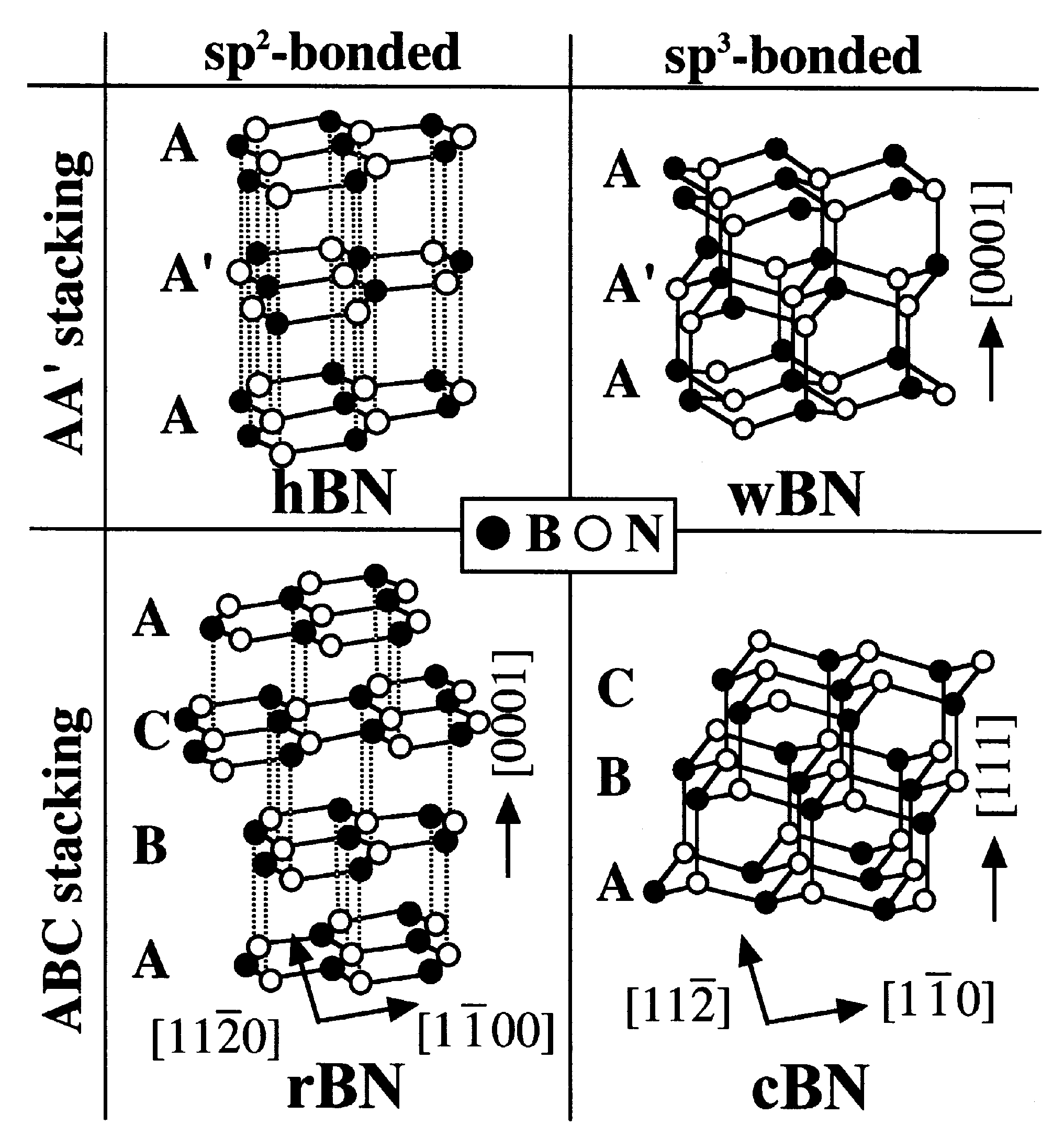
2. Structure of Boron Nitride
3. Synthesis of h-BN via CVD
3.1. B/N Precursors in CVD Synthesis of h-BN

| Precursors | Physical State | Tdec (°C) | Byproduct | Safety | Technique | ||
|---|---|---|---|---|---|---|---|
| Single Reactant | Ammonia borane (AB, NH3-BH3) | Solid | 67 [36] | - | - | LPCVD, APCVD, PECVD | |
| Borazine (B3N3H6) | Liquid | 375 [37] | - | Flammable, toxic | MOCVD, PECVD | ||
| Dual Reactants | Diborane (B2H6) | NH3 * | Gas | 200 [38] | - | Flammable, toxic | MOCVD, LPCVD |
| Trimethylboron (TMB, B(CH3)3) | NH3 * | Gas | 300 [39] | Carbon impurities | Flammable, toxic | MOCVD, LPCVD | |
| Triethylboron (TEB, (B(CH3CH2)3) | NH3 * | Liquid | 400 [39] | Carbon impurities | Flammable, toxic | MOCVD, LPCVD | |
| Trimethoxy borate (TMOB, B(OCH3)3) | N2 * | Liquid | 700 [40] | Carbon impurities | Flammable, toxic | PECVD | |
| Dimethylamine-borane (DMAB, BH3NH(CH3)2) | N2 * | Solid | 120 [41] | Carbon impurities | Flammable, toxic | PECVD | |
| Boron trichloride (BCl3) | NH3 *, N2 * | Gas | 477 [42] | HCl | Highly corrosive | LPCVD, PECVD | |
| Boron trioxide (B2O3) | Ammonium carbonate, ((NH4)2CO3) | Solid | B2O3: 650 [43] (NH4)2CO3: 60 [62] | - | - | APCVD | |
3.2. h-BN Growth via MOCVD
| Precursor | Substrate | Growth Temperature (°C) | Raman FWMH (cm−1) | Thickness (nm) | Deposition Rate (nm/min) | Structure | Year |
|---|---|---|---|---|---|---|---|
| B2H6, NH3 | Si, Ta, Fused Si | 600–800 | - | 100–600 | 5–100 | Below 800 °C: a-BN | 1968 [44] |
| 800 °C: mixture of h-BN and a-BN | |||||||
| Sapphire | 1300 | 24.5 | 3.2 | 0.32 | h-BN film | 2021 [64] | |
| 1160–1400 | - | 41–123 | 0.6–2.1 | Mixture of h-BN and t-BN | 2023 [65] | ||
| B2H6, NH3 or TMB, NH3 | Sapphire | 1360 | B2H6: 21.8 | B2H6: 80 | B2H6: 3.6 | B2H6: h-BN film | 2020 [63] |
| TMB: 42.7 | TMB: 40 | TMB: 1.6 | TMB: t-BN film | ||||
| TEB, NH3 | Sapphire | 950–1000 | - | - | 16 | h-BN film | 1986 [46] |
| 1080 | - | 300 | V/III ratio of 1280: 0.5 | V/III ratio of 1280: h-BN film | 2008 [66] | ||
| V/III of ratio 210: 2 | V/III of ratio 210: t-BN film | ||||||
| 1050 | 26–30 | V/III ratio of 3100: 1.6 | 0.05 | h-BN film | 2014 [67] | ||
| V/III ratio of 450: 17 | |||||||
| 950–1100 | 25–32 | 1.6 | 0.3 | 2016 [68] | |||
| 1100 | 25–30 | 1.5 | - | 2016 [69] | |||
| 1280 | 45 | 3–60 | 0.25 | 2016 [70] | |||
| 1280 | 33.2 | 1.0 μm–2.5 μm | 0.25 | 2017 [71] | |||
| 1330 | - | 70 | 1.2 | 2017 [72] | |||
| 1350 | 27 | 20 | 0.04 | 2018 [73] | |||
| 1280 | 41 | 30–60 | 0.25 | 2019 [74] | |||
| 1050 | 28.84 | 3.07 | 0.08 | 2019 [75] | |||
| (Post-annealed at 1700) | |||||||
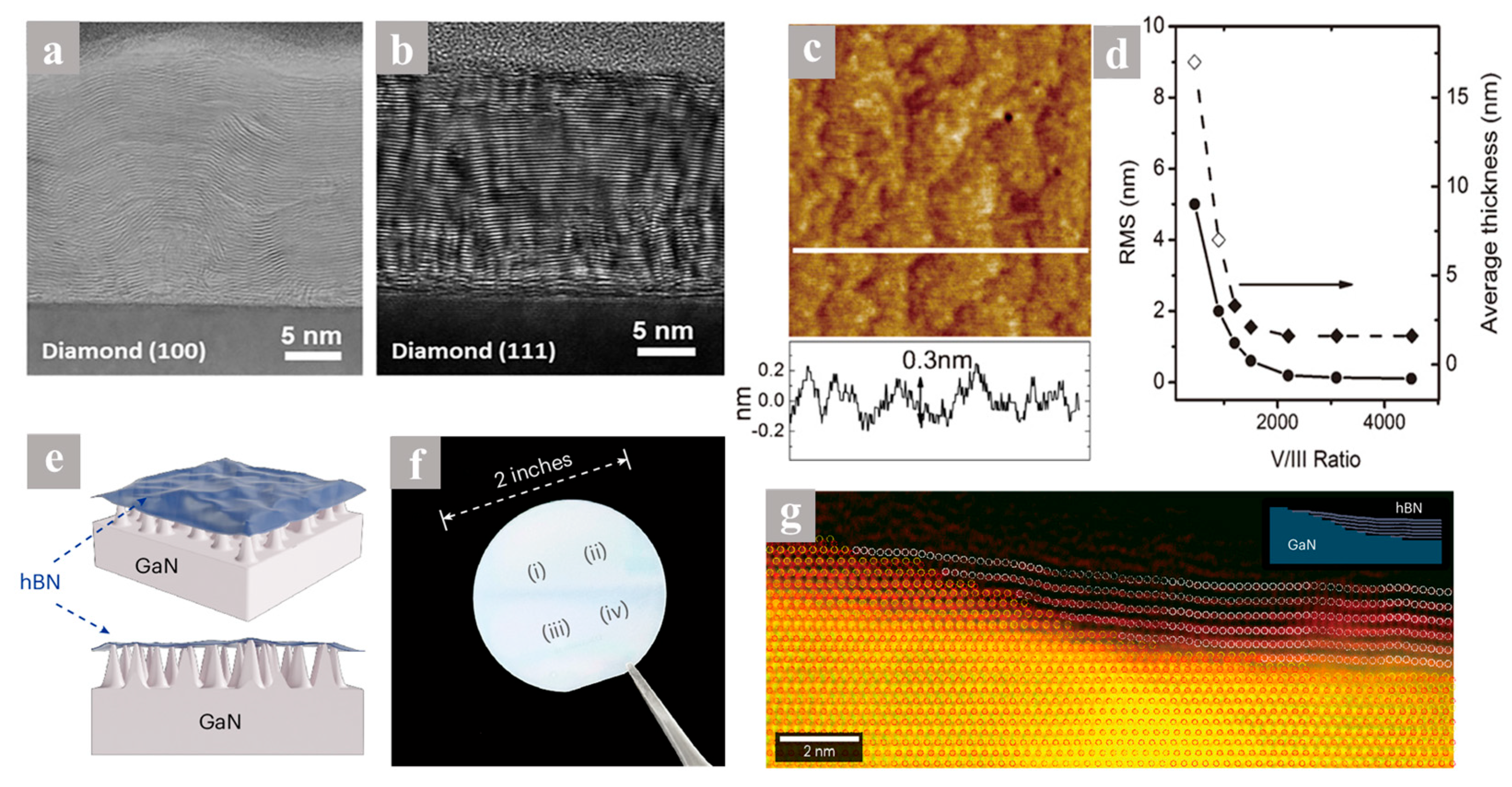
| Diamond (100), (111) | 1380 | - | 7.4 | - | Single crystalline h-BN film | 2020 [76] | |
| Sapphire (1° off-cut) | 1280–1300 | 29.5 | 21 | 0.35 | Mixture of h-BN and t-BN | 2023 [77] | |
| AlN buffer layer/Sapphire | 1300 | - | 1 μm | - | h-BN film | 2011 [79] | |
| BN buffer layer/6H-SiC | 1300 | - | 500 | - | Single crystalline h-BN film | 2013 [78] | |
| AlN buffer layer/Sapphire | 1380 | - | 40 | 25 | h-BN [(0001] || AlN [0001] | 2020 [80] | |
| h-BN [(100] || AlN [110] | |||||||
| GaN buffer layer/Sapphire | 1050 | - | 2.5 | 0.06 | AA stacking h-BN Single crystallinel film | 2025 [81] | |
| TEB, NH3, biscyclopentadienyl-magnesium | AlN buffer layer/Sapphire | 1300 | - | - | - | Mg-doped h-BN film | 2011 [84] |
| TMB, NH3 | Sapphire | 1400 | - | 50 μm | - | Single crystalline h-BN film | 2018 [47] |
| Borazine | Sapphire | 1500 | 29.5 | 30 | 0.17 | Single crystalline h-BN film | 2021 [54] |
3.3. h-BN Growth via LPCVD
| Precursors | Substrates | Tdec (°C) | Growth Temperature (°C) | Raman FWMH (cm−1) | Thickness (nm) | Deposition Rate (nm/min) | Structure | Year | |
|---|---|---|---|---|---|---|---|---|---|
| LPCVD | TEB, NH3 | Si (100) | - | 850–1100 | - | - | t-BN film | 1998 [86] | |
| Sapphire, AlN buffer layer/Sapphire | - | 1500 | 31 | 400 | 1.67 | Sapphire: t-BN AlN/Sapphire: r-BN | 2011 [87] | ||
| AlN buffer layer/Sapphire, 6H-SiC | - | AlN/Sapphire: 1200–1500 6H-SiC: 1600 | - | - | 0.33 | AlN/Sapphire: h-BN at 1200 °C r-BN at 1500 °C 6H-SiC: r-BN at 1600 °C | 2015 [88] | ||
| Amorphous AlNxO1−x buffer layer/Sapphire | - | 1350 | 25 | 300 | 7.5 | TN: Buffer layer nitridation temperature Lower TN: h-BN film Higher TN: t-BN film | 2016 [89] | ||
| Si (111) | - | 1350 | 25 | 1.6 μm | 27 | h-BN film | 2016 [90] | ||
| TEB, NH3/TMB, NH3 | AlN buffer layer/Sapphire (0001), (110), (102), (100) | - | TMB: 1400 TEB: 1500 | - | TMB: 150–1000 nm TEB: 300 nm | 2.5 | r-BN [(110] || AlN [(110]|| Al2O3 [0001] r-BN [(110] || AlN [102]|| Al2O3 [0010] a-BN || Al2O3 (102) a-BN ||Al2O3 (100) | 2022 [91] | |
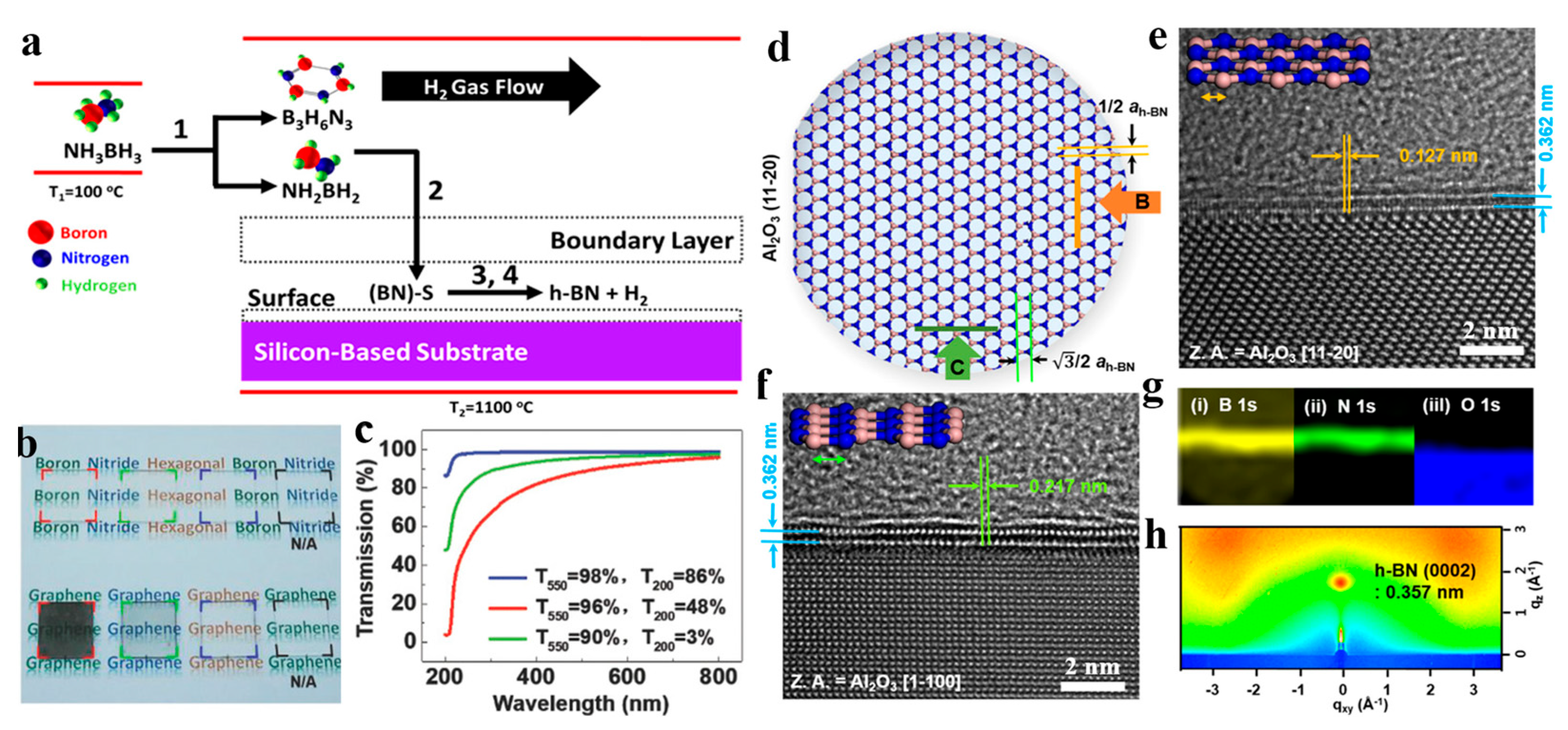
| AB | Si (111) Sapphire | 135 | 1000 | - | 25 | 2.5 | h-BN film | 2014 [55] | |
| Quartz, Si | 100 | 1100 | - | 7 | - | 2015 [92] | |||
| Quartz, SiO2/Si | 100 | 1000 | 42–46 | 2–25 | 0.4–0.8 | 2015 [93] | |||
| Si, Si3N4, SiO2 | 100 | 700–1100 | - | 5 | 0.1 | 2017 [94] | |||
| Sapphire, SiO2 | 75–90 | 1100 | - | monolayer~20 layers | - | 2018 [95] | |||
| Sapphire | 130 | 1400 | - | - | - | Single crystalline AA’ h-BN film | 2016 [97] | ||
| Sapphire | 115 | 1400 | 37.94–39.24 | - | - | High crystalline h-BN film | 2023 [96] | ||
| Sapphire (110) | 115 | 1400 | <30 | 3–35 | 0.58 | [1100]h-BN//Al2O3[110] | 2024 [98] | ||
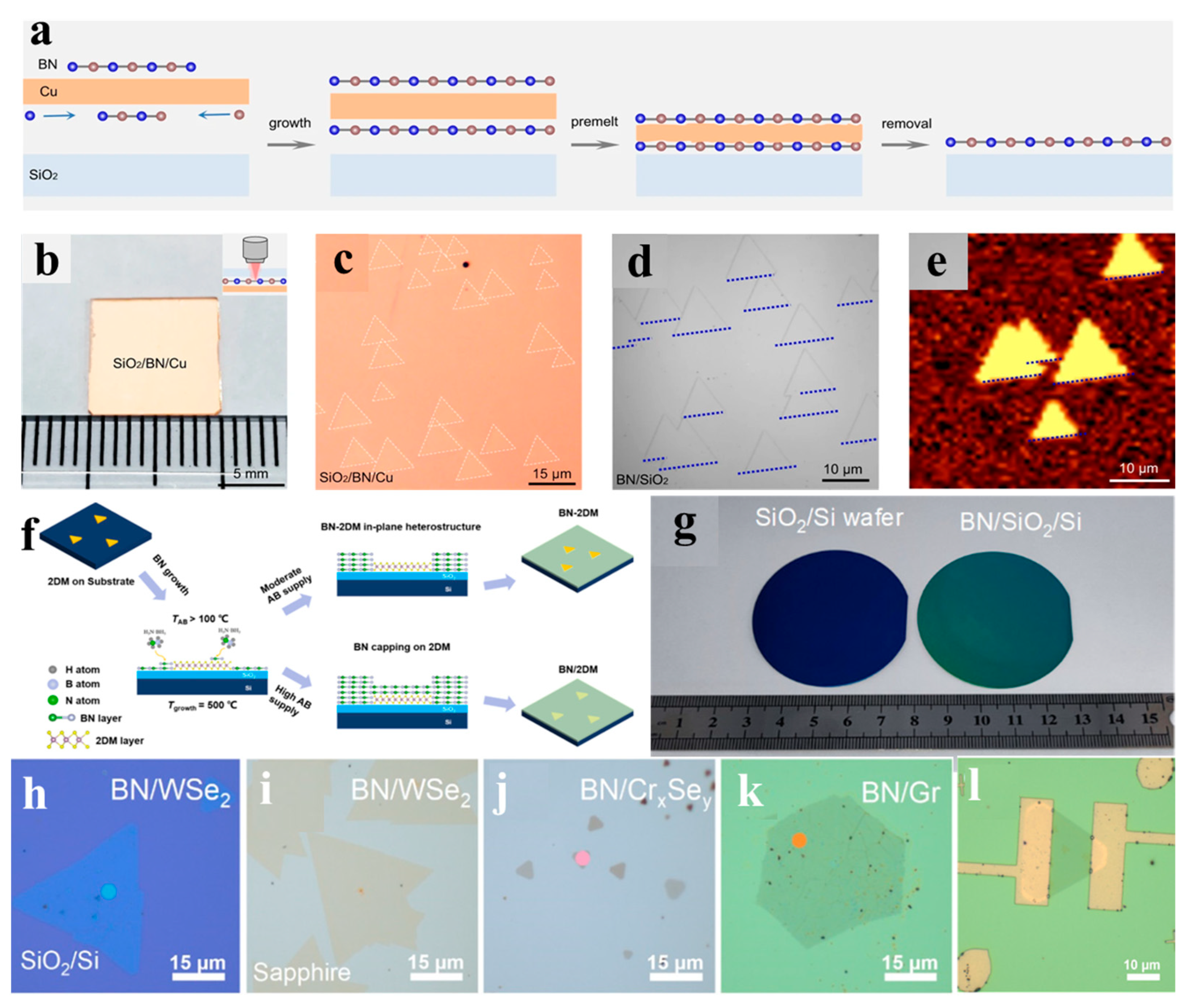
| SiO2, Sapphire, Mica, MoS2, WSe2, CrxSey, Graphene | 110 | 500 | - | 4–31 | 0.2 | a-BN film | 2022 [104] | ||
| Graphene/Ge, SiO2/Si | 100 | 250 | - | 20.4 | - | a-BN film | 2023 [105] | ||
| Cu/SiO2, Cu/SrTiO3, Cu/Sapphire, Cu/Quartz | 85 | 1080 | 13.6 | monolayer | 0.15 | Single crystalline h-BN film | 2023 [100] | ||
| B2H6, NH3 | Sapphire | - | 1100–1300 | 24.6 | 3 | 0.05 | h-BN film | 2021 [51] | |
| BCl3, NH3 | Sapphire | - | 1000–1400 | - | 0.8 μm | 10.83 | h-BN film | 2016 [101] | |
| - | 1200 | - | 1.3 μm | 10.83 | 2021 [102] | ||||
| Si (100) | - | 900–1300 | 60–30 | 2.3 μm | 38.33 | 2021 [103] | |||
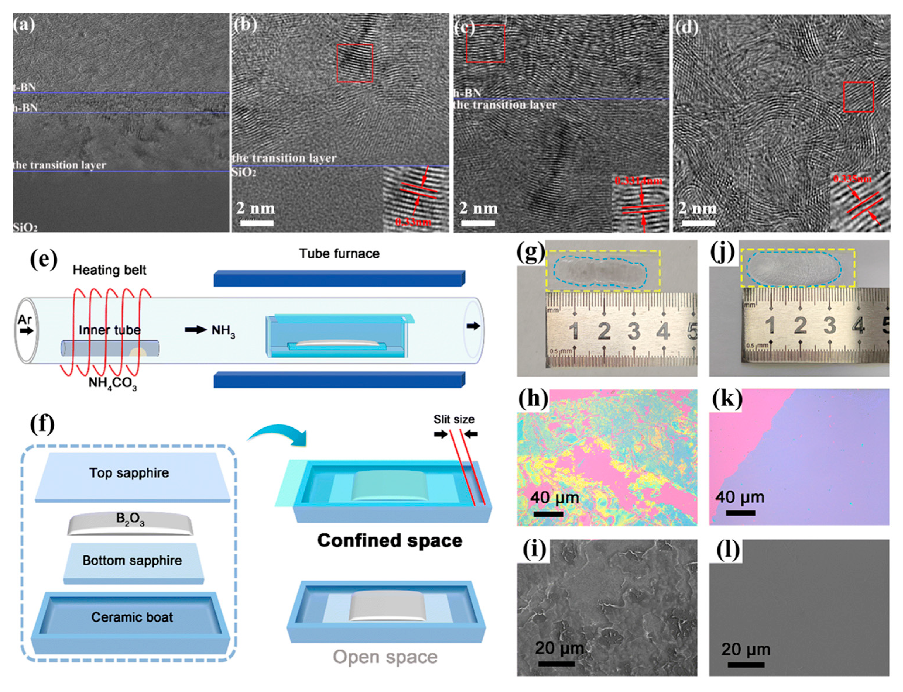
| APCVD | AB | SiO2/Si | 90 | 1360 | 25 | 50–160 | 1.17 | t-BN||h-BN||transition layer|SiO2/Si | 2023 [107] |
| B2O3, (NH4)2CO3 | Sapphire | B2O3: 450 (NH4)2CO3: 60 | 1000–1050 | 23.2 | 5.67–22.82 | 0.32 | h-BN film | 2025 [52] |
3.4. h-BN Growth via APCVD
3.5. h-BN Growth via PECVD
| Technique | B Precursor | N Precursor | Substrate | Growth Temperature (°C) | Thickness (nm) | Deposition Rate (nm/min) | Structure | Year |
|---|---|---|---|---|---|---|---|---|
| RF-PECVD | B2H6 | N2 | Polysilicon | 200–500 | 30–120 | 3 | Mixture of h-BN, c-BN and a-BN | 1997 [108] |
| RF-PECVD | c-Si | 400 | - | 0.05–2 | Mixture of h-BN, c-BN and a-BN | 2000 [109] | ||
| RF-PECVD | c-Si | 180, 340 | - | 0.1–2 | Mixture of h-BN and a-BN | 2002 [110] | ||
| MPCVD | TMOB | N2 | Si (100) | 650–800 | 800 °C: 300 | 2.5 | h-BN film | 2001 [48] |
| MPCVD | DMAB | N2 | Galss-ITO | 350 | - | - | h-BN film | 2001 [49] |
| PECVD | - | Si, Quartz | 280–550 | 0.1 μm–1 μm | - | Mixture of h-BN and c-BN | 2005 [41] | |
| RF-PECVD | Borazine | NH3 | Si (100) | 100–700 | 30–400 | 10–22 | 100–200 °C: a-BN film 300–700 °C: h-BN nanowalls | 2015 [112] |
| ICP-CVD | - | Si | 400 | 3 | 0.03 | a-BN | 2020 [113] | |
| ICP-CVD | N2 | Si, Quartz | 500 | 10 | 1.8 | h-BN film | 2023 [114] | |
| MPCVD | AB | - | Si | 500 | 12 | 4 | h-BN film | 2019 [115] |
| RF-PECVD | - | Sapphire, Si, Quartz, SiO2/Si | 300–500 | 0.85–2.1 | 0.03 | h-BN film | 2019 [116] |
4. Summary and Future Perspectives
Funding
Data Availability Statement
Conflicts of Interest
References
- Ma, K.Y.; Kim, M.; Shin, H.S. Large-Area Hexagonal Boron Nitride Layers by Chemical Vapor Deposition: Growth and Applications for Substrates, Encapsulation, and Membranes. Acc. Mater. Res. 2022, 3, 748–760. [Google Scholar] [CrossRef]
- Roy, S.; Zhang, X.; Puthirath, A.B.; Meiyazhagan, A.; Bhattacharyya, S.; Rahman, M.M.; Babu, G.; Susarla, S.; Saju, S.K.; Tran, M.K.; et al. Structure, Properties and Applications of Two-Dimensional Hexagonal Boron Nitride. Adv. Mater. 2021, 33, e2101589. [Google Scholar] [CrossRef]
- Naclerio, A.E.; Kidambi, P.R. A Review of Scalable Hexagonal Boron Nitride (h-BN) Synthesis for Present and Future Applications. Adv. Mater. 2023, 35, e2207374. [Google Scholar] [CrossRef] [PubMed]
- Wang, Y.; Zhao, C.; Gao, X.; Zheng, L.; Qian, J.; Gao, X.; Li, J.; Tang, J.; Tan, C.; Wang, J.; et al. Ultraflat single-crystal hexagonal boron nitride for wafer-scale integration of a 2D-compatible high-κ metal gate. Nat. Mater. 2024, 23, 1495–1501. [Google Scholar] [CrossRef]
- Cassabois, G.; Valvin, P.; Gil, B. Hexagonal boron nitride is an indirect bandgap semiconductor. Nat. Photonics 2016, 10, 262–266. [Google Scholar] [CrossRef]
- Wang, J.; Xu, T.; Wang, W.; Zhang, Z. Miracle in “white”: Hexagonal boron nitride. Small 2024, 2400489. [Google Scholar] [CrossRef]
- Jiang, H.X.; Lin, J.Y. Hexagonal boron nitride for deep ultraviolet photonic devices. Semicond. Sci. Technol. 2014, 29, 084003. [Google Scholar] [CrossRef]
- Chen, R.; Li, Q.; Fang, W.; Zhang, Q.; Li, J.; Zhang, Z.; Liu, K.; Yun, F.; Guo, Y.; Wang, T.; et al. Deep-UV Light-Emitting Based on the hBN:S/hBN: Mg Homojunction. Adv. Sci. 2025, 12, 2414353. [Google Scholar] [CrossRef] [PubMed]
- Ying, H.; Moore, A.; Cui, J.; Liu, Y.; Li, D.; Han, S.; Yao, Y.; Wang, Z.; Wang, L.; Chen, S. Tailoring the thermal transport properties of monolayer hexagonal boron nitride by grain size engineering. 2D Mater. 2019, 7, 015031. [Google Scholar] [CrossRef]
- Knobloch, T.; Illarionov, Y.Y.; Ducry, F.; Schleich, C.; Wachter, S.; Watanabe, K.; Taniguchi, T.; Mueller, T.; Waltl, M.; Lanza, M.; et al. The performance limits of hexagonal boron nitride as an insulator for scaled CMOS devices based on two-dimensional materials. Nat. Electron. 2021, 4, 98–108. [Google Scholar] [CrossRef]
- Shen, L.; Zhao, Y.; Wang, Y.; Song, R.; Yao, Q.; Chen, S.; Chai, Y. A long-term corrosion barrier with an insulating boron nitride monolayer. J. Mater. Chem. A 2016, 4, 5044–5050. [Google Scholar] [CrossRef]
- Wang, L.; Xu, X.; Zhang, L.; Qiao, R.; Wu, M.; Wang, Z.; Zhang, S.; Liang, J.; Zhang, Z.; Zhang, Z.; et al. Epitaxial growth of a 100-square-centimetre single-crystal hexagonal boron nitride monolayer on copper. Nature 2019, 570, 91–95. [Google Scholar] [CrossRef]
- Chen, T.A.; Chuu, C.P.; Tseng, C.C.; Wen, C.K.; Wong, H.P.; Pan, S.; Li, R.; Chao, T.A.; Chueh, W.C.; Zhang, Y.; et al. Wafer-scale single-crystal hexagonal boron nitride monolayers on Cu (111). Nature 2020, 579, 219–223. [Google Scholar] [CrossRef] [PubMed]
- Ma, K.Y.; Zhang, L.; Jin, S.; Wang, Y.; Yoon, S.I.; Hwang, H.; Oh, J.; Jeong, D.S.; Wang, M.; Chatterjee, S.; et al. Epitaxial single-crystal hexagonal boron nitride multilayers on Ni (111). Nature 2022, 606, 88–93. [Google Scholar] [CrossRef] [PubMed]
- Liu, Z.; Gong, Y.; Zhou, W.; Ma, L.; Yu, J.; Idrobo, J.C.; Jung, J.; MacDonald, A.H.; Vajtai, R.; Lou, J.; et al. Ultrathin high-temperature oxidation-resistant coatings of hexagonal boron nitride. Nat. Commun. 2013, 4, 2541. [Google Scholar] [CrossRef]
- Park, J.H.; Park, J.C.; Yun, S.J.; Kim, H.; Luong, D.H.; Kim, S.M.; Choi, S.H.; Yang, W.; Kong, J.; Kim, K.K.; et al. Large-area monolayer hexagonal boron nitride on Pt foil. ACS Nano 2014, 8, 8520–8528. [Google Scholar] [CrossRef]
- Ying, H.; Li, X.; Li, D.; Huang, M.; Wan, W.; Yao, Q.; Chen, X.; Wang, Z.; Wu, Y.; Wang, L.; et al. Ni foam assisted synthesis of high quality hexagonal boron nitride with large domain size and controllable thickness. 2D Mater. 2018, 5, 025020. [Google Scholar] [CrossRef]
- Li, Y.; Wen, X.; Tan, C.; Li, N.; Li, R.; Huang, X.; Tian, H.; Yao, Z.; Liao, P.; Yu, S.; et al. Synthesis of centimeter-scale high-quality polycrystalline hexagonal boron nitride films from Fe fluxes. Nanoscale 2021, 13, 11223–11231. [Google Scholar] [CrossRef]
- Li, J.; Wang, J.; Zhang, X.; Elias, C.; Ye, G.; Evans, D.; Eda, G.; Redwing, J.M.; Cassabois, G.; Gil, B.; et al. Hexagonal Boron Nitride Crystal Growth from Iron, a Single Component Flux. ACS Nano 2021, 15, 7032–7039. [Google Scholar] [CrossRef]
- Lu, G.; Wu, T.; Yuan, Q.; Wang, H.; Wang, H.; Ding, F.; Xie, X.; Jiang, M. Synthesis of large single-crystal hexagonal boron nitride grains on Cu-Ni alloy. Nat. Commun. 2015, 6, 6160. [Google Scholar] [CrossRef]
- Fukamachi, S.; Solís-Fernández, P.; Kawahara, K.; Tanaka, D.; Otake, T.; Lin, Y.-C.; Suenaga, K.; Ago, H. Large-area synthesis and transfer of multilayer hexagonal boron nitride for enhanced graphene device arrays. Nat. Electron. 2023, 6, 126–136. [Google Scholar] [CrossRef]
- Li, X.; Li, Z.; Qi, L.; Long, Y.; Li, B.; Li, J.; Zhou, J.; Shi, Y.; Yin, J.; Guo, W. A clean dry transfer of hexagonal boron nitride with improved oxidation resistance. Sci. China Mater. 2022, 66, 327–334. [Google Scholar] [CrossRef]
- Li, Q.; Wang, M.; Bai, Y.; Zhang, Q.; Zhang, H.; Tian, Z.; Guo, Y.; Zhu, J.; Liu, Y.; Yun, F.; et al. Two-Inch Wafer-Scale Exfoliation of Hexagonal Boron Nitride Films Fabricated by RF-Sputtering. Adv. Funct. Mater. 2022, 32, 2206094. [Google Scholar] [CrossRef]
- Petrescu, M.; Balint, M.-G. Structure and properties modifications in boron nitride. Part I: Direct polymorphic transformations mechanisms. UPB Sci. Bull. Ser. B 2007, 69, 35–42. [Google Scholar]
- Koga, H.; Nakamura, Y.; Watanabe, M.; Yoshida, T. Molecular dynamics study of deposition mechanism of cubic boron nitride. Sci. Technol. Adv. Mater. 2001, 2, 349–356. [Google Scholar] [CrossRef]
- Qi, J.; Ma, C.; Guo, Q.; Ma, C.; Zhang, Z.; Liu, F.; Shi, X.; Wang, L.; Xue, M.; Wu, M.; et al. Stacking-Controlled Growth of rBN Crystalline Films with High Nonlinear Optical Conversion Efficiency up to 1%. Adv. Mater. 2024, 36, 2303122. [Google Scholar] [CrossRef]
- Mirkarimi, P.B.; McCarty, K.F.; Medlin, D.L. Review of advances in cubic boron nitride film synthesis. Mater. Sci. Eng. R Rep. 1997, 21, 47–100. [Google Scholar] [CrossRef]
- Wills, R.R. Wurtzitic boron nitride—A review. Int. J. High Technol. Ceram. 1985, 1, 139–153. [Google Scholar] [CrossRef]
- Chen, C.; Yin, D.; Kato, T.; Taniguchi, T.; Watanabe, K.; Ma, X.; Ye, H.; Ikuhara, Y. Stabilizing the metastable superhard material wurtzite boron nitride by three-dimensional networks of planar defects. Proc. Natl. Acad. Sci. USA 2019, 116, 11181–11186. [Google Scholar] [CrossRef]
- Liu, C.; Liu, T.; Zhang, Z.; Sun, Z.; Zhang, G.; Wang, E.; Liu, K. Understanding epitaxial growth of two-dimensional materials and their homostructures. Nat. Nanotechnol. 2024, 19, 907–918. [Google Scholar] [CrossRef]
- Zhang, L.; Dong, J.; Ding, F. Strategies, Status, and Challenges in Wafer Scale Single Crystalline Two-Dimensional Materials Synthesis. Chem. Rev. 2021, 121, 6321–6372. [Google Scholar] [CrossRef] [PubMed]
- Kim, G.; Jang, A.R.; Jeong, H.Y.; Lee, Z.; Kang, D.J.; Shin, H.S. Growth of high-crystalline, single-layer hexagonal boron nitride on recyclable platinum foil. Nano Lett. 2013, 13, 1834–1839. [Google Scholar] [CrossRef]
- Jiang, R.; Shi, Z.; Zhao, W.; Gao, B.; Wu, T.; Yuan, Q. Vacancy-Assisted Growth Mechanism of Multilayer Hexagonal Boron Nitride on a Fe(2)B Substrate. J. Phys. Chem. Lett. 2020, 11, 8511–8517. [Google Scholar] [CrossRef] [PubMed]
- Uchida, Y.; Nakandakari, S.; Kawahara, K.; Yamasaki, S.; Mitsuhara, M.; Ago, H. Controlled Growth of Large-Area Uniform Multilayer Hexagonal Boron Nitride as an Effective 2D Substrate. ACS Nano 2018, 12, 6236–6244. [Google Scholar] [CrossRef]
- Yang, Y.; Peng, Y.; Saleem, M.F.; Chen, Z.; Sun, W. Hexagonal Boron Nitride on III-V Compounds: A Review of the Synthesis and Applications. Materials 2022, 15, 4396. [Google Scholar] [CrossRef] [PubMed]
- Baitalow, F.; Baumann, J.; Wolf, G.; Jaenicke-Rößler, K.; Leitner, G. Thermal decomposition of B–N–H compounds investigated by using combined thermoanalytical methods. Thermochim. Acta 2002, 391, 159–168. [Google Scholar] [CrossRef]
- Chiavarino, B.; Crestoni, M.E.; Marzio, A.D.; Fornarini, S.; Rosi, M. Gas-Phase Ion Chemistry of Borazine, an Inorganic Analogue of Benzene. J. Am. Chem. Soc. 1999, 121, 11204–11210. [Google Scholar] [CrossRef]
- Stock, A.; Pohland, E. Borwasserstoffe, IX.: B3N3H6. Berichte Dtsch. Chem. Ges. (A B Ser.) 1926, 59, 2215–2223. [Google Scholar] [CrossRef]
- Brown, M.P.; Holliday, A.K.; Way, G.M.; Whittle, R.B.; Woodard, C.M. Pyrolysis of trimethylborane. Part 2. Formation of carbaboranes and other boron-containing compounds. J. Chem. Soc. Dalton Trans. 1977, 148, 1862–1866. [Google Scholar] [CrossRef]
- Nakamura, K. Preparation of boron nitride thin films by chemical vapor deposition. In Materials Science Forum; Trans Tech Publications Ltd.: Wollerau, Switzerland, 1990; pp. 111–140. [Google Scholar]
- Battiston, G.A.; Berto, D.; Convertino, A.; Emiliani, D.; Figueras, A.; Gerbasi, R.; Viticoli, S. PECVD of h-BN and c-BN films from boranedimethylamine as a single source precursor. Electrochim. Acta 2005, 50, 4600–4604. [Google Scholar] [CrossRef]
- Reinisch, G.; Leyssale, J.M.; Bertrand, N.; Chollon, G.; Langlais, F.; Vignoles, G. Experimental and theoretical investigation of BCl3 decomposition in H2. Surf. Coat. Technol. 2008, 203, 643–647. [Google Scholar] [CrossRef]
- Korobtsov, V.; Balashev, V.; Bazarsad, K. B2O3 decomposition on the Si (100) surface. Phys. Low-Dimens. Struct. 2006, 2, 34–41. [Google Scholar]
- Rand, M.J.; Roberts, J.F. Preparation and Properties of Thin Film Boron Nitride. J. Electrochem. Soc. 1968, 115, 423. [Google Scholar] [CrossRef]
- Long, L.H. Recent Studies of Diborane. In Progress in Inorganic Chemistry; Wiley: Hoboken, NJ, USA, 1972; pp. 1–99. [Google Scholar] [CrossRef]
- Nakamura, K. Preparation and Properties of Boron Nitride Films by Metal Organic Chemical Vapor Deposition. J. Electrochem. Soc. 1986, 133, 1120–1123. [Google Scholar] [CrossRef]
- Maity, A.; Grenadier, S.J.; Li, J.; Lin, J.Y.; Jiang, H.X. Hexagonal boron nitride neutron detectors with high detection efficiencies. J. Appl. Phys. 2018, 123, 044501. [Google Scholar] [CrossRef]
- Thamm, T.; Baumann, W.; Dietrich, D.; Meyer, N.; Stöckel, S.; Marx, G. Preparation of boron nitride thin films by microwave PECVD and their analytical characterisation. Phys. Chem. Chem. Phys. 2001, 3, 5150–5153. [Google Scholar] [CrossRef]
- El-Yadouni, A.; Soltani, A.; Boudrioua, A.; Thevenin, P.; Bath, A.; Loulergue, J.C. Investigation of the optical and electro-optical properties of hexagonal boron nitride thin films deposited by PECVD technique. Opt. Mater. 2001, 17, 319–322. [Google Scholar] [CrossRef]
- Nappini, S.; Píš, I.; Carraro, G.; Celasco, E.; Smerieri, M.; Savio, L.; Magnano, E.; Bondino, F. On-surface synthesis of different boron–nitrogen–carbon heterostructures from dimethylamine borane. Carbon 2017, 120, 185–193. [Google Scholar] [CrossRef]
- Bansal, A.; Zhang, X.; Redwing, J.M. Gas source chemical vapor deposition of hexagonal boron nitride on C-plane sapphire using B2H6 and NH3. J. Mater. Res. 2021, 36, 4678–4687. [Google Scholar] [CrossRef]
- Zhao, Y.; Shi, L.; Li, Y.; Ma, Q.; Huang, J.; Li, W.; Fu, Z.; Wang, H. Facile controlled growth of multilayer h-BN thin films using spaced-confined APCVD and its gate dielectric application. CrystEngComm 2025, 27, 833–842. [Google Scholar] [CrossRef]
- Dai, J.; Wang, Y.; Xu, Z.; Mu, R.; He, L. Influence of hydrogen on growth and microstructure of boron nitride coatings obtained from BCl3–NH3–H2 system by chemical vapor infiltration. Ceram. Int. 2020, 46, 13073–13081. [Google Scholar] [CrossRef]
- Saha, S.; Rice, A.; Ghosh, A.; Hasan, S.M.N.; You, W.; Ma, T.; Hunter, A.; Bissell, L.J.; Bedford, R.; Crawford, M.; et al. Comprehensive characterization and analysis of hexagonal boron nitride on sapphire. AIP Adv. 2021, 11, 055008. [Google Scholar] [CrossRef]
- Bresnehan, M.S.; Hollander, M.J.; Wetherington, M.; Wang, K.; Miyagi, T.; Pastir, G.; Snyder, D.W.; Gengler, J.J.; Voevodin, A.A.; Mitchel, W.C.; et al. Prospects of direct growth boron nitride films as substrates for graphene electronics. J. Mater. Res. 2013, 29, 459–471. [Google Scholar] [CrossRef]
- Rye, R.R.; Tallant, D.R.; Borek, T.T.; Lindquist, D.A.; Paine, R.T. Mechanistic studies of the conversion of borazine polymers to boron nitride. Chem. Mater. 2002, 3, 286–293. [Google Scholar] [CrossRef]
- Shore, S.G.; Parry, R.W. The Crystalline Compound Ammonia-Borane,1 H3nbh3. J. Am. Chem. Soc. 2002, 77, 6084–6085. [Google Scholar] [CrossRef]
- Bowden, M.E.; Gainsford, G.J.; Robinson, W.T. Room-Temperature Structure of Ammonia Borane. Aust. J. Chem. 2007, 60, 149–153. [Google Scholar] [CrossRef]
- Hu, M.G.; Geanangel, R.A.; Wendlandt, W.W. The thermal decomposition of ammonia borane. Thermochim. Acta 1978, 23, 249–255. [Google Scholar] [CrossRef]
- Hinshelwood, C.N.; Burk, R.E. CLIII.—The thermal decomposition of ammonia upon various surfaces. J. Chem. Soc. Trans. 1925, 127, 1105–1117. [Google Scholar] [CrossRef]
- Greenwood, N.N.; Earnshaw, A. Chapter 6 Boron. In Chemistry of the Elements, 2nd ed.; Butterworth-Heinemann: Oxford, UK, 1997; pp. 139–215. [Google Scholar]
- House, J.E. A TG study of the kinetics of decomposition of ammonium carbonate and ammonium bibarbonate. Thermochim. Acta 1980, 40, 225–233. [Google Scholar] [CrossRef]
- Yamada, H.; Inotsume, S.; Kumagai, N.; Yamada, T.; Shimizu, M. Comparative Study of Boron Precursors for Chemical Vapor-Phase Deposition-Grown Hexagonal Boron Nitride Thin Films. Phys. Status Solidi (A) 2020, 218, 2000241. [Google Scholar] [CrossRef]
- Bansal, A.; Hilse, M.; Huet, B.; Wang, K.; Kozhakhmetov, A.; Kim, J.H.; Bachu, S.; Alem, N.; Collazo, R.; Robinson, J.A.; et al. Substrate Modification during Chemical Vapor Deposition of hBN on Sapphire. ACS Appl. Mater. Interfaces 2021, 13, 54516–54526. [Google Scholar] [CrossRef]
- Yamada, H. Reduction in Residual Impurities in Chemical Vapor Deposition–Grown Hexagonal Boron Nitride Thin Films. Phys. Status Solidi (B) 2023, 260, 2200352. [Google Scholar] [CrossRef]
- Kobayashi, Y.; Akasaka, T. Hexagonal BN epitaxial growth on (0001) sapphire substrate by MOVPE. J. Cryst. Growth 2008, 310, 5044–5047. [Google Scholar] [CrossRef]
- Paduano, Q.S.; Snure, M.; Bondy, J.; Zens, T.W.C. Self-terminating growth in hexagonal boron nitride by metal organic chemical vapor deposition. Appl. Phys. Express 2014, 7, 071004. [Google Scholar] [CrossRef]
- Paduano, Q.; Snure, M. Metal-Organic chemical vapor deposition of BN on sapphire and its heterostructures with 2D and 3D materials. MRS Adv. 2016, 1, 2273–2283. [Google Scholar] [CrossRef]
- Snure, M.; Paduano, Q.; Kiefer, A. Effect of surface nitridation on the epitaxial growth of few-layer sp2 BN. J. Cryst. Growth 2016, 436, 16–22. [Google Scholar] [CrossRef]
- Li, X.; Sundaram, S.; El Gmili, Y.; Ayari, T.; Puybaret, R.; Patriarche, G.; Voss, P.L.; Salvestrini, J.P.; Ougazzaden, A. Large-Area Two-Dimensional Layered Hexagonal Boron Nitride Grown on Sapphire by Metalorganic Vapor Phase Epitaxy. Cryst. Growth Des. 2016, 16, 3409–3415. [Google Scholar] [CrossRef]
- Li, X.; Jordan, M.B.; Ayari, T.; Sundaram, S.; El Gmili, Y.; Alam, S.; Alam, M.; Patriarche, G.; Voss, P.L.; Paul Salvestrini, J.; et al. Flexible metal-semiconductor-metal device prototype on wafer-scale thick boron nitride layers grown by MOVPE. Sci. Rep. 2017, 7, 786. [Google Scholar] [CrossRef]
- Yang, X.; Nitta, S.; Nagamatsu, K.; Bae, S.-Y.; Lee, H.-J.; Liu, Y.; Pristovsek, M.; Honda, Y.; Amano, H. Growth of hexagonal boron nitride on sapphire substrate by pulsed-mode metalorganic vapor phase epitaxy. J. Cryst. Growth 2017, 482, 1–8. [Google Scholar] [CrossRef]
- Chugh, D.; Wong-Leung, J.; Li, L.; Lysevych, M.; Tan, H.H.; Jagadish, C. Flow modulation epitaxy of hexagonal boron nitride. 2D Mater. 2018, 5, 045018. [Google Scholar] [CrossRef]
- Sundaram, S.; Li, X.; Alam, S.; Halfaya, Y.; Patriarche, G.; Ougazzaden, A. Wafer-scale MOVPE growth and characterization of highly ordered h-BN on patterned sapphire substrates. J. Cryst. Growth 2019, 509, 40–43. [Google Scholar] [CrossRef]
- Lee, S.H.; Jeong, H.; Okello, O.F.N.; Xiao, S.; Moon, S.; Kim, D.Y.; Kim, G.Y.; Lo, J.I.; Peng, Y.C.; Cheng, B.M.; et al. Improvements in structural and optical properties of wafer-scale hexagonal boron nitride film by post-growth annealing. Sci. Rep. 2019, 9, 10590. [Google Scholar] [CrossRef] [PubMed]
- Yang, X.; Pristovsek, M.; Nitta, S.; Liu, Y.; Honda, Y.; Koide, Y.; Kawarada, H.; Amano, H. Epitaxial Combination of Two-Dimensional Hexagonal Boron Nitride with Single-Crystalline Diamond Substrate. ACS Appl. Mater. Interfaces 2020, 12, 46466–46475. [Google Scholar] [CrossRef]
- Tokarczyk, M.; Dąbrowska, A.K.; Kowalski, G.; Bożek, R.; Iwański, J.; Binder, J.; Stępniewski, R.; Wysmołek, A. Effective substrate for the growth of multilayer h-BN on sapphire—Substrate off-cut, pre-growth, and post-growth conditions in metal-organic vapor phase epitaxy. 2D Mater. 2023, 10, 025010. [Google Scholar] [CrossRef]
- Majety, S.; Li, J.; Zhao, W.P.; Huang, B.; Wei, S.H.; Lin, J.Y.; Jiang, H.X. Hexagonal boron nitride and 6H-SiC heterostructures. Appl. Phys. Lett. 2013, 102, 213505. [Google Scholar] [CrossRef]
- Li, J.; Dahal, R.; Majety, S.; Lin, J.Y.; Jiang, H.X. Hexagonal boron nitride epitaxial layers as neutron detector materials. Nucl. Instrum. Methods Phys. Res. Sect. A Accel. Spectrometers Detect. Assoc. Equip. 2011, 654, 417–420. [Google Scholar] [CrossRef]
- Yang, X.; Nitta, S.; Pristovsek, M.; Liu, Y.; Liao, Y.; Kushimoto, M.; Honda, Y.; Amano, H. Scalable synthesis of multilayer h-BN on AlN by metalorganic vapor phase epitaxy: Nucleation and growth mechanism. 2D Mater. 2019, 7, 015004. [Google Scholar] [CrossRef]
- Moon, S.; Okello, O.F.N.; Rousseau, A.; Choi, C.-W.; Kim, Y.; Park, Y.; Kim, J.; Kim, J.; Kim, M.; Valvin, P.; et al. Wafer-scale AA-stacked hexagonal boron nitride grown on a GaN substrate. Nat. Mater. 2025, 24, 843–851. [Google Scholar] [CrossRef]
- Steckl, A.J.; Zavada, J.M. Optoelectronic Properties and Applications of Rare-Earth-Doped GaN. MRS Bull. 1999, 24, 33–38. [Google Scholar] [CrossRef]
- Liang, Y.-H.; Towe, E. Progress in efficient doping of high aluminum-containing group III-nitrides. Appl. Phys. Rev. 2018, 5, 011107. [Google Scholar] [CrossRef]
- Dahal, R.; Li, J.; Majety, S.; Pantha, B.N.; Cao, X.K.; Lin, J.Y.; Jiang, H.X. Epitaxially grown semiconducting hexagonal boron nitride as a deep ultraviolet photonic material. Appl. Phys. Lett. 2011, 98, 211110. [Google Scholar] [CrossRef]
- Ullah, Z.; Riaz, S.; Li, Q.; Atiq, S.; Saleem, M.; Azhar, M.; Naseem, S.; Liu, L. A comparative study of graphene growth by APCVD, LPCVD and PECVD. Mater. Res. Express 2018, 5, 035606. [Google Scholar] [CrossRef]
- Jin, Y.-G.; Lee, S.-Y.; Nam, Y.-W.; Lee, J.K.; Park, D. A study of deposition rate and characterization of bn thin films prepared by cvd. Korean J. Chem. Eng. 1998, 15, 652–657. [Google Scholar] [CrossRef]
- Chubarov, M.; Pedersen, H.; Högberg, H.; Darakchieva, V.; Jensen, J.; Persson, P.O.Å.; Henry, A. Epitaxial CVD growth of sp2-hybridized boron nitride using aluminum nitride as buffer layer. Phys. Status Solidi (RRL)–Rapid Res. Lett. 2011, 5, 397–399. [Google Scholar] [CrossRef]
- Chubarov, M.; Pedersen, H.; Högberg, H.; Henry, A.; Czigány, Z. Initial stages of growth and the influence of temperature during chemical vapor deposition of sp2-BN films. J. Vac. Sci. Technol. A Vac. Surf. Film. 2015, 33, 061520. [Google Scholar] [CrossRef]
- Ahmed, K.; Dahal, R.; Weltz, A.; Lu, J.J.Q.; Danon, Y.; Bhat, I.B. Effects of sapphire nitridation and growth temperature on the epitaxial growth of hexagonal boron nitride on sapphire. Mater. Res. Express 2017, 4, 015007. [Google Scholar] [CrossRef]
- Ahmed, K.; Dahal, R.; Weltz, A.; Lu, J.Q.; Danon, Y.; Bhat, I.B. Growth of hexagonal boron nitride on (111) Si for deep UV photonics and thermal neutron detection. Appl. Phys. Lett. 2016, 109, 113501. [Google Scholar] [CrossRef]
- Sharma, S.; Souqui, L.; Pedersen, H.; Högberg, H. Chemical vapor deposition of sp2-boron nitride films on Al2O3 (0001), (112¯), (11¯02), and (101¯) substrates. J. Vac. Sci. Technol. A 2022, 40, 033404. [Google Scholar] [CrossRef]
- Behura, S.; Nguyen, P.; Che, S.; Debbarma, R.; Berry, V. Large-Area, Transfer-Free, Oxide-Assisted Synthesis of Hexagonal Boron Nitride Films and Their Heterostructures with MoS2 and WS2. J. Am. Chem. Soc. 2015, 137, 13060–13065. [Google Scholar] [CrossRef]
- Tay, R.Y.; Tsang, S.H.; Loeblein, M.; Chow, W.L.; Loh, G.C.; Toh, J.W.; Ang, S.L.; Teo, E.H.T. Direct growth of nanocrystalline hexagonal boron nitride films on dielectric substrates. Appl. Phys. Lett. 2015, 106, 101901. [Google Scholar] [CrossRef]
- Behura, S.; Nguyen, P.; Debbarma, R.; Che, S.; Seacrist, M.R.; Berry, V. Chemical Interaction-Guided, Metal-Free Growth of Large-Area Hexagonal Boron Nitride on Silicon-Based Substrates. ACS Nano 2017, 11, 4985–4994. [Google Scholar] [CrossRef] [PubMed]
- Li, Q.; Wu, Q.; Gao, J.; Wei, T.; Sun, J.; Hong, H.; Dou, Z.; Zhang, Z.; Rümmeli, M.H.; Gao, P.; et al. Direct Growth of 5 in. Uniform Hexagonal Boron Nitride on Glass for High-Performance Deep-Ultraviolet Light-Emitting Diodes. Adv. Mater. Interfaces 2018, 5, 1800662. [Google Scholar] [CrossRef]
- Chen, R.; Li, Q.; Zhang, Q.; Li, J.; Zhang, Z.; Fang, W.; Wang, L.; Yun, F.; Wang, T.; Hao, Y. High-Crystallinity and High-Temperature Stability of the Hexagonal Boron Nitride Film Grown on Sapphire. Cryst. Growth Des. 2023, 23, 8783–8792. [Google Scholar] [CrossRef]
- Jang, A.R.; Hong, S.; Hyun, C.; Yoon, S.I.; Kim, G.; Jeong, H.Y.; Shin, T.J.; Park, S.O.; Wong, K.; Kwak, S.K.; et al. Wafer-Scale and Wrinkle-Free Epitaxial Growth of Single-Orientated Multilayer Hexagonal Boron Nitride on Sapphire. Nano Lett. 2016, 16, 3360–3366. [Google Scholar] [CrossRef] [PubMed]
- Chen, R.; Li, Q.; Li, J.; Zhang, Q.; Fang, W.; Liu, K.; Zhang, Z.; Yun, F. Mechanical peeling characteristics of large-scale high-crystallinity hBN films. Appl. Surf. Sci. 2024, 667, 160421. [Google Scholar] [CrossRef]
- Chen, Y.; Liang, H.; Xia, X.; Zhang, H.; Shi, J.; Abbas, Q.; Du, G. Growth temperature impact on film quality of hBN grown on Al2O3 using non-catalyzed borazane CVD. J. Mater. Sci. Mater. Electron. 2017, 28, 14341–14347. [Google Scholar] [CrossRef]
- Zeng, F.; Wang, R.; Wei, W.; Feng, Z.; Guo, Q.; Ren, Y.; Cui, G.; Zou, D.; Zhang, Z.; Liu, S.; et al. Stamped production of single-crystal hexagonal boron nitride monolayers on various insulating substrates. Nat. Commun. 2023, 14, 6421. [Google Scholar] [CrossRef]
- Umehara, N.; Masuda, A.; Shimizu, T.; Kuwahara, I.; Kouno, T.; Kominami, H.; Hara, K. Influences of growth parameters on the film formation of hexagonal boron nitride thin films grown on sapphire substrates by low-pressure chemical vapor deposition. Jpn. J. Appl. Phys. 2016, 55, 05FD09. [Google Scholar] [CrossRef]
- Umehara, N.; Adachi, T.; Masuda, A.; Kouno, T.; Kominami, H.; Hara, K. Room-temperature intrinsic excitonic luminescence from a hexagonal boron nitride thin film grown on a sapphire substrate by low-pressure chemical vapor deposition using BCl3 as a boron source. Jpn. J. Appl. Phys. 2021, 60, 075502. [Google Scholar] [CrossRef]
- Chen, X.; Tan, C.; Liu, X.; Luan, K.; Guan, Y.; Liu, X.; Zhao, J.; Hou, L.; Gao, Y.; Chen, Z. Growth of hexagonal boron nitride films on silicon substrates by low-pressure chemical vapor deposition. J. Mater. Sci. Mater. Electron. 2021, 32, 3713–3719. [Google Scholar] [CrossRef]
- Lu, Z.; Zhu, M.; Liu, Y.; Zhang, G.; Tan, Z.; Li, X.; Xu, S.; Wang, L.; Dou, R.; Wang, B.; et al. Low-Temperature Synthesis of Boron Nitride as a Large-Scale Passivation and Protection Layer for Two-Dimensional Materials and High-Performance Devices. ACS Appl. Mater. Interfaces 2022, 14, 25984–25992. [Google Scholar] [CrossRef] [PubMed]
- Sattari-Esfahlan, S.M.; Kim, H.G.; Hyun, S.H.; Choi, J.H.; Hwang, H.S.; Kim, E.T.; Park, H.G.; Lee, J.H. Low-Temperature Direct Growth of Amorphous Boron Nitride Films for High-Performance Nanoelectronic Device Applications. ACS Appl. Mater. Interfaces 2023, 15, 7274–7281. [Google Scholar] [CrossRef]
- Glavin, N.R.; Muratore, C.; Jespersen, M.L.; Hu, J.; Hagerty, P.T.; Hilton, A.M.; Blake, A.T.; Grabowski, C.A.; Durstock, M.F.; McConney, M.E.; et al. Amorphous Boron Nitride: A Universal, Ultrathin Dielectric For 2D Nanoelectronics. Adv. Funct. Mater. 2016, 26, 2640–2647. [Google Scholar] [CrossRef]
- Yang, Y.; Sun, W. Atmospheric-pressure CVD-grown h-BN for the detector with deep ultraviolet response. Phys. Scr. 2023, 98, 125989. [Google Scholar] [CrossRef]
- Carreño, M.N.P.; Bottecchia, J.P.; Pereyra, I. Low temperature plasma enhanced chemical vapour deposition boron nitride. Thin Solid Films 1997, 308–309, 219–222. [Google Scholar] [CrossRef]
- Vilcarromero, J.; Carreño, M.N.P.; Pereyra, I. Mechanical properties of boron nitride thin films obtained by RF-PECVD at low temperatures. Thin Solid Films 2000, 373, 273–276. [Google Scholar] [CrossRef]
- Vilcarromero, J.; Carreño, M.N.P.; Pereyra, I.; Cruz, N.C.; Rangel, E.C. Preparation and Characterization of Nanocrystalline h-BN Films Prepared by PECVD Method. Braz. J. Phys. 2002, 32, 372–375. [Google Scholar] [CrossRef]
- Chakrabarty, K.; Arnold, I.; Catledge, S.A. Hexagonal boron nitride grown using high atomic boron emission during microwave plasma chemical vapor deposition. J. Vac. Sci. Technol. A Vac. Surf. Film. 2019, 37, 061507. [Google Scholar] [CrossRef]
- Merenkov, I.S.; Kosinova, M.L.; Ermakova, E.N.; Maksimovskii, E.A.; Rumyantsev, Y.M. PECVD synthesis of hexagonal boron nitride nanowalls from a borazine + ammonia mixture. Inorg. Mater. 2015, 51, 1097–1103. [Google Scholar] [CrossRef]
- Hong, S.; Lee, C.S.; Lee, M.H.; Lee, Y.; Ma, K.Y.; Kim, G.; Yoon, S.I.; Ihm, K.; Kim, K.J.; Shin, T.J.; et al. Ultralow-dielectric-constant amorphous boron nitride. Nature 2020, 582, 511–514. [Google Scholar] [CrossRef]
- Yamamoto, M.; Murata, H.; Miyata, N.; Takashima, H.; Nagao, M.; Mimura, H.; Neo, Y.; Murakami, K. Low-Temperature Direct Synthesis of Multilayered h-BN without Catalysts by Inductively Coupled Plasma-Enhanced Chemical Vapor Deposition. ACS Omega 2023, 8, 5497–5505. [Google Scholar] [CrossRef] [PubMed]
- Singh, R.; Kalita, G.; Mahyavanshi, R.D.; Adhikari, S.; Uchida, H.; Tanemura, M.; Umeno, M.; Kawahara, T. Low temperature wafer-scale synthesis of hexagonal boron nitride by microwave assisted surface wave plasma chemical vapour deposition. AIP Adv. 2019, 9, 035043. [Google Scholar] [CrossRef]
- Liu, D.; Chen, X.; Yan, Y.; Zhang, Z.; Jin, Z.; Yi, K.; Zhang, C.; Zheng, Y.; Wang, Y.; Yang, J.; et al. Conformal hexagonal-boron nitride dielectric interface for tungsten diselenide devices with improved mobility and thermal dissipation. Nat. Commun. 2019, 10, 1188. [Google Scholar] [CrossRef] [PubMed]
- Li, J.; Samad, A.; Yuan, Y.; Wang, Q.; Hedhili, M.N.; Lanza, M.; Schwingenschlogl, U.; Abate, I.; Akinwande, D.; Liu, Z.; et al. Single-crystal hBN Monolayers from Aligned Hexagonal Islands. Nat. Commun. 2024, 15, 8589. [Google Scholar] [CrossRef]
- Li, J.; Yuan, Y.; Lanza, M.; Abate, I.; Tian, B.; Zhang, X. Nonepitaxial Wafer-Scale Single-Crystal 2D Materials on Insulators. Adv. Mater. 2024, 36, e2310921. [Google Scholar] [CrossRef]
- Wang, X.; Hooper, T.N.; Kumar, A.; Priest, I.K.; Sheng, Y.; Samuels, T.O.M.; Wang, S.; Robertson, A.W.; Pacios, M.; Bhaskaran, H.; et al. Oligomeric aminoborane precursors for the chemical vapour deposition growth of few-layer hexagonal boron nitride. CrystEngComm 2017, 19, 285–294. [Google Scholar] [CrossRef]

Disclaimer/Publisher’s Note: The statements, opinions and data contained in all publications are solely those of the individual author(s) and contributor(s) and not of MDPI and/or the editor(s). MDPI and/or the editor(s) disclaim responsibility for any injury to people or property resulting from any ideas, methods, instructions or products referred to in the content. |
© 2025 by the authors. Licensee MDPI, Basel, Switzerland. This article is an open access article distributed under the terms and conditions of the Creative Commons Attribution (CC BY) license (https://creativecommons.org/licenses/by/4.0/).
Share and Cite
Xu, H.; Li, K.; Tan, Z.; Jia, J.; Wang, L.; Chen, S. Recent Advances in Chemical Vapor Deposition of Hexagonal Boron Nitride on Insulating Substrates. Nanomaterials 2025, 15, 1059. https://doi.org/10.3390/nano15141059
Xu H, Li K, Tan Z, Jia J, Wang L, Chen S. Recent Advances in Chemical Vapor Deposition of Hexagonal Boron Nitride on Insulating Substrates. Nanomaterials. 2025; 15(14):1059. https://doi.org/10.3390/nano15141059
Chicago/Turabian StyleXu, Hua, Kai Li, Zuoquan Tan, Jiaqi Jia, Le Wang, and Shanshan Chen. 2025. "Recent Advances in Chemical Vapor Deposition of Hexagonal Boron Nitride on Insulating Substrates" Nanomaterials 15, no. 14: 1059. https://doi.org/10.3390/nano15141059
APA StyleXu, H., Li, K., Tan, Z., Jia, J., Wang, L., & Chen, S. (2025). Recent Advances in Chemical Vapor Deposition of Hexagonal Boron Nitride on Insulating Substrates. Nanomaterials, 15(14), 1059. https://doi.org/10.3390/nano15141059