Article

Low Resistivity and High Carrier Concentration in SnO2 Thin Films: The Impact of Nitrogen–Hydrogen Annealing Treatments

1
Xiamen Key Laboratory of Development and Application for Advanced Semiconductor Coating Technology, The School of Opto-Electronic and Communication Engineering, Xiamen University of Technology, Xiamen 361024, China
2
Institute of Optoelectronic Display, National & Local United Engineering Lab of Flat Panel Display Technology, Fuzhou University, Fuzhou 350002, China
3
School of Advanced Manufacturing, Fuzhou University, Quanzhou 362200, China
4
Department of Computer Science and Information Engineering, Asia University, Taichung 413, Taiwan
*
Author to whom correspondence should be addressed.
Nanomaterials 2025, 15(13), 986; https://doi.org/10.3390/nano15130986 (registering DOI)
Submission received: 22 May 2025 / Revised: 24 June 2025 / Accepted: 24 June 2025 / Published: 25 June 2025
(This article belongs to the Special Issue Thin Films for Efficient Perovskite Solar Cells)

Abstract

The tin dioxide (SnO2) thin films in this work were prepared by using plasma-enhanced atomic layer deposition (PEALD), and a systematic analysis was conducted to evaluate the influence of post-deposition annealing at various temperatures in a nitrogen–hydrogen mixed atmosphere on their surface morphology, optical behavior, and electrical performance. The SnO2 films were characterized by using X-ray diffraction (XRD), X-ray photoelectron spectroscopy (XPS), scanning electron microscopy (SEM), transmission electron microscopy (TEM), and Hall effect measurements. With increasing annealing temperatures, the SnO2 films exhibited enhanced crystallinity, a higher oxygen vacancy (OV) peak area ratio, and improved mobility and carrier concentration. These enhancements make the annealed SnO2 films highly suitable as electron transport layers (ETLs) in perovskite solar cells (PSCs), providing practical guidance for the design of high-performance PSCs.
Keywords:
PEALD; SnO2; annealing; ETL; PSCs

Graphical Abstract

1. Introduction

Perovskite solar cells (PSCs) have emerged as a highly promising class of photovoltaic technologies due to their remarkable power conversion efficiencies (PCEs), low fabrication costs, and compatibility with large-area substrates [1,2,3,4,5]. Within the device architecture, the electron transport layer (ETL) plays a pivotal role in facilitating efficient electron extraction, blocking holes, and influencing the overall performance and stability of the device. Tin dioxide (SnO2) is widely regarded as an ideal ETL candidate owing to its high electron mobility, excellent optical transparency, favorable energy band alignment with perovskite absorbers, and good chemical stability [6,7,8,9,10,11]. However, the electrical performance of SnO2 films is highly sensitive to their crystalline quality, oxygen vacancy (OV) concentration, and interface properties, all of which are strongly influenced by deposition technique and post-treatment conditions [12,13,14].
Recent advancements in light management strategies have introduced microstructured or patterned glass substrates in PSC architectures to enhance photon harvesting and reduce optical reflection [15,16,17,18]. These complex topographies demand deposition techniques capable of producing conformal, uniform, and pinhole-free films over uneven surfaces. Conventional deposition methods, such as sputtering or sol–gel processes, often struggle to meet these requirements due to limited step coverage and poor thickness control on textured substrates.
Compared with various physical vapor deposition methods, PEALD combines the advantages of atomic-level thickness control and excellent conformality inherent in ALD processes while enabling low-temperature deposition and broader material versatility through plasma activation [19,20,21,22,23,24]. These advantages make PEALD an ideal method for depositing SnO2 ETLs on microstructured glass substrates used in modern PSCs. However, the electrical and structural properties of PEALD-deposited SnO2 films can be further tuned through post-deposition thermal annealing, especially in a reducing atmosphere such as forming gas (N2/H2), which can modulate oxygen vacancy content and promote crystallization. Despite the promising application of PEALD-derived SnO2 in PSCs, comprehensive investigations into the influence of annealing temperature on the microstructural evolution and functional performance of these films remain limited [25].
In this work, SnO2 thin films were deposited by using PEALD, followed by post-deposition annealing at various temperatures in a N2/H2 (95:5) atmosphere. The influence of thermal treatment on the morphology, crystal structure, chemical composition, and electrical properties of the films was systematically examined through a combination of characterization techniques, including X-ray diffraction (XRD), X-ray photoelectron spectroscopy (XPS), scanning electron microscopy (SEM), transmission electron microscopy (TEM), and Hall effect measurements. The results provide insight into the thermal evolution of SnO2 films and demonstrate their suitability as ETLs for high-efficiency PSCs, especially in architectures employing microstructured glass substrates.

2. Materials and Methods

Silicon wafers and glass acted as substrates for the deposited SnO2 films after ultrasonic treatment with isopropanol ethanol and deionization for 10 min. Glass substrates (Corning® EXG, Corning, NY, USA, 100 mm × 100 mm × 0.2 mm) were used for electrical characterizations. Single-crystal p-type Si wafers (450 μm thickness, 50 Ω·cm) were used for structural characterizations including XRD, XPS, SEM, and TEM. The SnO2 films were deposited by using PEALD (R-200, Picosun, Espoo, Finland) by alternately exposing the sample to Tetrakis(dimethylamino)tin (TDMASn) and O2 plasma, in which TDMASn was employed as the tin precursor, while oxygen plasma served as the oxidant. The TDMASn precursor was maintained at 50 °C in a bubbler to ensure adequate vapor pressure, and high-purity argon (80 sccm) was used as the carrier and purge gas. The substrates were heated to 200 °C during the deposition process. Each ALD cycle consisted of a 1.6 s TDMASn pulse, followed by a 6 s Ar purge. Subsequently, O2 gas (150 sccm) was introduced and excited into plasma at a power of 2500 W, with an 11 s plasma exposure time and a 5 s purge step. A continuous TDMASn carrier gas flow of 120 sccm and a dilution flow of 400 sccm were maintained throughout the process to ensure stable precursor delivery. A total of 308 cycles were used to achieve a film thickness of approximately 41.26 nm. Including all precursor exposure and purge steps, the entire deposition process took around 2 h. The detailed process parameters are summarized in Table 1. SnO2 thin films were annealed at 300, 400, 500, and 600 °C using a vacuum tube furnace (YTGM 310-17, Shanghai Yetuo Technology Co., Shanghai, China). To prevent thermal deformation of the glass substrate, whose softening point is approximately 700 °C, the annealing temperature in this study was restricted to a maximum of 600 °C [26,27,28]. Prior to heating, the furnace tube was evacuated to a base pressure of 1.5 mTorr (0.2 Pa) to minimize contamination. The samples were loaded into alumina (Al2O3) crucibles and subjected to a controlled heating process at a rate of 5 °C/min until the target annealing temperature was reached. They were then maintained at this temperature for 1 hour (isothermal hold), followed by natural cooling to below 100 °C. A forming gas atmosphere (N2/H2 = 95:5) was introduced at the beginning of the heating process and maintained throughout the entire annealing cycle. A chamber pressure of 15 mTorr was sustained during the ramping period and increased to 1.5 Torr during the one-hour annealing stage, while the gas flow rate remained fixed at 3.0 L/min.
The crystalline structure of the SnO2 thin films was characterized via grazing incidence X-ray diffraction (GIXRD; Rigaku TTRAX III, Ibaraki, Japan) using Cu Kα radiation (λ = 0.15418 nm) at a fixed incident angle of 0.5°, which effectively suppresses substrate signals and enhances the diffraction signal from the thin films. The elemental composition and chemical states were analyzed via X-ray photoelectron spectroscopy (XPS; ESCALAB 250Xi, Thermo Fisher Scientific, Waltham, MA, USA). Al Kα radiation (1486.6 eV) was used as the X-ray source, which typically provides an information depth of approximately 5–10 nm, depending on the material and detection angle. To minimize the effect of surface contamination and obtain representative chemical information from the near-surface region, Ar+ ion sputtering was performed for 30 seconds at a rate of ~0.275 nm/s prior to data acquisition, effectively removing approximately 8–9 nm from the film surface. As a result, the obtained XPS spectra reflect the sub-surface composition rather than just the outermost surface, ensuring more reliable chemical state analysis. Electrical properties of the SnO2 thin films, including resistivity, carrier concentration, and mobility, were measured using a Hall effect measurement system (HMS-5000; Ecopia, Anyang, Republic of Korea). Hall measurements were performed in the Van der Pauw configuration at room temperature (~25 °C). To eliminate parasitic conduction, the SnO2 films were deposited on insulating glass substrates. Square-shaped samples with dimensions of approximately 1 cm × 1 cm were prepared, and four small indium contacts were manually pressed onto the corners to ensure good ohmic contact. The surface morphology of the films was examined using field emission scanning electron microscopy (FESEM; Sigma 500, Zeiss, Oberkochen, Germany), while cross-sectional microstructures were observed via transmission electron microscopy (TEM; Talos F200X, Thermo Fisher Scientific, Hillsboro, OR, USA).

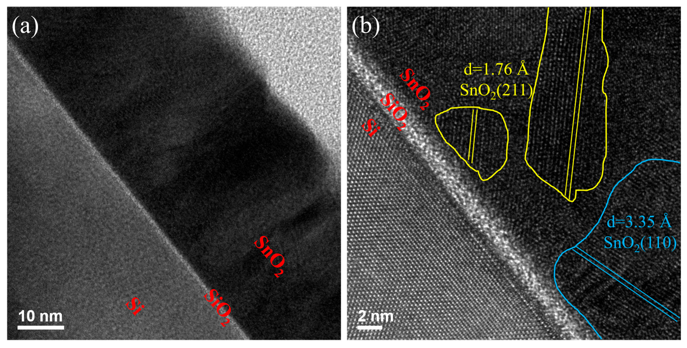
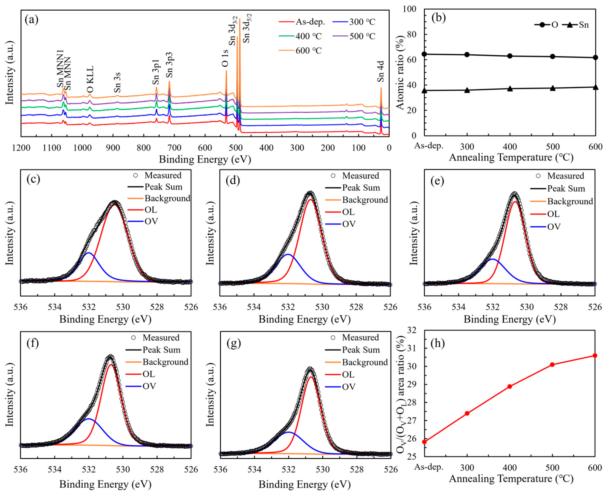
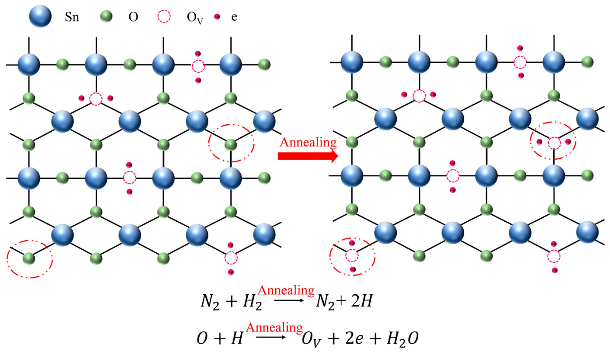
3. Results and Discussion

The grazing incidence X-ray diffraction (GIXRD) patterns of SnO2 films subjected to annealing at various temperatures are shown in Figure 1a and were analyzed to investigate their crystalline structure. The XRD analysis revealed that higher annealing temperatures promoted crystallization of the SnO2 films, evidenced by the emergence and sharpening of characteristic diffraction peaks. The intensity of these peaks increased with higher crystallinity. Diffraction peaks were observed at 2θ = 26.98°, 31.14°, 38.18°, and 52.06°, corresponding to the (110), (101), (111), and (211) planes of SnO2, respectively, as indexed in the standard JCPDS database (No. 06-0318). Additionally, with increasing annealing temperature, the full width at half maximum (FWHM) of the diffraction peaks decreased from 7.29° at 300 °C to 1.69° at 600 °C, as shown in Figure 1b, indicating an increase in grain size. Scherrer equation calculations revealed that the grain size grew from 1.23 nm at 300 °C to 5.30 nm at 600 °C [29,30]. The peak positions remained stable across all annealing conditions, suggesting that no significant changes occurred in the lattice parameters. Furthermore, the diffraction peaks became sharper and more symmetrical, indicating a more well-ordered crystal structure with fewer defects.
Figure 2a–e show the surface morphology of SnO2 thin films annealed at different temperatures, as observed by top-view SEM (scale bar: 200 nm). The films were deposited on Si substrates. At lower annealing temperatures, the surface exhibits notable agglomeration, where small nanocrystalline domains tend to cluster into larger, irregularly shaped aggregates. With increasing annealing temperature, these aggregates are significantly reduced, and the surface becomes smoother and more uniform, indicating enhanced film densification and improved morphological uniformity [31,32,33]. Although no distinct crystalline grains are visible in the SEM images, this morphological evolution is consistent with the XRD results, which show a gradual decrease in the FWHM of diffraction peaks—suggesting enhanced crystallinity and grain growth. These findings imply that N2/H2 annealing not only reduces surface agglomeration but also promotes structural ordering at the nanoscale.
To evaluate the microstructural characteristics of the SnO2 thin films annealed at 600 °C, cross-sectional TEM was performed at magnifications of 300 K and 800 K. The samples consist of a Si substrate with an interfacial SiO2 layer of approximately 2 nm, serving as a buffer between the substrate and the SnO2 film. At low magnification (300 K), as shown in Figure 3a, the overall film structure is clearly observed, with a uniform SnO2 layer atop the Si/SiO2 interface. The SiO2 interlayer appears as a continuous, amorphous contrast layer between the crystalline Si substrate and the polycrystalline SnO2 film. Figure 3b presents high-resolution TEM (800 K magnification) images showing well-ordered lattice fringes in the SnO2 film, further evidencing the improved crystallinity achieved through thermal treatment. The measured lattice spacings are approximately 0.334 nm and 0.263 nm, which correspond to the (110) and (211) crystal planes of tetragonal rutile SnO2 (JCPDS No. 06-0318), respectively. These planes are clearly marked in the image, confirming the oriented grain growth and crystalline nature of the film. The presence of sharp interfaces and well-ordered lattice structures suggests that annealing at 600 °C effectively promotes SnO2 crystallization while preserving the integrity of the interfacial SiO2 layer. Such structural improvements are expected to enhance carrier mobility and are consistent with the observed electrical performance improvements.
The X-ray photoelectron spectroscopy (XPS) survey spectra of SnO2 films annealed at different temperatures are given in Figure 4a, which exhibit distinct peaks corresponding to Sn and O, with no detectable additional impurity peaks, indicating high sample preparation purity and no introduction of unexpected impurities. Figure 4b illustrates the variation in atomic concentrations of Sn and O in the SnO2 films as a function of annealing temperature. As the temperature increases, the atomic percentage of Sn exhibits a gradual rise, whereas that of O shows a corresponding decline. Consequently, the O/Sn atomic ratio decreases from 1.80 at 300 °C to 1.61 at 600 °C. This trend suggests a progressive loss of oxygen, which is indicative of the formation of oxygen vacancies. Figure 4c–g display the high-resolution O 1s XPS spectra of SnO2 thin films subjected to annealing at various temperatures. The broad peak profiles indicate the presence of multiple oxygen-related chemical states. Deconvolution of the O 1s spectra reveals two distinct components: a peak at 530.1 eV corresponding to lattice oxygen (OL), and another at 531.1 eV associated with oxygen vacancies (OV). As illustrated in Figure 4 h, the area ratio of OV to the total oxygen content [OV/(OV + OL)] increases with rising annealing temperature. Specifically, the OV/(OV + OL) ratio of the as-deposited SnO2 film is 25.81%, and this value gradually rises to 30.59% with increasing annealing temperature from 300 °C to 600 °C, indicating an enhancement in oxygen vacancy concentration induced by thermal treatment. This trend indicates that hydrogen in the N2/H2 (95:5) annealing atmosphere acts as a reducing agent, reacting with lattice oxygen to generate H2O and oxygen vacancies. This mechanism is further supported by the observed decrease in overall oxygen content (Figure 4b), confirming that high-temperature annealing under reducing conditions facilitates the formation of oxygen vacancies in SnO2 thin films.
To further elucidate the origin of oxygen vacancies (OVs) in the SnO2 films annealed under a reducing atmosphere, a schematic diagram is presented in Figure 5. During annealing in a nitrogen–hydrogen (N2/H2) ambient atmosphere, hydrogen molecules diffuse to the film surface and react with lattice oxygen atoms (OL) in the SnO2 crystal. This reaction forms gaseous H2O, which desorbs from the lattice, thereby removing lattice oxygen and generating oxygen vacancies (OVS). The creation of oxygen vacancies releases free electrons, which act as shallow donors and contribute to the increased carrier concentration. The overall reaction can be expressed as follows:
OL (lattice oxygen) + H2 → H2O (gas) + OV (oxygen vacancy)
This mechanism aligns with the XPS results shown in Figure 4b,h, where a clear reduction in the O/Sn atomic ratio and an increase in the OV/(OV + OL) peak area ratio are observed with increasing annealing temperature.
Hall effect measurements were employed to investigate the electrical characteristics of the SnO2 thin films, with the results summarized in Figure 6. To ensure accurate electrical characterization, Hall measurements were performed on SnO2 films deposited on insulating glass substrates, thereby eliminating any electrical contribution from the substrate. The thickness values used to calculate the carrier concentration were determined using spectroscopic ellipsometry. For the as-deposited film, the initial thickness was approximately 41.26 nm. Since annealing could cause mild surface etching, the film thickness was remeasured after each annealing condition. The updated thickness values—39.89 nm (300 °C), 40.53 nm (400 °C), 41.56 nm (500 °C), and 39.31 nm (600 °C)—were used in the Hall analysis to ensure accurate estimation of carrier concentrations. This analysis provides insight into the variations in resistivity, carrier concentration, and mobility as a function of annealing temperature. The carrier concentration exhibited a significant increase with rising annealing temperature, rising from 8.05 × 10¹⁹ to 3.37 × 1020 cm−3. This enhancement is attributed to the elevated concentration of oxygen vacancies, as confirmed by XPS analysis. These vacancies act as shallow donors, supplying free electrons to the conduction band and thereby improving n-type conductivity. The Hall mobility also exhibits a positive correlation with annealing temperature, increasing from 1.93 to 7.19 cm2/V·s. This improvement is likely associated with grain growth, enhanced crystallinity, and reduced carrier scattering. Correspondingly, the resistivity, depicted in Figure 6b, shows a pronounced reduction from 4.02 × 10⁻² Ω·cm to 2.58 × 10⁻³ Ω·cm as the annealing temperature increases. These improvements in electrical performance are particularly beneficial for SnO2 when employed as ETLs in PSCs. Higher carrier concentration and mobility facilitate more efficient electron extraction and suppress charge recombination at the interface, thereby contributing to improved fill factors and overall device efficiency.
To explore the influence of different gas environments on the electrical properties of SnO2 thin films, annealing was carried out in six different atmospheres at 600 °C: pure argon, forming gas (N2:H2 = 95%:5%), vacuum, oxygen, ozone, and air. The purpose was to compare the effects of reducing and oxidizing environments. The results, shown in Table 2, demonstrate that reducing atmospheres significantly increased the carrier concentration, whereas oxidizing conditions tended to reduce carrier concentration but improve mobility. Notably, N2:H2 annealing yielded the highest carrier concentration (3.37 × 1020 cm−3) and lowest resistivity (2.58 × 10⁻³ Ω·cm), indicating enhanced electrical performance under moderately reducing conditions. It provides a comprehensive insight into gas-environment-dependent tuning of SnO2 films and validates the potential of forming gas annealing for optimizing electron transport layers in transparent conductive oxide (TCO) applications.
To further validate the electrical advantages of the SnO2 films developed in this work, a comparative analysis was performed against previously reported films fabricated by using various deposition methods and subjected to post-annealing, as summarized in Table 3 [34,35,36,37,38]. The SnO2 films prepared via PEALD and annealed at 600 °C in a N2/H2 atmosphere exhibit a significantly lower resistivity (2.58 × 10⁻³ Ω·cm) and a much higher carrier concentration (7.19 × 1020 cm−3) than most reported counterparts. This superior conductivity is primarily attributed to the increased concentration of oxygen vacancies induced by high-temperature annealing in a reducing ambient atmosphere, as confirmed by XPS analysis. Although the Hall mobility (7.19 cm2/V·s) is relatively lower compared to films deposited by sputtering, pulsed laser deposition (PLD), sol–gel processes, and thermal ALD, the overall electrical performance—particularly the ultra-low resistivity and high carrier density—demonstrates the effectiveness of the PEALD approach in optimizing film conductivity. These results suggest that PEALD-derived SnO2 films, with their excellent charge transport properties and interface quality, hold strong potential as ETLs in PSCs and other advanced optoelectronic devices.

4. Conclusions

This study demonstrates that PEALD-grown SnO2 thin films, when subjected to post-annealing in a N2/H2 atmosphere, exhibit significantly enhanced structural and electrical properties. With increasing annealing temperature, the films transitioned from amorphous to crystalline phases, showing improved grain size, crystallinity, and surface uniformity. XPS analysis revealed an increase in oxygen vacancies, which acted as shallow donors and contributed to a substantial rise in carrier concentration. Hall measurements confirmed that resistivity decreased to 2.58 × 10⁻³ Ω·cm and carrier concentration increased to 3.37 × 1020 cm−3. Overall, the results highlight that PEALD combined with reducing-atmosphere annealing is an effective strategy for engineering high-quality SnO2 thin films, offering great potential for use as ETLs in PSCs and other advanced optoelectronic devices.

Author Contributions

Conceptualization, C.-N.C. and S.-Y.L.; methodology, Z.-X.Z.; validation, Z.-X.Z., W.-Q.F., J.-R.D. and Y.-X.Y.; formal analysis, Q.-Z.C., Z.-X.Z., W.-Q.F., J.-R.D. and Y.-X.Y.; investigation, Q.-Z.C. and Z.-X.Z.; writing—original draft, Z.-X.Z.; writing—review and editing, Q.-Z.C.; supervision, S.-Y.L.; funding acquisition, Q.-Z.C. and S.-Y.L. All authors have read and agreed to the published version of the manuscript.

Funding

This study is partially sponsored by the Natural Science Foundation of Xiamen (3502Z20227065), in part by the Natural Science Foundation of Fujian Province (2023J011457), in part by the National Natural Science Foundation of China (62304190), and in part by the Science Project of Xiamen University of Technology (YKJ22032R).

Data Availability Statement

The data are contained within the article.

Conflicts of Interest

The authors declare no conflicts of interest.

References

  1. Yoo, J.J.; Shin, S.S.; Seo, J. Toward Efficient Perovskite Solar Cells: Progress, Strategies, and Perspectives. ACS Energy Lett. 2022, 7, 2084–2091. [Google Scholar] [CrossRef]
  2. Nazir, G.; Lee, S.; Lee, J.; Rehman, A.; Lee, J.; Seok, S.I.; Park, S. Stabilization of Perovskite Solar Cells: Recent Developments and Future Perspectives. Adv. Mater. 2022, 34, 2204380. [Google Scholar] [CrossRef] [PubMed]
  3. Yan, J.; Savenije, T.J.; Mazzarella, L.; Isabella, O. Progress and Challenges on Scaling up of Perovskite Solar Cell Technology. Sustain. Energy Fuels 2022, 6, 243–266. [Google Scholar] [CrossRef]
  4. Roy, P.; Ghosh, A.; Barclay, F.; Khare, A.; Cuce, E. Perovskite Solar Cells: A Review of the Recent Advances. Coatings 2022, 12, 1089. [Google Scholar] [CrossRef]
  5. Yoo, J.J.; Seo, G.; Chua, M.R.; Park, T.G.; Lu, Y.; Rotermund, F.; Kim, Y.-K.; Moon, C.S.; Jeon, N.J.; Correa-Baena, J.-P.; et al. Efficient Perovskite Solar Cells via Improved Carrier Management. Nature 2021, 590, 587–593. [Google Scholar] [CrossRef]
  6. Uddin, A.; Yi, H. Progress and Challenges of SnO2 Electron Transport Layer for Perovskite Solar Cells: A Critical Review. Sol. RRL 2022, 6, 2100983. [Google Scholar] [CrossRef]
  7. Min, H.; Lee, D.Y.; Kim, J.; Kim, G.; Lee, K.S.; Kim, J.; Paik, M.J.; Kim, Y.K.; Kim, K.S.; Kim, M.G.; et al. Perovskite Solar Cells with Atomically Coherent Interlayers on SnO2 Electrodes. Nature 2021, 598, 444–450. [Google Scholar] [CrossRef]
  8. Xiong, Z.; Lan, L.; Wang, Y.; Lu, C.; Qin, S.; Chen, S.; Zhou, L.; Zhu, C.; Li, S.; Meng, L.; et al. Multifunctional Polymer Framework Modified SnO2 Enabling a Photostable α-FAPbI3 Perovskite Solar Cell with Efficiency Exceeding 23%. ACS Energy Lett. 2021, 6, 3824–3830. [Google Scholar] [CrossRef]
  9. Chen, Y.; Zuo, X.; He, Y.; Qian, F.; Zuo, S.; Zhang, Y.; Liang, L.; Chen, Z.; Zhao, K.; Liu, Z.; et al. Dual Passivation of Perovskite and SnO2 for High-Efficiency MAPbI3 Perovskite Solar Cells. Adv. Sci. 2021, 8, 2001466. [Google Scholar] [CrossRef]
  10. Kim, M.; Jeong, J.; Lu, H.; Lee, T.K.; Eickemeyer, F.T.; Liu, Y.; Choi, I.W.; Choi, S.J.; Jo, Y.; Kim, H.-B.; et al. Conformal Quantum Dot–SnO2 Layers as Electron Transporters for Efficient Perovskite Solar Cells. Science 2022, 375, 302–306. [Google Scholar] [CrossRef]
  11. Park, S.Y.; Zhu, K. Advances in SnO2 for Efficient and Stable n–i–p Perovskite Solar Cells. Adv. Mater. 2022, 34, 2110438. [Google Scholar] [CrossRef] [PubMed]
  12. Song, J.W.; Shin, Y.S.; Kim, M.; Lee, J.; Lee, D.; Seo, J.; Lee, Y.; Lee, W.; Kim, H.; Mo, S.; et al. Post-Treated Polycrystalline SnO2 in Perovskite Solar Cells for High Efficiency and Quasi-Steady-State-IV Stability. Adv. Energy Mater. 2024, 14, 2401753. [Google Scholar] [CrossRef]
  13. Pramitha, A.; Rao, S.G.; Raviprakash, Y. Modulating the Properties of SnO2 Thin Film by Post-Deposition UV-Ozone Treatment. J. Electron. Mater. 2023, 52, 8124–8131. [Google Scholar] [CrossRef]
  14. Wang, C.-M.; Huang, C.-C.; Kuo, J.-C.; Sahu, D.; Huang, J.-L. Effect of Annealing Temperature and Oxygen Flow in the Properties of Ion Beam Sputtered SnO—2x Thin Films. Materials 2015, 8, 5289–5297. [Google Scholar] [CrossRef]
  15. Mao, K.; Cai, F.; Zhu, Z.; Meng, H.; Li, T.; Yuan, S.; Zhang, J.; Peng, W.; Xu, J.; Feng, X.; et al. Unveiling and Balancing the Passivation-Transport Trade-Off in Perovskite Solar Cells with Double-Side Patterned Insulator Contacts. Adv. Energy Mater. 2023, 13, 2302132. [Google Scholar] [CrossRef]
  16. Chen, C.; Chen, J.; Han, H.; Chao, L.; Hu, J.; Niu, T.; Dong, H.; Yang, S.; Xia, Y.; Chen, Y.; et al. Perovskite Solar Cells Based on Screen-Printed Thin Films. Nature 2022, 612, 266–271. [Google Scholar] [CrossRef]
  17. Gil-Escrig, L.; Roß, M.; Sutter, J.; Al-Ashouri, A.; Becker, C.; Albrecht, S. Fully Vacuum-Processed Perovskite Solar Cells on Pyramidal Microtextures. Sol. RRL 2021, 5, 2000553. [Google Scholar] [CrossRef]
  18. Heffner, H.; Du, Y.; Shilovskikh, V.; Taretto, K.; Wrzesińska-Lashkova, A.; Soldera, M.; Lasagni, A.F.; Vaynzof, Y. Direct Laser Interference Patterning of Fluorine-Doped Tin Oxide as a Pathway to Higher Efficiency in Perovskite Solar Cells. Adv Funct Mater. 2025, 35, 2415126. [Google Scholar] [CrossRef]
  19. Castillo-Saenz, J.; Nedev, N.; Valdez-Salas, B.; Curiel-Alvarez, M.; Mendivil-Palma, M.I.; Hernandez-Como, N.; Martinez-Puente, M.; Mateos, D.; Perez-Landeros, O.; Martinez-Guerra, E. Properties of Al2O3 Thin Films Grown by PE-ALD at Low Temperature Using H2O and O2 Plasma Oxidants. Coatings 2021, 11, 1266. [Google Scholar] [CrossRef]
  20. Lee, D.-K.; Wan, Z.; Bae, J.-S.; Lee, H.-B.-R.; Ahn, J.-H.; Kim, S.-D.; Kim, J.; Kwon, S.-H. Plasma-Enhanced Atomic Layer Deposition of SnO2 Thin Films Using SnCl4 and O2 Plasma. Mater. Lett. 2016, 166, 163–166. [Google Scholar] [CrossRef]
  21. Chen, Q.-Z.; Shi, C.-Y.; Zhao, M.-J.; Gao, P.; Wu, W.-Y.; Wuu, D.-S.; Horng, R.-H.; Lien, S.-Y.; Zhu, W.-Z. Performance of Transparent Indium–Gallium–Zinc Oxide Thin Film Transistor Prepared by All Plasma Enhanced Atomic Layer Deposition. IEEE Electron Device Lett. 2023, 44, 448–451. [Google Scholar] [CrossRef]
  22. Yin, C.; Zhu, M.; Song, C.; Zeng, T.; Xu, N.; Wang, Y.; Zhao, Y.; Yi, K.; Shao, J. Influence of Deposition Temperature and Precursor Pulse Time on Properties of SiO2, HfO2 Monolayers Deposited by PEALD. In Proceedings of the Tenth International Conference on Thin Film Physics and Applications (TFPA 2019), Qingdao, China, 8 July 2019; SPIE: Qingdao, China, 2019; p. 39. [Google Scholar]
  23. Kim, W.-H.; Maeng, W.J.; Moon, K.-J.; Myoung, J.-M.; Kim, H. Growth Characteristics and Electrical Properties of La2O3 Gate Oxides Grown by Thermal and Plasma-Enhanced Atomic Layer Deposition. Thin Solid Film. 2010, 519, 362–366. [Google Scholar] [CrossRef]
  24. Xu, L.; Zhang, Z.; Yang, L.; Yang, J.; Wang, P.; Gao, G.; Sun, C.; Ralchenko, V.; Zhu, J. Comparison of Thermal, Plasma-Enhanced and Layer by Layer Ar Plasma Treatment Atomic Layer Deposition of Tin Oxide Thin Films. J. Cryst. Growth 2021, 572, 126264. [Google Scholar] [CrossRef]
  25. Bae, J.; Jeon, H. Effects of Deposition and Annealing Temperature on Atomic Layer-Deposited Tin Dioxide Thin Films. J. Korean Phys. Soc. 2025. [Google Scholar] [CrossRef]
  26. Liu, S.; Li, Y.; Tao, J.; Tang, R.; Zheng, X. Structural, Surface, and Optical Properties of AlN Thin Films Grown on Different Substrates by PEALD. Crystals 2023, 13, 910. [Google Scholar] [CrossRef]
  27. Blanco, E.; Domínguez, M.; González-Leal, J.M.; Márquez, E.; Outón, J.; Ramírez-del-Solar, M. Insights into the Annealing Process of Sol-Gel TiO2 Films Leading to Anatase Development: The Interrelationship between Microstructure and Optical Properties. Appl. Surf. Sci. 2018, 439, 736–748. [Google Scholar] [CrossRef]
  28. Chen, K.-T.; Hsu, C.-H.; Ren, F.-B.; Wang, C.; Gao, P.; Wu, W.-Y.; Lien, S.-Y.; Zhu, W.-Z. Influence of Annealing Temperature of Nickel Oxide as Hole Transport Layer Applied for Inverted Perovskite Solar Cells. J. Vac. Sci. Technol. A Vac. Surf. Film. 2021, 39, 062401. [Google Scholar] [CrossRef]
  29. Wu, S.; Li, C.; Lien, S.Y.; Gao, P. Temperature Matters: Enhancing Performance and Stability of Perovskite Solar Cells through Advanced Annealing Methods. Chemistry 2024, 6, 207–236. [Google Scholar] [CrossRef]
  30. Ling, P.S.V.; Hagfeldt, A.; Sanchez, S. Flash Infrared Annealing for Perovskite Solar Cell Processing. JoVE 2021, 61730. [Google Scholar] [CrossRef]
  31. Yıldırım, M.A.; Akaltun, Y.; Ateş, A. Characteristics of SnO2 Thin Films Prepared by SILAR. Solid State Sci. 2012, 14, 1282–1288. [Google Scholar] [CrossRef]
  32. Yang, Y.; Maeng, B.; Jung, D.G.; Lee, J.; Kim, Y.; Kwon, J.; An, H.K.; Jung, D. Annealing Effects on SnO2 Thin Film for H2 Gas Sensing. Nanomaterials 2022, 12, 3227. [Google Scholar] [CrossRef] [PubMed]
  33. Mehraj, S.; Ansari, M.S. Alimuddin Annealed SnO2 Thin Films: Structural, Electrical and Their Magnetic Properties. Thin Solid Films 2015, 589, 57–65. [Google Scholar] [CrossRef]
  34. Zhang, L.; Xu, W.; Liu, W.; Cao, P.; Han, S.; Zhu, D.; Lu, Y. Structural, Chemical, Optical, and Electrical Evolution of Solution-Processed SnO2 Films and Their Applications in Thin-Film Transistors. J. Phys. D Appl. Phys. 2020, 53, 175106. [Google Scholar] [CrossRef]
  35. Mun, H.; Yang, H.; Park, J.; Ju, C.; Char, K. High Electron Mobility in Epitaxial SnO2−x in Semiconducting Regime. APL Mater. 2015, 3, 076107. [Google Scholar] [CrossRef]
  36. Lee, G.R.; Seong, M.; Kim, S.; Pyeon, K.; Chung, R.B. Conductive SnO2−x Thin Films Deposited by Thermal ALD with H2O Reactant. Vacuum 2022, 200, 111018. [Google Scholar] [CrossRef]
  37. Yu, S.; Li, L.; Sun, Z.; Zheng, H.; Dong, H.; Xu, D.; Zhang, W. Characteristics of Transparent Conducting W-Doped SnO2 Thin Films Prepared by Using the Magnetron Sputtering Method. J. Am. Ceram. Soc. 2015, 98, 1121–1127. [Google Scholar] [CrossRef]
  38. Brousseau, J.-L.; Bourque, H.; Tessier, A.; Leblanc, R.M. Electrical Properties and Topography of SnO2 Thin Films Prepared by Reactive Sputtering. Appl. Surf. Sci. 1997, 108, 351–358. [Google Scholar] [CrossRef]
Figure 1. (a) XRD patterns and (b) FWHM and crystallite size of SnO2 films at different annealing temperatures.
Nanomaterials 15 00986 g001
Figure 2. Topographical SEM images of SnO2 thin films at different annealing temperatures: (a) as-deposited SnO2 film, (b) SnO2 film annealed at 300 °C, (c) SnO2 film annealed at 400 °C (d) SnO2 film annealed at 500 °C, and (e) SnO2 film annealed at 600 °C.
Nanomaterials 15 00986 g002
Figure 3. Cross-sectional transmission electron microscopy (TEM) images of the Si/buffer/SnO2 multilayer structure annealed at 600 °C in a N2/H2 atmosphere: (a) low magnification and (b) high magnification.
Nanomaterials 15 00986 g003
Figure 4. (a) XPS survey spectra of SnO2 films; (b) atomic ratio of Sn to O at different annealing temperatures; high-resolution O 1s spectra of (c) as-deposited SnO2 film; (d) SnO2 film annealed at 300 °C; (e) SnO2 film annealed at 400 °C; (f) SnO2 film annealed at 500 °C; (g) SnO2 film annealed at 600 °C; and (h) the OV peak area ratio of the SnO2 films at different annealing temperatures.
Nanomaterials 15 00986 g004
Figure 5. A schematic mechanism of annealing-induced properties.
Nanomaterials 15 00986 g005
Figure 6. (a) Carrier concentration, mobility, and (b) resistivity of SnO2 thin films at different annealing temperatures.
Nanomaterials 15 00986 g006
Table 1. Preparation parameters of PEALD-SnO2 thin films.
ParameterValue
Bubbler temperature (°C)50
Substrate temperature (°C)200
TDMASn pulse time (s)1.6
TDMASn purge time (s)6
O2 pulse time (s)11
O2 purge time (s)5
Ar flow rate (sccm)80
O2 flow rate (sccm)150
O2 plasma power (W)2500
TDMASn carry gas flow rate (sccm)120
TDMASn dilute gas flow rate (sccm)400
Post-annealing temperature (°C)300–600
Post-annealing gas N2 (95%) + H2 (5%)
Post-annealing gas flow rate (L/min)3
Table 2. Electrical properties of SnO2 films annealed in different atmospheres at 600 °C.
Annealing AtmosphereCarrier Concentration (cm−3)Mobility
(cm2/V·s)
Resistivity
(Ω·cm)
N2:H23.37 × 10207.192.58 × 10−3
Argon1.03 × 10206.539.25 × 10−3
Vacuum2.58 × 10203.227.52 × 10−3
Oxygen3.15 × 101915.231.30 × 10−2
Ozone5.78 × 101819.465.60 × 10−2
Air1.03 × 10199.416.46 × 10−2
Table 3. Comparison of electrical properties of SnO2 films prepared via different deposition methods after annealing.
Deposition MethodAnnealing ConditionsR
(Ω·cm)
n
(cm−3)
Mobility
(cm2/V·s)
T (nm)Ref.
sol–gelAir, 700 °C, 2 h72.676.25 × 101513.730.8[34]
PLDO2, 600 °C1.97 × 10–23 × 1018106700[35]
MSNone (600 °C substrate heating)1.75 × 10−31.6 × 102022.48300[37]
DCNone (150 °C substrate heating)4.5 × 10−38.9 × 101920.7712.5[38]
thermal ALDN2, 400 °C, 1 h~8.8 × 10–33.3 × 101921.5520[36]
PEALDN2/H2 (95:5), 600 °C, 1 h,2.58 × 10–33.37 × 10207.1940This work
Ref. = reference; n = carrier concentration; R = resistivity; MS = magnetron sputtering; DC = DC sputtering; T = thickness.
Disclaimer/Publisher’s Note: The statements, opinions and data contained in all publications are solely those of the individual author(s) and contributor(s) and not of MDPI and/or the editor(s). MDPI and/or the editor(s) disclaim responsibility for any injury to people or property resulting from any ideas, methods, instructions or products referred to in the content.

