Article

Barrier-Free Carrier Injection in 2D WSe2-MoSe2 Heterostructures via Fermi-Level Depinning

1
School of Electronic Information Engineering, Guiyang University, Guiyang 550005, China
2
School of Physics and Electronic Science, Guizhou Normal University, Guiyang 550025, China
3
School of Integrated Circuit, Guizhou Normal University, Guiyang 550025, China
*
Authors to whom correspondence should be addressed.
Nanomaterials 2025, 15(13), 1035; https://doi.org/10.3390/nano15131035
Submission received: 3 June 2025 / Revised: 30 June 2025 / Accepted: 2 July 2025 / Published: 3 July 2025
(This article belongs to the Section Nanoelectronics, Nanosensors and Devices)

Abstract

Fermi-level pinning (FLP) at metal–semiconductor interfaces remains a key obstacle to achieving low-resistance contacts in two-dimensional (2D) transition metal dichalcogenide (TMDC)-based heterostructures. Here, we present a first-principles study of Schottky barrier formation in WSe2-MoSe2 van der Waals heterostructures interfaced with four representative metals (Ag, Al, Au, and Pt). It was found that all metal–WSe2/MoSe2 direct contacts induce pronounced metal-induced gap states (MIGSs), leading to significant FLP inside the WSe2/MoSe2 band gaps and elevated Schottky barrier heights (SBHs) greater than 0.31 eV. By introducing a 2D metal-doped metallic (mWSe/mMoSe) layer between WSe2/MoSe2 and the metal electrodes, the MIGSs can be effectively suppressed, resulting in nearly negligible SBHs for both electrons and holes, with even an SBH of 0 eV observed in the Ag-AgMoSe-MoSe2 contact, thereby enabling quasi-Ohmic contact behavior. Our results offer a universal and practical strategy to mitigate FLP and achieve high-performance TMDC-based electronic devices with ultralow contact resistance.

Graphical Abstract

1. Introduction

Among various two-dimensional (2D) materials, transition metal dichalcogenides (TMDCs) are attracting tremendous interest due to their promising applications in electronics [1,2], valleytronics [3], optoelectronics [4,5], and spintronics [6]. Specifically, the dangling bond-free surfaces of 2D TMDCs enable the flexible construction of van der Waals (vdWs) heterostructures, providing opportunities for new devices to be developed with advanced functions. Observing moiré superlattice exciton states in WSe2-WS2 vdWs heterostructures experimentally provides an attractive platform for controlling excited states of matter [7]. Tunneling field effect transistors based on 2D TMDC heterostructures, with a subthreshold swing of less than 60 mV dec−1, have been previously demonstrated [8,9]. Intriguingly, type II heterostructures can be constructed by employing appropriate TMDC layers, which enable the ultrafast dynamics of charge transfer across the vdWs interface and allow for the spatial segregation of photo-generated holes and electrons to be achieved. With 99% charge transfer efficiency, electrons can be transferred from WSe2 to MoS2 within 470 fs in MoS2-WSe2 p-n heterojunctions [10]. Policht et al. reported an ultrafast interlayer electron transfer time of up to 69 femtoseconds in a WS2-MoS2 heterostructure with type II band alignment, as revealed by two-dimensional electronic spectroscopy [11]. Similar sub-ps level charge transfer processes were also demonstrated in MoS2-MoTe2, MoSe2-MoS2 and WSe2-WS2 heterostructures [12,13]. However, when these heterojunctions are integrated into optoelectronic devices, the photoresponse times increase to the microsecond scale [14,15].
Inevitably, 2D TMDC-based devices have contact interfaces with metal electrodes, and the quality of the electrical contacts becomes particularly important for their performance. Unfavorable band edges are usually presented in 2D TMDCs due to the strong excitonic effect and quantum confinement [16]; thus, for most available metals, the work function varies from 3.5 eV to 5.7 eV [17]. The formation of low-resistance Ohmic contacts that do not obscure the intrinsic exceptional properties of two-dimensional (2D) TMDCs remains a significant challenge [18]. The Schottky barrier height (SBH) at metal–2D TMDC interfaces, influenced by complex Fermi-level pinning (FLP), does not solely depend on the difference between the metal work function and the valence band maximum (VBM) or conduction band minimum (CBM) of the TMDC. This presents a significant obstacle to efficient charge injection. A large SBH leads to high contact resistance at the metal–TMDC interfaces, reducing the carrier injection efficiency [19,20]. Therefore, it is highly desirable to decrease SBH to gain high performance for a device.
A Schottky pinning factor S is normally introduced to describe the strength of the FLP, which is defined as the change in SBH (ΦSBH) with respect to the metal work function (WF), i.e., S = |dΦSBH/dWF| [17,21,22]. Note that S is the slope of ΦSBH versus WF, typical values reported are in the range of 0~1 [17,21,22,23], where a value close to 0 corresponds to a strong pinning interface, and a weakly interacting metal–TMDC system is achieved for S close to 1, indicating the ideal Schottky–Mott limit. The FLP effects can normally be attributed to the interfacial effects [24], surface traps [25], and metal-induced gap states (MIGSs) [24,26,27]. Several studies have reported that the FLP can be weakened by inserting a buffer layer between the TMDCs and metal experimentally and theoretically, such as hexagonal boron nitride (h-BN) [28,29], molybdenum trioxide (MoOx, x < 3) [30], ultrathin TiO2 [31], graphene [32,33], ZnO [34], monolayer (ML) NbS2 [25], VS2 [26], and more. These results show that introducing buffer layers is an effective strategy to break the direct metal–TMDC interaction and eliminate the interface states, improving the contact properties.
In addition to their well-established advantages in ultrafast optoelectronics and emerging quantum information technologies [35,36,37], WSe2-MoSe2 heterostructures offer unique opportunities for fundamental studies in interface engineering. By using density functional theory (DFT) simulations, we investigate the interfaces between four conventional metals (Ag, Al, Au, and Pt) and the WSe2 and MoSe2 monolayers within the WSe2-MoSe2 heterostructure. Our results reveal universal Schottky-type contacts characterized by Fermi-level pinning. No ohmic contact is observed; MoSe2 forms an N-type Schottky contact with Ag and Al electrodes, exhibiting electron Schottky barrier heights (SBHs) of 0.31 eV and 0.88 eV, respectively. In contrast, p-type Schottky contacts are formed with Pt and Au electrodes, with hole SBHs of 0.42 and 0.76 eV, respectively. A similar trend is observed for metal–WSe2 interfaces, where the Pt-WSe2 contact exhibits the lowest hole SBH of 0.43 eV. Furthermore, we also demonstrated that inserting a metallic 2D interlayer of mMoSe or mWSe between the metal and the WSe2/MoSe2 layer significantly weakens the interaction at the contact interface. This effectively suppresses the MIGSs, reduces Fermi-level pinning, and substantially reduces all SBHs.

2. Computational Methods

The Projector Augmented Wave (PAW) method and plane-wave basis set implemented in the Vienna ab initio simulation package (VASP) code were employed to optimize the geometries [23,24]. The Perdew Burke Ernzerhof (PBE) exchange correction function under the generalized gradient approximation (GGA) function was utilized [38]. To ensure accuracy, the plane-wave cutoff energy was set as 600 eV. The Brillouin zone was sampled by special k-points of 5 × 5 × 1 for optimizing and 10 × 10 × 1 for densities of state (DOS) calculations [39,40]. The calculations were deemed converged when the energy difference between two successive steps was less than 10−6 eV, and the force acting on each atom is below 0.01 eV/Å. To account for van der Waals (vdW) interactions, we employed the DFT-D3 dispersion correction method developed by Grimme [41].
To accurately model metal electrode interfaces, six atomic layers of (111)-oriented Ag, Al, Au, and Pt slabs were employed, based on surface properties converging in previous studies [42,43]. The in-plane lattice constants of WSe2 and MoSe2 are a1 = 3.29 Å and a2 = 3.32 Å, respectively, demonstrating excellent agreement with experimental measurements [44,45]. To obtain stable heterojunction structures, a supercell with a lattice mismatch of less than 5% was required. Accordingly, pristine metal–WSe2/MoSe2 supercells were constructed using a 2 × 2 expansion of the (111) surfaces of Ag, Al, Au, and Pt, and a√3 × √3 expansion of monolayer (ML) WSe2/MoSe2. This resulted in lattice mismatches ranging from 0.21% to 3.56%, as summarized in Table 1. To eliminate spurious interactions between periodic images, a vacuum layer exceeding 15 Å in thickness was introduced along the z direction.

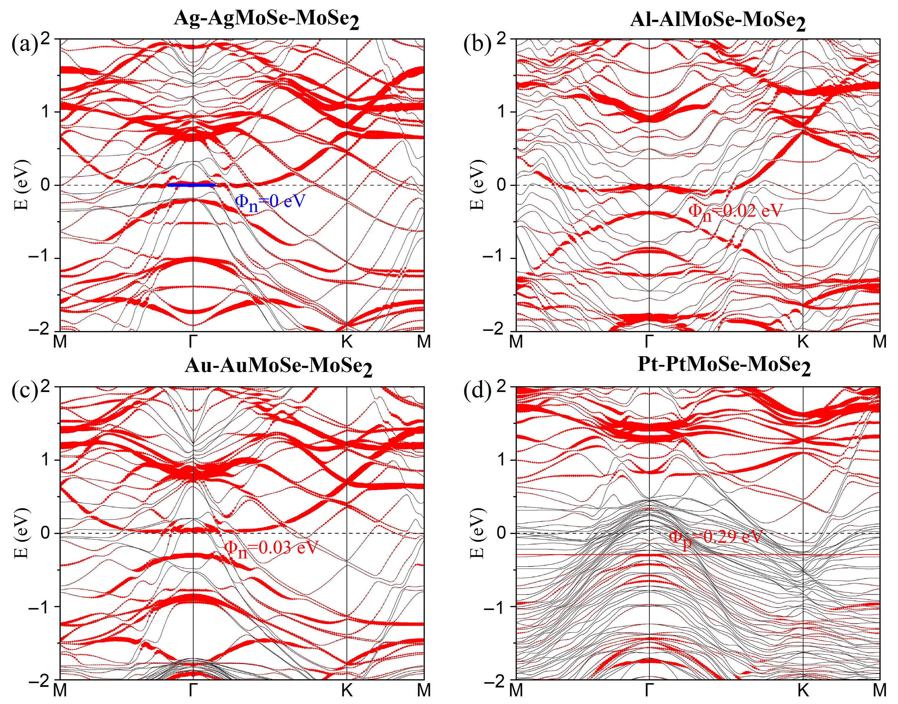
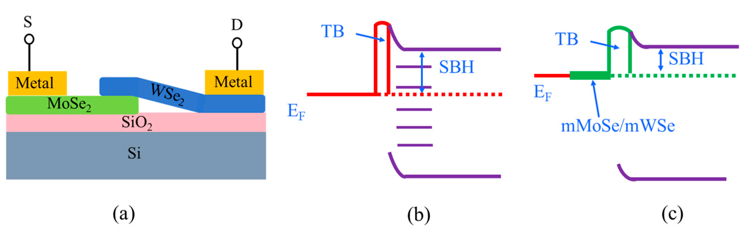
3. Results and Discussion

Figure 1a,b illustrate the op-contact configuration architectures, in which monolayer WSe2/MoSe2 interfaces with six-layer (111)-oriented metal slabs of Al, Ag, Au and Pt. The most stable configuration of the ML WSe2/MoSe2 on Ag and Au corresponds to a geometry in which the Se atoms are located at the center of a hexagons formed by six adjacent surface metal atoms, directly above the surface hollow sites, while the W or Mo atoms are located above the center of a triangle formed by three neighboring metal atoms, as shown in Figure 1a. Figure 1b displays the most stable configuration of Al- and Pt-WSe2/MoSe2 interfaces, where the W or Mo atoms reside above the centers of surface hexagons, and the Se atoms lie above the centers of surface triangles formed by metal atoms. Since previous studies have demonstrated that structural and electronic properties show negligible variation beyond six layers of metal atoms [46], we restrict the slab thickness to six atomic layers. The equilibrium interfacial distances dz, defined as the vertical separation between the Se atoms and the topmost at the interface, range from 2.488 to 2.912 Å, decreasing in the order Al > Au > Ag > Pt (see Table 1). The binding energy per interfacial Se atom is defined as follows:
Eb = (EWSe2/MoSe2 + EmetalEmetal-WSe2/MoSe2)/NSe
Here, Emetal, EWSe2/MoSe2, and Emetal-WSe2/MoSe2 represent the relaxed total energies of the isolated metal surface, WSe2/MoSe2, and the combined system per supercell, respectively; NSe denotes the number of Se atoms at the interface in each supercell. The calculated binding energy Eb ranges from 0.182 eV (Al-WSe2) to 0.342 eV (Pt-MoSe2), as summarized in Table 1, reflecting the trend in bonding strength. Notably, Pt exhibits relatively strong adsorption, with Eb values of 0.318 and 0.342 eV and interfacial distances of 2.53 and 2.488 Å for WSe2/MoSe2, respectively, indicating stronger bonding compared to the other metals.
Prior to investigating the metal–TMDC interface systems, we calculated the band structures of pristine monolayer (ML) MoSe2 and WSe2 (see Figure S1 in the Supplementary Materials). The results confirm that ML WSe2/MoSe2 are semiconductors with band gaps of 1.63 and 1.51 eV, respectively, in good agreement with previously reported values [47,48]. Figure 2 presents the projected band structures of the metal–WSe2 systems, while those for metal–MoSe2 systems are shown in Figure 3. In all cases, the majority of the WSe2 and MoSe2 bands remain discernible upon contact with Ag, Al, Au, and Pt surfaces. Although the conduction bands of MoSe2/WSe2 are well preserved when interfaced with Pt, as shown in Figure 2d and Figure 3d, slight hybridization is observed in the valence bands. This hybridization is attributed to the radius and occupancy of the metal d-orbital [48]. Actually, the degree of band hybridization across the various metal–MoSe2/WSe2 interfaces can be interpreted using the d-band model [49]. Pt, possessing partially filled d-orbitals, forms stronger bonds with MoSe2/WSe2 than Au and Ag, which have fully filled d-shells. These d-orbitals can interact with the d-band edge states of W and Mo, thereby enhancing electron injection efficiency. This observation is consistent with our binding energy calculations. Conversely, Al lacks d-orbitals, resulting in weak bonding with TMDCs [43,47]; accordingly, high contact resistance in Al-TMDC systems has been experimentally verified [50].
Upon contact formation, Schottky barriers arise in the vertical direction. The vertical Schottky barrier height can be precisely determined using Φn = ECBM − EF for electrons and Φp = EF − EVBM for holes, where ECBM, EVBM, and EF represent the conduction band minimum, valence band maximum, and Fermi level of the metal–TMDC junction, respectively. ΦSBH plays a critical role in determining the optical and electronic properties of MoSe2/WSe2 device. As shown in Figure 2a,b, the Ag- and Al-WSe2 interfaces form n-type Schottky contacts, with electron SBHs of Φn = 0.43 and 1.1 eV, respectively. In contrast, the Au- and Pt-WSe2 contacts (see Figure 2c,d) exhibit p-type behavior, with hole SBHs of Φp = 0.66 eV and 0.43 eV. The extracted SBHs values for all metal–WSe2 systems are summarized in Table 1. By using the same approach, we evaluated the SBHs of the metal–MoSe2 systems, as shown in Figure 3, with results also compiled in Table 1. Specifically, the Ag- and Al-MoSe2 interfaces exhibit n-type SBHs of 0.31 eV and 0.88 eV, while the Au- and Pt-MoSe2 contacts exhibit p-type SBHs of 0.76 eV and 0.42 eV, respectively.
Notably, the large Φn value for Al-MoSe2/WSe2 indicates high resistance at the contact interfaces, which is consistent with the previous analysis. The contact polarity of Au-WSe2 has often been reported as ambipolar or p-type [51,52,53]. However, n-type contact behavior can be induced by selenium vacancies [24]. A significant reduction in p-type SBH has been reported for ML WSe2 [52], demonstrating that the SBH value can be tuned by different fabricated techniques. Furthermore, the vertical hole SBHs of Pt-MoSe2/WSe2 systems (0.42/0.43 eV) are comparable to previously reported values of 0.55/0.34 eV [47,48].
Contact engineering is essential for reducing the ΦSBH of the metal–TMDC systems to achieve a low-resistance Ohmic contact in 2D devices. One technologically feasible strategy involves the introduction of an ultrathin buffer layer to lower ΦSBH. For instance, inserting a hexagonal boron nitride (hBN) buffer layer at a Ni-MoS2 interface has been shown to reduce the SBH from 0.158 to 0.031 eV [54]. Similarly, a graphene buffer layer decreases the SBH from 0.3 to 0.19 eV in an Ag-MoS2 configuration [33]. In addition, thin oxide layers such as Al2O3 have been used as a buffer layer at Ti-MoS2 interfaces, reducing the SBH from 0.18 to 0.13 eV [55]. In this study, we propose that metal-doped MoSe2/WSe2 (mMoSe/mWSe) can serve as an effective buffer layer when inserted between metal electrodes and semiconducting MoSe2/WSe2, as illustrated in Figure 1c. A naturally formed van der Waals (vdW) interface exists between the mMoSe/mWSe buffer and the underlying semiconductor layer. Notably, substitutional doping where metal atoms replace Se atoms requires less formation energy and is more thermodynamically favorable than substitution at Mo or W sites. Experimentally, an mMoS layer has been successfully synthesized via a three-step plasma deposition–annealing–yttrium doping process [56]. The transformation of semiconducting MoSe2/WSe2 into metallic mMoSe/mWSe by metal doping was theoretically predicted. As an example, Au doping results in a metallic band structure for AuMoSe2/AuWSe2, with the conduction band minimum (CBM) and valence band maximum (VBM) coinciding in the Brillouin zone, confirming the zero-band gap metallic nature (see Figure S2).
Figure 4a–d show the projected band structures of metal–mWSe–WSe2 heterostructures. The insertion of a 2D mWSe buffer layer at the contact interface reduces the Schottky barrier heights to 0.19, 0.04, 0.13, and 0.19 eV for the Ag-, Al-, Au-, and Pt-mWSe-WSe2 systems, respectively. Similarly, for metal–mMoSe–MoSe2 configurations (Figure 5a–d), the extracted vertical SBHs are 0, 0.02, 0.03, and 0.29 eV, respectively. All extracted electron and hole SBHs are summarized in parentheses in Table 1. It is evident that Φn in n-type contacts is significantly reduced, while Φp in p-type contacts shows only moderate reduction when compared with the corresponding systems without a buffer layer.
Interestingly, in contrast to previous conclusions, the ultralow SBHs observed for Al-mMoSe/mWSe-MoSe2/WSe2 systems demonstrate that Al can become a viable contact metal for low-resistance applications upon inserting a suitable buffer layer. Moreover, a contact polarity transition is observed: while Au-MoSe2/WSe2 interfaces typically exhibit p-type behavior, the corresponding Au-mMoSe/mWSe-MoSe2/WSe2 structures display n-type characteristics. Furthermore, the Ag-mMoSe-MoSe2 system exhibits a vanishing vertical n-type SBH (Figure 5a), indicating the formation of a low-resistance Ohmic or quasi-Ohmic contact, which implies enhanced carrier injection efficiency.
The extracted Schottky barrier heights ΦSBH for various configurations deviate from the values predicted by straightforward band alignment estimations, which can be attributed to the effect of Fermi-level pinning (FLP) at the interfaces. To further quantify the strength of the pinning behavior in different contacts, we plot the dependence of Φn on the metal work function for MoSe2 and WSe2 semiconductor systems, as shown in Figure 6. It is observed that the SBHs for metal–WSe2 interfaces lie along a line with a slope of S = 0.41, while those for metal–MoSe2 interfaces follow a line with a slope of S = 0.33 (Figure 6a). These slopes deviate significantly from the ideal Schottky–Mott limit (S = 1), indicating a strong Fermi-level pinning effect. Notably, these values are considerably larger than those observed in conventional semiconductor systems such as GaAs (S = 0.07) and Si (S = 0.27) [57], highlighting the partial tunability of Fermi-level positioning in TMDCs.
For comparison, Figure 6b shows the extracted pinning factors when a mMoSe/mWSe buffer layer is inserted between the metals and the MoSe2/WSe2 semiconductors. The resulting pinning factors are significantly larger: 0.79 for metal–mMoSe–MoSe2 and 0.76 for metal–mWSe–WSe2, indicating a substantial depinning of the Fermi level. This depinning behavior is attributed to the reduced density of metal-induced gap states (MIGSs) in the contact region, arising from a weakened interaction between the metal electrodes and the MoSe2/WSe2 layers. Previous studies have also shown that increasing the metal–TMDC interlayer distance can effectively suppress MIGSs and thereby contribute to Fermi-level depinning and SBH reduction [23].
To gain deeper insight into the effects of conventional metals and metal-doped layers (mMoSe/mWSe) on monolayer (ML) MoSe2 and WSe2 semiconductors, we calculated the partial density of states (PDOS) for both pristine MoSe2/WSe2 and their corresponding contact systems. As shown in Figure 7a–d, significant metal-induced gap states (MIGSs) appear within the intrinsic band gap of WSe2 upon contact with metal surfaces, in contrast to the pristine WSe2, which shows a clean band gap (see Figure S3). These findings are consistent with previous studies [17,47]. Among the investigated metal contacts, Pt-WSe2 exhibits the most pronounced MIGS distribution within the band gap (Figure 7d), indicating strong interfacial hybridization. This observation aligns well with the degree of band structure hybridization discussed earlier. In contrast, as shown in Figure 7e–h, when a metal-doped metallic mWSe buffer layer is introduced at the interface with ML WSe2, the resulting systems exhibit negligible MIGSs, leading to minimal Fermi-level pinning. This can be attributed to the formation of a native, nearly ideal van der Waals (vdW) interface between the mWSe and WSe2 layers. Moreover, a similar trend is observed in the MoSe2 systems. A comparison of the PDOS between metal–MoSe2 and mMoSe-MoSe2 configurations (see Figure S4 in the Supplementary Materials) reveals consistent behavior, further validating the role of the metallic buffer layer in suppressing interfacial states and reducing Fermi-level pinning.
A prototype electronic/optoelectronic device based on a WSe2-MoSe2 van der Waals (vdW) heterostructure, comprising a source (S), a drain (D), and a heterostructure channel, is illustrated in Figure 8a. The interfacial distance dz, obtained from geometry optimization (Table 1), and a notably high potential drop ΔV, defined as the potential energy above the Fermi level EF at the metal–WSe2/MoSe2 interfaces, are observed (Figure S5), confirming the presence of tunneling barriers (TBs) [17,47].
In evaluating carrier injection efficiency, both tunneling barriers and Schottky barriers are considered. Taking the n-type contact as an example, band alignment diagrams for metal–WSe2/MoSe2 and metal–interlayer–WSe2/MoSe2 stacks are presented in Figure 8b,c, respectively. It is important to emphasize that a narrow tunneling barrier combined with a low Schottky barrier at the metal–TMDC interface is beneficial for enhancing carrier injection efficiency [17,18,47]. In the absence of a buffer layer, a thin or even vanishing tunneling barrier forms at the metal–WSe2/MoSe2 interface, which correlates with the degree of band hybridization (Figure 8b). Although the insertion of an mMoSe or mWSe interlayer introduces a larger interfacial distance due to the non-bonding vdW gap between the interlayer and the monolayer MoSe2/WSe2, this configuration significantly weakens the interfacial interaction. As a result, the formation of metal-induced gap states (MIGSs) is effectively suppressed (Figure 8c), thereby reducing the Schottky barrier heights (SBHs).

4. Conclusions

The strategic modulation of Schottky barrier heights (SBHs) for both carrier polarities constitutes a critical advancement in developing high-efficiency two-dimensional optoelectronic devices. In this work, we systematically investigated the contact interfaces between the constituent monolayers of a WSe2-MoSe2 heterojunction and a set of metals with a wide range of work functions (Ag, Al, Au, and Pt). Our calculation results show that directly contacting WSe2/MoSe2 with various metals results in partial FLP due to the large density of MIGSs, and the electron/hole SBHs can be modulated effectively by varying metals (with relatively large values ranging from 0.31 eV for the Ag-MoSe2 contact to 1.11 eV for the Al-WSe2 contact). A larger value of S close to 1 can be obtained by inserting a metal-doped mWSe/mMoSe layer as a metallic buffer between the metals and the 2D WSe2/MoSe2 semiconductor, suggesting a depinning Fermi-level effect. In the presence of a buffer layer, both the polarities of Au-MoSe2 and Au-WSe2 contacts change from P-type to N-type, and all SBHs can be reduced to a small even negligible value due to the suppression of MIGSs, implying a low-resistance Ohmic contact. Our studies provide a theoretical reference for developing high-performance 2D WSe2-MoSe2 heterostructure devices. Although our study focuses on equilibrium electronic structures, advanced topics like light-induced Floquet states or plasmonic effects in 2D systems could further enrich the understanding of TMDC-based heterostructures and are worth exploring in future work.

Supplementary Materials

The following supporting information can be downloaded at: https://www.mdpi.com/article/10.3390/nano15131035/s1.

Author Contributions

Methodology, X.X., Y.Z. and X.-F.L.; Software, J.S.; Validation, Y.-C.X.; Investigation, X.X. and Z.-Y.F.; Resources, J.S. and X.-F.L.; Data curation, Z.-Y.F. and Z.-Y.Z.; Writing—original draft, T.-J.D.; Writing—review & editing, X.-F.L.; Supervision, T.-J.D., Y.-C.X. and X.-F.L.; Project administration, Y.Z.; Funding acquisition, T.-J.D. All authors have read and agreed to the published version of the manuscript.

Funding

This work was supported by the National Natural Science Foundation of China (No. 62264001), the Provincial Basic Research Program project of Guizhou (Nos. QKHJC-ZK[2022]YB009 and QKHJC-ZK[2022]YB014), the High Level Innovation Talents Project of Guizhou Province (No. ZKHT-GCC[2023]007), and the talent introduction starts-up funds for the scientific research project (GYU-KY-2025) and Guiyang University Multidisciplinary Team Construction Projects in 2025 (Gyxk202502).

Data Availability Statement

The original contributions presented in this study are included in the article/Supplementary Material. Further inquiries can be directed to the corresponding author(s).

Conflicts of Interest

The authors declare no conflicts of interest.

References

  1. An, J.; Zhao, X.; Zhang, Y.; Liu, M.; Yuan, J.; Sun, X.; Zhang, Z.; Wang, B.; Li, S.; Li, D. Perspectives of 2D materials for optoelectronic integration. Adv. Funct. Mater. 2022, 32, 2110119. [Google Scholar] [CrossRef]
  2. Chhowalla, M.; Jena, D.; Zhang, H. Two-dimensional semiconductors for transistors. Nat. Rev. Mater. 2016, 1, 16052. [Google Scholar] [CrossRef]
  3. Long, X.; Deng, X.; Hu, F.; Xie, J.; Lv, B.; Liao, Y.; Wang, W. Tunable valley characteristics of WSe2 and WSe2/VSe2 heterostructure. Appl. Surf. Sci. 2023, 624, 157111. [Google Scholar] [CrossRef]
  4. Dhakal, K.P.; Roy, S.; Jang, H.; Chen, X.; Yun, W.; Kim, H.; Lee, J.; Kim, J. Local strain induced band gap modulation and photoluminescence enhancement of multilayer transition metal dichalcogenides. Chem. Mater. 2017, 29, 5124–5133. [Google Scholar] [CrossRef]
  5. Dai, T.; Liu, Y.; Fan, X.; Liu, X.; Xie, D.; Li, Y. Synthesis of few-layer 2H-MoSe2 thin films with wafer-level homogeneity for high-performance photodetector. Nanophotonics 2018, 7, 1959–1969. [Google Scholar] [CrossRef]
  6. Kurpas, M.; Junior, P.; Gmitra, M.; Fabian, J. Spin-orbit coupling in elemental two-dimensional materials. Phys. Rev. B 2019, 100, 125422. [Google Scholar] [CrossRef]
  7. Jin, C.; Regan, E.C.; Yan, A.; Utama, M.; Wang, D.; Zhao, S.; Qin, Y.; Yang, S.; Zheng, Z.; Taniguchi, K.; et al. Observation of moiré excitons in WSe2/WS2 heterostructure superlattices. Nature 2019, 567, 76–80. [Google Scholar] [CrossRef]
  8. Alam, K. Physical insight and performance metrics of monolayer MX2 heterojunction TFETs. Micro Nano Lett. 2020, 15, 81–85. [Google Scholar] [CrossRef]
  9. Choukroun, J.; Pala, M.; Fang, S.; Kaxiras, E.; Dollfus, P. High performance tunnel field effect transistors based on in-plane transition metal dichalcogenide heterojunctions. Nanotechnology 2018, 30, 025201. [Google Scholar] [CrossRef]
  10. Peng, B.; Yu, G.; Liu, X.; Liu, B.; Liang, X.; Bi, L.; Deng, L.; Sum, T.; Loh, K. Ultrafast charge transfer in MoS2/WSe2 p–n Heterojunction. 2D Mater. 2016, 3, 025020. [Google Scholar] [CrossRef]
  11. Policht, V.R.; Russo, M.; Liu, F.; Trovatallo, C.; Maiuri, M.; Bai, Y.; Zhu, X.; Conte, S.; Cerullo, G. Dissecting interlayer hole and electron transfer in transition metal dichalcogenide heterostructures via two-dimensional electronic spectroscopy. Nano Lett. 2021, 21, 4738–4743. [Google Scholar] [CrossRef] [PubMed]
  12. Conte, S.; Trovatello, C.; Gadermaier, C.; Gerullo, G. Ultrafast photophysics of 2D semiconductors and related heterostructures. Trends Chem. 2020, 2, 28–42. [Google Scholar] [CrossRef]
  13. Jin, C.; Ma, E.; Karni, O.; Regan, E.C.; Wang, F.; Heinz, T.F. Ultrafast dynamics in van der Waals heterostructures. Nat. Nanotechnol. 2018, 13, 994–1003. [Google Scholar] [CrossRef]
  14. Varghese, A.; Saha, D.; Thakar, K.; Jindal, V.; Ghosh, S.; Medhekar, N.; Ghosh, S.; Lodha, S. Near-direct bandgap WSe2/ReS2 type-II pn heterojunction for enhanced ultrafast photodetection and high-performance photovoltaics. Nano Lett. 2020, 20, 1707–1717. [Google Scholar] [CrossRef]
  15. Ornelas, C.D.; Bowman, A.; Walmsley, T.S.; Wang, T.; Andrews, K.; Zhou, Z.; Xu, Y. Ultrafast photocurrent response and high detectivity in two-dimensional MoSe2-based heterojunctions. ACS Appl. Mater. Interfaces 2020, 12, 46476–46482. [Google Scholar] [CrossRef]
  16. Ugeda, M.M.; Bradley, A.J.; Shi, S.; Jornada, F.; Zhang, Y.; Qiu, D.Y.; Ruan, W.; Mo, S.; Hussain, Z.; Wang, F.; et al. Giant bandgap renormalization and excitonic effects in a monolayer transition metal dichalcogenide semiconductor. Nat. Mater. 2014, 13, 1091–1095. [Google Scholar] [CrossRef]
  17. Ding, X.; Zhao, Y.; Xiao, H.; Qiao, L. Engineering Schottky-to-Ohmic contact transition for 2D metal–semiconductor junctions. Appl. Phys. Lett. 2021, 118, 091601. [Google Scholar] [CrossRef]
  18. Wang, Y.; Chhowalla, M. Making clean electrical contacts on 2D transition metal dichalcogenides. Nat. Rev. Phys. 2022, 4, 101–112. [Google Scholar] [CrossRef]
  19. Ross, J.S.; Klement, P.; Jones, A.M.; Ghimire, N.J.; Yan, J.; Mandrus, D.G.; Taniguchi, T.; Watanabe, K.; Kitamura, K.; Yao, W.; et al. Electrically tunable excitonic light-emitting diodes based on monolayer WSe2 p–n junctions. Nat. Nanotechnol. 2014, 9, 268–272. [Google Scholar] [CrossRef]
  20. Baugher, B.W.H.; Churchill, H.O.H.; Yang, Y.; Jarillo-Herrero, P. Optoelectronic devices based on electrically tunable p–n diodes in a monolayer dichalcogenide. Nat. Nanotechnol. 2014, 9, 262–267. [Google Scholar] [CrossRef]
  21. Liu, Y.; Guo, J.; Zhu, E.; Liao, L.; Lee, S.; Ding, M.; Shakir, I.; Gambin, V.; Huang, Y.; Duan, X. Approaching the Schottky–Mott limit in van der Waals metal–semiconductor junctions. Nature 2018, 557, 696–700. [Google Scholar] [CrossRef] [PubMed]
  22. Chen, J.; Zhang, Z.; Guo, Y.; Robertson, J. Metal contacts with Moire interfaces on WSe2 for ambipolar applications. Appl. Phys. Lett. 2022, 121, 051602. [Google Scholar] [CrossRef]
  23. Lizzit, D.; Khakbaz, P.; Driussi, F.; Pala, M.; Esseni, D. Ohmic behavior in metal contacts to n/p-type transition-metal dichalcogenides: Schottky versus tunneling barrier trade-off. ACS Appl. Nano Mater. 2023, 6, 5737–5746. [Google Scholar] [CrossRef]
  24. Noori, K.; Xuan, F.; Quek, S. Origin of contact polarity at metal-2D transition metal dichalcogenide interfaces. npj 2D Mater. Appl. 2022, 6, 73. [Google Scholar] [CrossRef]
  25. Wang, T.; Jin, H.; Li, J.; Wei, Y. Toward barrier free contact to MoSe2/WSe2 heterojunctions using two-dimensional metal electrodes. Nanotechnology 2018, 30, 015707. [Google Scholar] [CrossRef]
  26. Sotthewes, K.; Bremen, R.; Dollekamp, E.; Boulogne, T.; Nowakowski, K.; Kas, D.; Zandvliet, H.J.W.; Bampoulis, P. Universal Fermi-level pinning in transition-metal dichalcogenides. J. Phys. Chem. C. 2019, 123, 5411–5420. [Google Scholar] [CrossRef]
  27. Li, S.; Chen, J.; He, X.; Zheng, Y.; Yu, C.; Lu, H. Comparative study of the micro-mechanism of charge redistribution at metal-semiconductor and semimetal-semiconductor interfaces: Pt(Ni)-MoS2 and Bi-MoS2(WSe2) as the prototype. Appl. Surf. Sci. 2023, 623, 157036. [Google Scholar] [CrossRef]
  28. Pande, G.; Sian, J.; Chen, W.; Lee, C.; Sankar, R.; Chang, Y.; Chen, C.; Chang, W.; Chou, F.; Lin, M. Ultralow Schottky barriers in hexagonal boron nitride-encapsulated monolayer WSe2 tunnel field-effect transistors. ACS Appl. Mater. Interfaces 2020, 12, 18667–18673. [Google Scholar] [CrossRef]
  29. Farmanbar, M.; Brocks, G. Controlling the Schottky barrier at MoS2/metal contacts by inserting a BN monolayer. Phys. Rev. B 2015, 91, 161304. [Google Scholar] [CrossRef]
  30. Chuang, S.; Battaglia, C.; Azcatl, A.; McDonnel, S.; Kang, J.; Yin, X.; Tosun, M.; Kapadia, R.; Fang, H.; Wallace, R.M.; et al. MoS2 p-type transistors and diodes enabled by high work function MoOx contacts. Nano Lett. 2014, 14, 1337–1342. [Google Scholar] [CrossRef]
  31. Kaushik, N.; Karmakar, D.; Nipane, A.; Karande, S.; Lodha, S. Interfacial n-doping using an ultrathin TiO2 layer for contact resistance reduction in MoS2. ACS Appl. Mater. Interfaces 2016, 8, 256–263. [Google Scholar] [CrossRef] [PubMed]
  32. Chanana, A.; Mahapatra, S. Prospects of zero Schottky barrier height in a graphene-inserted MoS2-metal interface. J. Appl. Phys. 2016, 119, 014303. [Google Scholar] [CrossRef]
  33. Chee, S.; Seo, D.; Kim, H.; Jang, H.; Lee, S.; Moon, S.; Lee, K.; Kim, S.; Choi, H.; Ham, M. Lowering the Schottky barrier height by graphene/Ag electrodes for high-mobility MoS2 field-effect transistors. Adv. Mater. 2019, 31, 1804422. [Google Scholar] [CrossRef]
  34. Jang, J.; Kim, Y.; Chee, S.; Kim, H.; Whang, D.; Kim, G.; Yun, S. Clean interface contact using a ZnO interlayer for low-contact-resistance MoS2 transistors. ACS Appl. Mater. Interfaces 2019, 12, 5031–5039. [Google Scholar] [CrossRef]
  35. Tran, K.; Moody, G.; Wu, F.; Lu, X.; Choi, J.; Kim, K.; Rai, A.; Sanchez, D.A.; Quan, J.; Singh, A.; et al. Evidence for moiré excitons in van der Waals heterostructures. Nature 2019, 567, 71–75. [Google Scholar] [CrossRef]
  36. Seyler, K.L.; Rivera, P.; Yu, H.; Wilson, N.P.; Ray, E.L.; Mandrus, D.G.; Yan, J.; Yao, W.; Xu, X. Signatures of moiré-trapped valley excitons in MoSe2/WSe2 heterobilayers. Nature 2019, 567, 66–70. [Google Scholar] [CrossRef]
  37. Jauregui, L.A.; Joe, A.Y.; Pistunova, K.; Wild, D.S.; Hign, A.A.; Zhou, Y.; Scuri, G.; Greve, K.; Sushko, A.; Yu, C.; et al. Electrical control of interlayer exciton dynamics in atomically thin heterostructures. Science 2019, 366, 870–875. [Google Scholar] [CrossRef]
  38. Perdew, J.P.; Burke, K.; Ernzerhof, M. Generalized gradient approximation made simple. Phys. Rev. Lett. 1996, 77, 3865. [Google Scholar] [CrossRef]
  39. Methfessel, M.; Paxton, A.T. High-precision sampling for Brillouin-zone integration in metals. Phys. Rev. B 1989, 40, 3616. [Google Scholar] [CrossRef]
  40. Blöchl, P.E.; Jepsen, O.; Andersen, O.K. Improved tetrahedron method for Brillouin-zone integrations. Phys. Rev. B 1994, 49, 16223. [Google Scholar] [CrossRef]
  41. Grimme, S. Semiempirical GGA-type density functional constructed with a long-range dispersion correction. J. Comput. Chem. 2006, 27, 1787–1799. [Google Scholar] [CrossRef] [PubMed]
  42. Kang, J.; Liu, W.; Sarkar, D.; Jena, D.; Banerjee, K. Computational study of metal contacts to monolayer transition-metal dichalcogenide semiconductors. Phys. Rev. X 2014, 4, 031005. [Google Scholar] [CrossRef]
  43. Kang, J.; Liu, W.; Banerjee, K. High-performance MoS2 transistors with low-resistance molybdenum contacts. Appl. Phys. Lett. 2014, 104, 233502. [Google Scholar] [CrossRef]
  44. Morales, J.; Santos, J.; Tirado, J.L. Electrochemical studies of lithium and sodium intercalation in MoSe2. Solid State Ion. 1996, 83, 57–64. [Google Scholar] [CrossRef]
  45. Al-Hilli, A.A.; Evans, B.L. The preparation and properties of transition metal dichalcogenide single crystals. J. Cryst. Growth 1972, 15, 93–101. [Google Scholar] [CrossRef]
  46. Kang, J.; Sarkar, D.; Liu, W.; Jena, D.; Banerjee, K. A computational study of metal-contacts to beyond-graphene 2D semiconductor materials. In Proceedings of the IEEE International Electron Devices Meeting, San Francisco, CA, USA, 10–13 December 2012; pp. 407–410. [Google Scholar]
  47. Wang, Y.; Yang, R.; Quhe, R.; Zhong, H.; Cong, L.; Ye, M.; Ni, Z.; Song, Z.; Yang, J.; Shi, J.; et al. Does p-type ohmic contact exist in WSe2–metal interfaces? Nanoscale 2016, 8, 1179–1191. [Google Scholar] [CrossRef]
  48. Pan, Y.; Li, S.; Ye, M.; Quhe, R.; Song, Z.; Wang, Y.; Zheng, J.; Pan, F.; Guo, W.; Yang, J.; et al. Interfacial properties of monolayer MoSe2–metal contacts. J. Phys. Chem. C 2016, 120, 13063–13070. [Google Scholar] [CrossRef]
  49. Zheng, J.; Wang, Y.; Wang, L.; Quhe, R.; Ni, Z.; Mei, W.; Gao, Z.; Yu, D.; Shi, J.; Lu, J. Interfacial properties of bilayer and trilayer graphene on metal substrates. Sci. Rep. 2013, 3, 2081. [Google Scholar] [CrossRef]
  50. Liu, W.; Kang, J.; Sarkar, D.; Khatami, Y.; Jena, D.; Banerjee, K. Role of metal contacts in designing high-performance monolayer n-type WSe2 field effect transistors. Nano Lett. 2013, 13, 1983–1990. [Google Scholar] [CrossRef]
  51. Wu, Q.; Tagani, M.; Zhang, L.; Wang, J.; Xia, Y.; Zhang, L.; Xie, S.; Tian, Y.; Yin, L.; Zhang, W.; et al. Electronic tuning in WSe2/Au via van der Waals interface twisting and intercalation. ACS Nano. 2022, 16, 6541–6551. [Google Scholar] [CrossRef]
  52. Kong, L.; Zhang, X.; Tao, Q.; Zhang, M.; Dang, W.; Li, Z.; Feng, L.; Liao, L.; Duan, X.; Liu, Y. Doping-free complementary WSe2 circuit via van der Waals metal integration. Nat. Commun. 2020, 11, 1866. [Google Scholar] [CrossRef] [PubMed]
  53. Wang, Y.; Kim, J.; Wu, R.J.; Martinez, J.; Song, X.; Yang, J.; Zhao, F.; Mkhoyan, A.; Jeong, H.; Chhowalla, M. Van der Waals contacts between three-dimensional metals and two-dimensional semiconductors. Nature 2019, 568, 70–74. [Google Scholar] [CrossRef] [PubMed]
  54. Wang, J.; Yao, Q.; Huang, C.; Zou, X. High Mobility MoS2 transistor with low Schottky barrier contact by using atomic thick h-BN as a tunneling layer. Adv. Mater. 2016, 28, 8302–8308. [Google Scholar] [CrossRef]
  55. Park, W.; Kim, Y.; Lee, S.; Jung, U.; Yang, J.; Cho, C.; Kim, Y.; Lim, S.; Hwang, I.; Lee, H.; et al. Contact resistance reduction using Fermi level de-pinning layer for MoS2 FETs. In Proceedings of the 2014 IEEE International Electron Devices Meeting, San Francisco, CA, USA, 15–17 December 2014; pp. 5.1.1–5.1.4. [Google Scholar]
  56. Jiang, J.; Xu, L.; Du, L.; Li, L.; Zhang, G.; Qiu, C.; Peng, L. Yttrium-doping-induced metallization of molybdenum disulfide for ohmic contacts in two-dimensional transistors. Nat. Electron. 2024, 7, 545–556. [Google Scholar] [CrossRef]
  57. Cowley, A.M.; Sze, S.M. Surface states and barrier height of metal-semiconductor systems. J. Appl. Phys. 1965, 36, 3212–3220. [Google Scholar] [CrossRef]
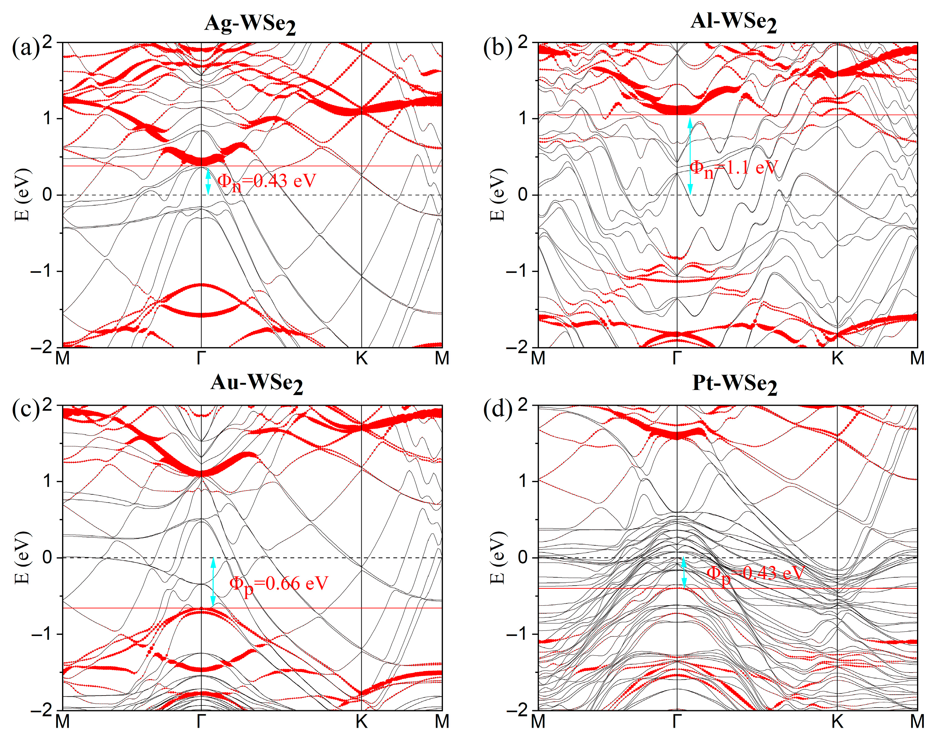
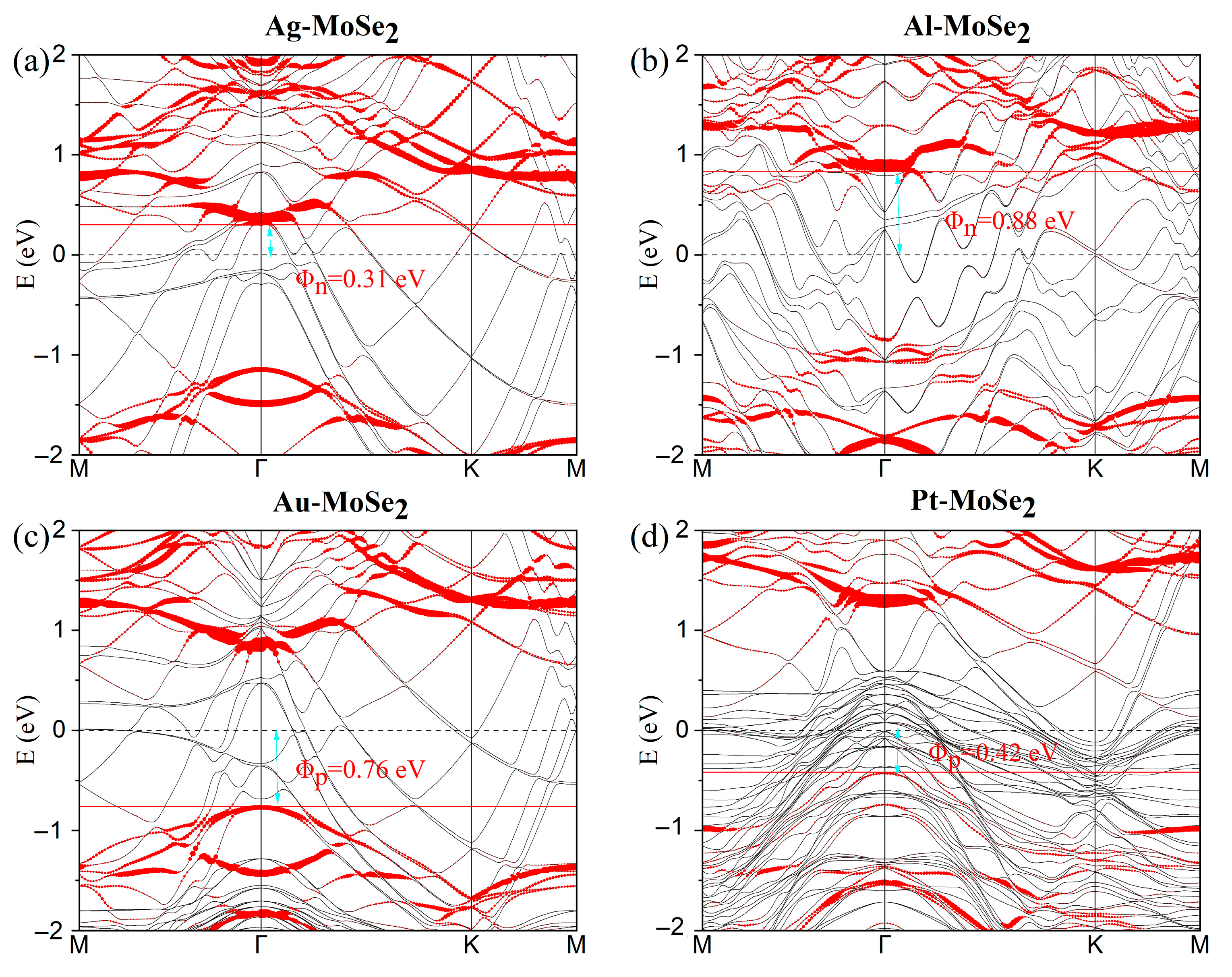
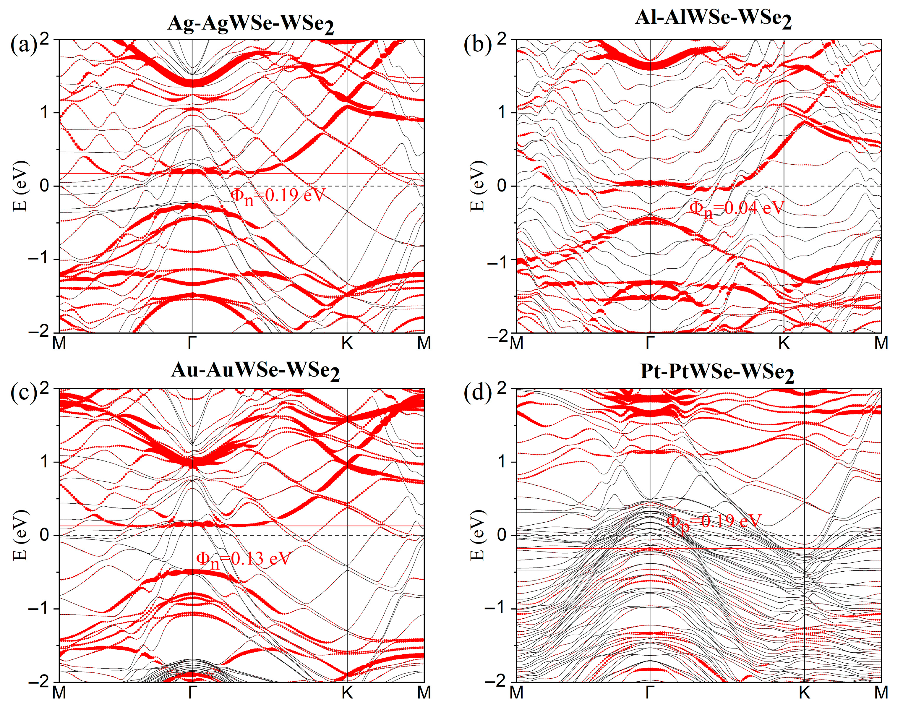
Figure 1. Interfacial geometries of contacts to ML WSe2/MoSe2. (a) Side and top views of Ag/Au (111)-WSe2/MoSe2 contacts. (b) Side and top views of WSe2/MoSe2 on Al/Pt (111) surfaces. (c) Side views of the metal–WSe2/MoSe2 contacts with a metal-doped mMoSe/mWSe buffer layer inserted.
Nanomaterials 15 01035 g001
Figure 2. (ad) Band structures of ML WSe2 in contact with several metals. The Fermi level is set to zero. The bands dominated by metal atoms and ML WSe2 are plotted using gray and red curves, respectively. The Schottky barrier is marked in red.
Nanomaterials 15 01035 g002
Figure 3. (ad) Band structures of ML MoSe2 in contact with several metals. The Fermi level is set to zero. The bands dominated by metal atoms and ML MoSe2 are plotted using gray and red lines, respectively. The Schottky barrier is marked in red.
Nanomaterials 15 01035 g003
Figure 4. (ad) Projected band structures of several metals in contact with ML WSe2 with inserted mWSe buffer layers. The Fermi level is set to zero. Red line: energy bands dominated by the WSe2 layer; gray line: band structures of metal–mWSe systems.
Nanomaterials 15 01035 g004
Figure 5. (ad) Projected band structures of several metals in contact with ML MoSe2 with inserted mMoSe buffer layers. The Fermi level is set to zero. Red line: energy bands dominated by the MoSe2 layer, gray line: band structures of metal–mMoSe systems.
Nanomaterials 15 01035 g005
Figure 6. Variation in the Schottky barrier height of electrons (Φn) with change in the work function for metal systems (a) in metal–MoSe2/WSe2 stacks and (b) in metal–mMoSe/mWSe–MoSe2/WSe2 stacks. The red and blue solid lines are fitted curves for metal systems in contact with WSe2 and MoSe2, respectively. Fermi-level depinning is seen after inserting a mMoSe/mWSe buffer layer, with pinning factors increased significantly.
Nanomaterials 15 01035 g006
Figure 7. Partial density of states (PDOS) of WSe2 after contact with (ad) metals and (eh) metallic mWSe surfaces for comparison. The Fermi level is at zero energy.
Nanomaterials 15 01035 g007
Figure 8. (a) Schematic diagram of a WSe2-MoSe2 heterostructure device. (b) Simplified band diagram for metal–MoSe2/WSe2 contacts, and the SBH and TB depend on the type of metal, which are related to the band hybridization degree. (c) Sketch of the band diagram for metal–mMoSe/mWSe-MoSe2/WSe2 stacks. The barrier height is reduced by suppressing the penetration of MIGSs.
Nanomaterials 15 01035 g008
Table 1. Calculated interfacial properties of WSe2 and MoSe2 on the metal electrodes. LM represents the lattice constant of the metals used in this article, with lattice mismatches in parentheses below. dZ is defined as the physical separation (the distance between the topmost metal atomic layer and the Se atoms in the z direction). Eb is the binding energy. W and WM are the calculated work functions for metal–WSe2/MoSe2 contacts and clean metal, respectively. The SBHs are extracted from the band calculation without (with) the insertion of a buffer layer (N electron Schottky barrier, and P hole Schottky barrier).
MetalLM
(Å)
WSe2/MoSe2
dZ
(Å)
Eb
(eV)
WM
(eV)
W
(eV)
SBH
(eV)
Ag5.778
(1.26/0.40%)
2.719/2.6830.284/0.3054.484.59/4.780.43 N/0.31 N
(0.19 N/0.00 N)
Al5.726
(0.36/0.49%)
2.912/2.7840.182/0.2054.114.37/4.621.1 N/0.88 N
(0.04 N/0.02 N)
Au5.767
(1.07/0.21%)
2.879/2.7800.252/0.2615.385.1/5.090.66 P/0.76 P
(0.13 N/0.03 N)
Pt5.549
(2.73/3.56%)
2.53/2.4880.318/0.3425.725.67/5.680.43 P/0.42 P
(0.19 P/0.29 P)
Disclaimer/Publisher’s Note: The statements, opinions and data contained in all publications are solely those of the individual author(s) and contributor(s) and not of MDPI and/or the editor(s). MDPI and/or the editor(s) disclaim responsibility for any injury to people or property resulting from any ideas, methods, instructions or products referred to in the content.

