Article

Multi-Bit Resistive Random-Access Memory Based on Two-Dimensional MoO3 Layers

1
Beijing Key Laboratory for Magneto-Photoelectrical Composite and Interface Science, School of Mathematics and Physics, University of Science and Technology Beijing, Beijing 100083, China
2
The State Key Laboratory for Advanced Metals and Materials, University of Science and Technology Beijing, Beijing 100083, China
*
Authors to whom correspondence should be addressed.
These authors contributed equally to this work.
Nanomaterials 2025, 15(13), 1033; https://doi.org/10.3390/nano15131033
Submission received: 30 April 2025 / Revised: 19 June 2025 / Accepted: 30 June 2025 / Published: 3 July 2025

Abstract

Two-dimensional (2D) material-based resistive random-access memory (RRAM) has emerged as a promising solution for neuromorphic computing and computing-in-memory architectures. Compared to conventional metal-oxide-based RRAM, the novel 2D material-based RRAM devices demonstrate lower power consumption, higher integration density, and reduced performance variability, benefiting from their atomic-scale thickness and ultra-flat surfaces. Remarkably, 2D layered metal oxides retain these advantages while preserving the merits of traditional metal oxides, including their low cost and high environmental stability. Through a multi-step dry transfer process, we fabricated a Pd-MoO3-Ag RRAM device featuring 2D α-MoO3 as the resistive switching layer, with Pd and Ag serving as inert and active electrodes, respectively. Resistive switching tests revealed an excellent operational stability, low write voltage (~0.5 V), high switching ratio (>106), and multi-bit storage capability (≥3 bits). Nevertheless, the device exhibited a limited retention time (~2000 s). To overcome this limitation, we developed a Gr-MoO3-Ag heterostructure by substituting the Pd electrode with graphene (Gr). This modification achieved a fivefold improvement in the retention time (>104 s). These findings demonstrate that by controlling the type and thickness of 2D materials and resistive switching layers, RRAM devices with both high On/Off ratios and long-term data retention may be developed.

1. Introduction

In recent years, artificial intelligence (AI), centered on machine learning (ML), has advanced rapidly, demonstrating its significant potential in fields such as autonomous driving, natural language processing, and image recognition [1]. This progress has imposed higher demands on data storage and logic operations. High-density, non-volatile memory has emerged as a key enabler for massive data processing in the era of big data. Among next-generation memory technologies, resistive random-access memory (RRAM) stands out as a highly promising candidate, attracting extensive research interest [2,3,4,5]. The basic structure of RRAM typically adopts a metal-insulator-metal (MIM) configuration. This simple architecture not only offers fabrication simplicity and compatibility with existing semiconductor processes but also exhibits excellent scalability for large-scale integration. Furthermore, RRAM’s multilevel cell (MLC) capability supports high-speed read/write operations [6,7], significantly enhancing its storage density [8,9] while reducing its power consumption [10,11]. These characteristics make RRAM particularly well-suited for big data and AI applications.
Conventional RRAM devices primarily utilize metal oxides (e.g., HfOx [12,13,14], TaOx [15,16,17], and TiOx [18,19,20]) as the resistive switching layer. Although metal-oxide-based memristors show great promise for neuromorphic computing and AI applications, their performance and integration levels still fall short of practical requirements. These devices typically suffer from high switching voltages, resulting in elevated power consumption. Moreover, as RRAM devices continue to scale down to achieve more complex functionalities, defects in the metal oxide layer become progressively difficult to control. Such local inhomogeneities and random defects critically impact the switching stability [21,22].
Recently, RRAM devices based on 2D layered materials have demonstrated significant potential in AI and in-memory computing applications [23]. Benefiting from their atomic-scale thickness and atomically smooth surfaces [24], these novel 2D material-based RRAM devices outperform their conventional metal-oxide-based counterparts by achieving lower power consumption, higher integration density, and reduced performance variability [25,26]. When 2D layered metal oxides are employed as the resistive switching layer, such devices not only retain the advantages of traditional metal-oxide RRAM (e.g., high environmental stability) but also enable new performance enhancements. Specifically, α-MoO3, with its wide bandgap (>3 eV), exhibits excellent insulating properties, making it an ideal candidate for resistive switching layers to ensure low off-state power consumption. In this study, α-MoO3 crystals were synthesized via physical vapor deposition (PVD) followed by mechanical exfoliation to obtain reproducible 2D α-MoO3 nanosheets. Through all-transfer, we fabricated Pd-MoO3-Ag devices demonstrating a low write voltage (~0.5 V), high switching ratio (>106), and multi-bit storage capability (≥3 bits). By replacing the palladium (Pd) electrode with 2D graphene (Gr) to construct Gr-MoO3-Ag devices, an extended retention time was achieved while maintaining the multi-bit storage capability. This work not only provides valuable insights into developing RRAM using 2D layered metal oxides as resistive switching layers but also establishes a universal methodology for characterizing resistive switching materials before and after the forming process.

2. Methods

2.1. Preparation of α-MoO3 Crystals and Thin Flakes

The α-MoO3 single crystals were synthesized via physical vapor deposition (PVD) under atmospheric pressure. The synthesis process involved the following: (1) placing a quartz boat containing MoO3 powder (Aladdin, 99.95%) at the central heating zone of a tube furnace, with the other quartz boat positioned at the cold zone (25 cm apart) to collect the synthesized crystals; (2) introducing an oxygen carrier gas at a constant flow of 50 sccm to transport the vaporized MoO3; (3) heating the furnace to 750 °C at a rate of 20 °C/min and maintaining for 60 min. After growth, the heating was stopped, and the furnace was immediately opened for rapid cooling, and the bulk α-MoO3 crystals were collected. For thin flake preparation, multilayer α-MoO3 flakes were mechanically exfoliated from the bulk crystals onto polydimethylsiloxane (PDMS) substrates using scotch tape for subsequent dry transfer processes.

2.2. Fabrication of Pd-MoO3-Ag Devices

First, few-layer α-MoO3 flakes were mechanically exfoliated onto a PDMS substrate, then dry transferred onto a SiO2/Si wafer with pre-patterned Pd electrodes (50 nm thickness, deposited by thermal evaporation) to establish the Pd-MoO3 interfacial contact. The few-layer α-MoO3 flakes were then treated with air plasma for 15 s and covered with Ag/Au electrodes using the PDMS-mediated dry transfer. Finally, the Pd-MoO3-Ag device was annealed at 200 °C for 1 h in a vacuum to optimize the interfacial contacts.

2.3. Fabrication of Gr-MoO3-Ag Devices

First, few-layer graphene was mechanically exfoliated onto a PDMS substrate, followed by being dry transferred onto a SiO2/Si wafer with pre-patterned, 50 nm thick Pd electrodes to establish the graphene-Pd contact at one end to prevent direct contact between the probe and the graphene and to avoid damaging the graphene. Then, few-layer α-MoO3 flakes were mechanically exfoliated onto another PDMS substrate and, subsequently, dry transferred onto the surface of the graphene on the SiO2/Si wafer, creating an α-MoO3-graphene contact at the other end of the graphene. The upper surface of the few-layer α-MoO3 flake was treated with air plasma for 15 s. Then, Ag/Au electrodes were dry transferred onto the α-MoO3 surface by PDMS mediation. Finally, the Gr-MoO3-Ag device was annealed at 200 °C for 1 h in a vacuum to optimize the interfacial contacts.

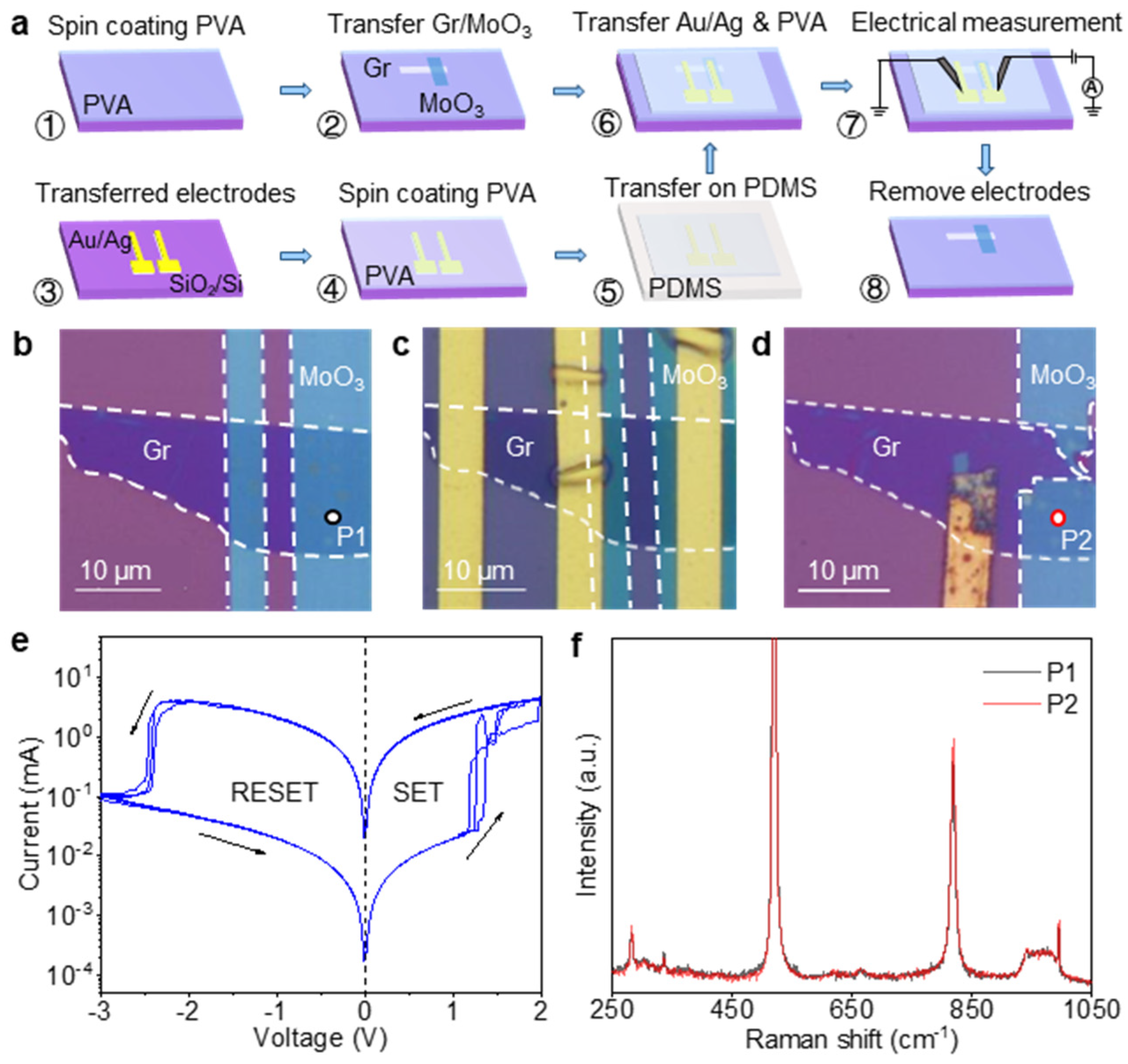
2.4. Fabrication of Detachable Devices

The fabrication process of the detachable device involved the following: first, a polyvinyl alcohol (PVA, average polymerization degree-2688) layer was spin-coated onto a SiO2/Si substrate, followed by the dry transfer assembly of a Gr-MoO3 heterostructure, where multilayer graphene served as the bottom electrode under the MoO3 flake. Secondly, Ag/Au electrodes were transferred onto another SiO2/Si substrate and spin-coated with another kind of PVA (average polymerization degree-0588). The PVA-0588 layer was precisely cut off around the electrodes, and a PDMS substrate was used to tear off the cut PVA and the Ag/Au electrodes together. Finally, we aligned and transferred the Ag/Au electrodes embedded in the PVA onto the pre-formed Gr-MoO3 heterostructure to obtain the Gr-MoO3-Ag stacked device.
Thin films were fabricated using PVAs with average polymerization degrees of 2688 and 0588. DP-2688: 8 wt% of solution was pipetted onto substrates, followed by two-step spin-coating (500 rpm for 5 s and 8000 rpm for 60 s). DP-0588: 5 wt% of solution was pipetted and spin-coated identically, except for the 4500 rpm for the 60 s for high-speed step. All the films were cured at 70 °C for 60 s on a hot plate.

2.5. Characterizations

X-ray diffraction (XRD) measurements were conducted on an X-ray diffractometer (Model: Rigaku SmartLab (3); Beijing, China) using Cu Kα radiation (λ = 0.154056 nm) under the ambient conditions. The X-ray photoelectron spectroscopy (XPS) analysis was carried out on an X-ray energy spectrometer (Model: Thermo Scientific K-Alpha; Beijing, China) employing monochromatic Al Kα X-ray with an operating spot of 400 μm in diameter. The binding energy was calibrated to the adventitious carbon C 1s peak at 284.80 eV. Raman spectroscopy was performed at room temperature using a confocal Raman system (Model: Horiba Jobin Yvon HR800; Beijing, China) with a 532 nm excitation laser focused through a 100×/N.A. 0.90 objective to achieve a spot size of approximately 1.5 μm, providing a spectral resolution of 1.5 cm−1. The surface topography and the thickness of the samples were characterized by atomic force microscopy (Model: Bruker Multimode 8; Beijing, China). A focused ion beam (Model: Thermo Scientific Helios 5 UX DualBeam; Beijing, China) was utilized to prepare the cross-sectional sample of the Pd-MoO3-Ag device. Transmission electron microscopy (Model: Titan ETEM G2; Beijing, China) was used to characterize the microstructure of the α-MoO3 flake and the Pd-MoO3-Ag heterostructure.

3. Results and Discussion

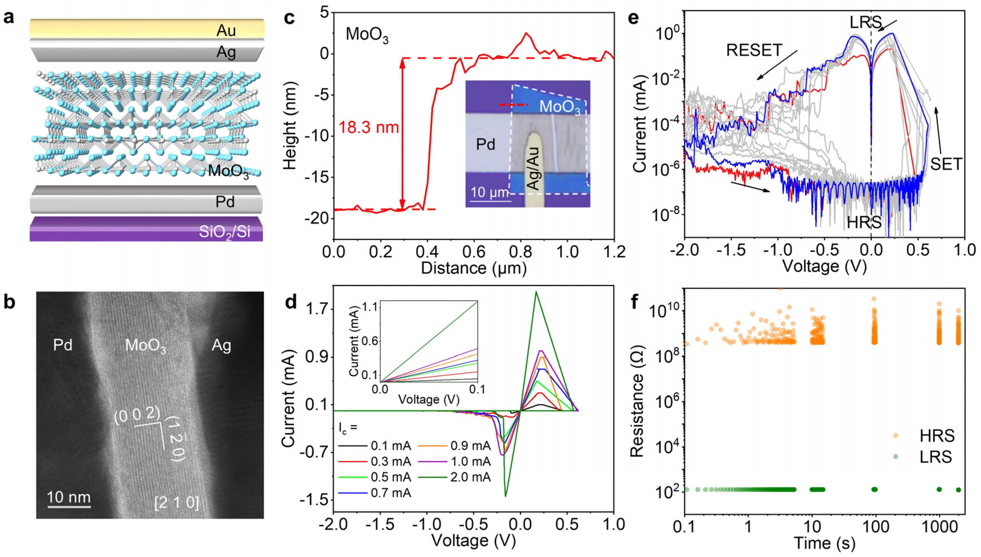
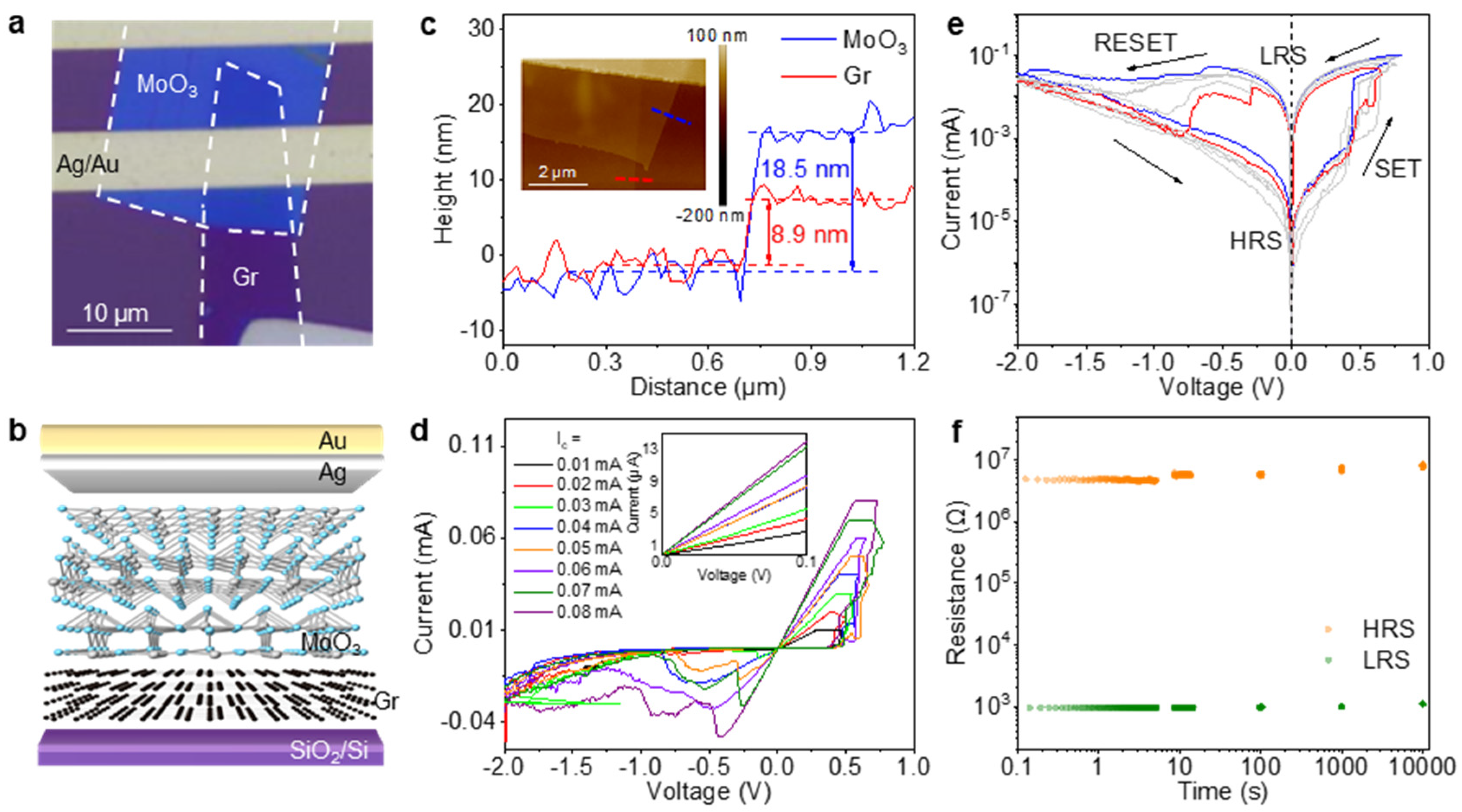
3.1. Characterizations of α-MoO3

α-MoO3 is a layered oxide composed of double-layered MoO6 octahedra parallel to the (0 1 0) plane, with adjacent layers bonded by relatively weak van der Waals forces. In the MoO6 octahedron, each Mo atom is surrounded by six oxygen atoms, and these octahedra connect through shared vertices and edges to form a 2D layered network [27]. X-ray diffraction (XRD) was used to characterize the crystallinity of bulk α-MoO3 crystals obtained via the PVD method. As shown in Figure 1a, distinct diffraction peaks appear at 12.8°, 25.7°, 39.0°, 52.8°, and 67.6°, corresponding to the (0 2 0), (0 4 0), (0 6 0), (0 8 0), and (0 10 0) planes of α-MoO3 (PDF#35-0609), respectively. The observation of only (0 k 0) peaks in the XRD pattern indicates that the [0 1 0] direction of the α-MoO3 crystal is perpendicular to the SiO2/Si substrate, while the α-MoO3 flakes are parallel to it. The diffraction results correspond to the space group Pbnm with lattice parameters of a = 0.3962 nm, b = 1.3855 nm, and c = 0.3699 nm. The XRD result reveals that the MoO3 bulk that was grown by PVD is a single crystal.
X-ray photoelectron spectroscopy (XPS) was employed to characterize the elemental composition and chemical states of the α-MoO3 flakes. The binding energy scale was calibrated by setting the C 1 s peak to 284.80 eV. As shown in Figure 1b, the characteristic doublet peaks of Mo 3d3/2 and Mo 3d5/2 in α-MoO3 were detected at 236.4 and 233.2 eV, respectively, which can be attributed to the Mo6+ oxidation state of the α-MoO3 phase [28,29,30].
To investigate the microstructure of α-MoO3, transmission electron microscopy (TEM) and high-resolution TEM (HRTEM) were utilized. Figure 1c presents a low-magnification TEM image of a typical few-layer α-MoO3 flake. The inset in Figure 1c displays the selected-area electron diffraction (SAED) pattern obtained from the region marked by the white, dashed circle, where the diffraction spots corresponding to the (1 0 1) and (0 0 2) planes of α-MoO3 are clearly indexed. These results indicate the [0 1 0] zone axis for α-MoO3, consistent with the Pbnm space group of α-MoO3. Figure 1d shows a representative HRTEM image of α-MoO3, revealing two sets of perpendicular lattice fringes with measured spacings of 0.39 and 0.37 nm, which match the interplanar distances of the (1 0 0) and (0 0 1) planes of α-MoO3 [31]. The inset in Figure 1d reveals a simulated HRTEM image along the [0 1 0] zone axis, demonstrating excellent agreement with the experimental image, thereby providing further confirmation of the α-MoO3 phase.
Raman spectroscopy serves as a crucial technique for characterizing crystal structures and phonon vibration modes of materials. The Raman spectrum of α-MoO3 exhibits multiple characteristic peaks in the range of 250~1000 cm−1, primarily associated with the vibration modes of Mo-O bonds in its crystal structure. As shown in Figure 1e, distinct Raman peaks originate from the different vibration modes of the Mo-O-Mo bridging bonds and two types of terminal oxygen (Mo=O). For the terminal oxygen vibrations, the wagging mode appears at 283 cm−1 (B1g, B3g), the shearing mode at 365 cm−1 (Ag), the symmetric stretching mode at 818 cm−1 (Ag, B2g), and the asymmetric one at 995 cm−1 (Ag, B2g). For Mo-O-Mo bridging bond vibrations, the bending mode appears at 337 cm−1 (Ag, B2g) and the stretching one at 665 cm−1 (B1g, B3g) [32]. We systematically investigated the evolution of the Raman spectra of α-MoO3 flakes before and after thermal or surface treatments (Figure 1e). While the peak positions remained nearly unchanged, significant variations in the peak intensity and the full-width-at-half-maximum (FWHM) were observed. Detailed data can be found in Tables S1 and S2 in the Supporting Information. Figure 1f shows that the peak intensity of all the Raman modes is enhanced after annealing in air at 200 °C for 30 min, while a subsequent air plasma treatment for 120 s can reduce the peak intensity, compared with the untreated counterpart. As shown in Figure 1g, the FWHM values of five characteristic Raman peaks (excluding the 818 cm−1 peak) decreased after annealing but increased beyond the pre-treatment levels following plasma treatment. It is noted that the change in the FWHM values of the Raman peak at 818 cm−1 shows an opposite trend (highlighted by the red, dashed frame in Figure 1g): its FWHM increased after heating but decreased after plasma treatment, though remaining larger than the initial value. In a Raman spectrum, a perfect crystalline lattice produces sharp vibration peaks with high intensity and small FWHM values. Defects (e.g., vacancies, dislocations) or amorphous phases in the materials can give rise to complex phonon modes, frequency shifts, wider peak widths, and weaker intensities. Our analysis suggests that thermal annealing in air helps repair defects in α-MoO3, while plasma treatment introduces additional defects. The anomalous behavior of the 818 cm−1 peak may stem from the surface reactions with atmospheric O2 during heating, which increases the concentration of terminal oxygen in the Mo=O with the enhanced peak intensity. In the subsequent cooling process, airborne molecules may be adsorbed, which perturb the symmetric stretching vibrations of terminal oxygen, thus resulting in larger FWHM values.
The characterization and analysis in Figure 1 demonstrate that the α-MoO3 crystals prepared by the PVD method exhibit good overall crystallinity while containing localized oxygen vacancies or other defects. Thermal annealing in air can reduce defect concentration, thereby enhancing the Raman peak intensities of both Mo-O-Mo and Mo=O bonds. Conversely, the plasma treatment introduced additional defects into the α-MoO3. This systematic investigation on different treatments provides a simple, yet effective, approach for the controllable modulation of oxygen vacancies or defects in the resistive switching layer of RRAM devices.

3.2. Fabrication and Resistive Switching Performance of RRAM

The Pd-MoO3-Ag device was fabricated with a vertical architecture on a SiO2/Si substrate containing pre-patterned Pd electrodes. Figure 2a shows its cross-sectional schematic. Palladium was selected as the inert electrode material due to its excellent stability. Pd electrodes with a thickness of 50 nm were deposited via electron-beam evaporation. The α-MoO3 resistive switching layer was prepared by mechanically exfoliating PVD-grown α-MoO3 crystals, followed by a PDMS-mediated dry transfer onto the Pd electrode. Atomic force microscopy (AFM) measurements determined the α-MoO3 layer thickness to be approximately 18.3 nm (Figure 2c). The α-MoO3 surface underwent a 15 s air plasma treatment to introduce controlled defects intentionally. Finally, a patterned Ag/Au electrode was dry transferred onto the α-MoO3 flake, with subsequent 1 h vacuum annealing at 200 °C to optimize the electrode interface contact. A high-resolution transmission electron microscopy (HRTEM) analysis of the focused ion beam (FIB)-prepared device cross-section revealed well-defined van der Waals interfaces in the pristine device before the electrical measurements (Figure 2b). The HRTEM image distinctly exhibits lattice fringes in the resistive switching layer, consistent with single-crystalline α-MoO3 oriented along the [2 1 0] zone axis. Figure S1b,c display the fast Fourier transform pattern of the cross-section and the simulated electron diffraction pattern along the [2 1 0] zone axis.
Notably, our developed Pd-MoO3-Ag devices demonstrate multilevel storage capability through the controlled regulation of the compliance current (Ic). In RRAM devices, the SET process typically involves the formation of conductive filaments. A failure to set a compliance current may induce excessive current flow, promoting the overgrowth of the conductive filaments and potentially causing irreversible device breakdown. The imposition of a compliance current enforces a maximum current limit during SET operation, which safeguards the device from damage. Moreover, varying compliance currents directly modulate the growth extent of conductive filaments, consequently determining the resultant resistance value. As shown in Figure 2d, distinct intermediate resistive states emerge in the current-voltage (I-V) characteristics under different Ic values. Figure S2 further reveals that under identical voltage pulse stimulation (1.2 s duration, 1 V amplitude), varying the Ic settings generates discrete current values at a fixed read voltage of 0.1 V, showing a monotonic increase in the read current with Ic. Figure 2d shows seven distinct current values corresponding to seven Ic settings at a 0.1 V bias, demonstrating a clear positive correlation between the current magnitude and the Ic. Combined with the high-resistance state (HRS), the device achieves at least eight non-volatile resistive states, enabling a reliable 3-bit storage capacity. This controlled multilevel switching behavior highlights the device’s exceptional multi-bit storage capability through precise compliance current engineering.
The SET operation is the process of switching the RRAM device from a high-resistance state to a low-resistance state. The RESET operation is the process of switching the RRAM device back from a low-resistance state to a high-resistance state.
The resistive switching characteristics of the Pd-MoO3-Ag device under the controlled Ic are systematically investigated in Figure 2e. Cyclic I-V measurements demonstrate a highly reproducible switching behavior across different Ic conditions, confirming a good operational stability. In our measurement, a scanning voltage sequence of 0 → 1.0 → 0 → −2.0 → 0 V is used. Because of the limitation of our testing equipment, once the current reaches the compliance value (Ic), the voltage is controlled to regulate the current, thus preventing any further increase in the actual value of the voltage. The device achieves a remarkably low write voltage of ~0.5 V, providing two key advantages: (1) a reduced dynamic power consumption (PV2), particularly crucial for high-density memory and low-power electronics; (2) a low operational voltage, significantly suppressing Joule heating and mitigating thermally induced performance degradation. As the scaling of the semiconductor technology nodes and the reduction of the core operating voltages continue, such low-voltage RRAM devices demonstrate direct compatibility with advanced process nodes, thereby eliminating the need for additional voltage conversion circuitry.
The device exhibits an erase voltage of −0.7 to −2.0 V, with this modest magnitude providing dual benefits, namely reduced operational energy consumption and suppressed material fatigue (like electrode material diffusion), enhancing cycling endurance. The device exhibits an exceptional switching ratio exceeding 106. This enhanced resistance contrast enables two critical operational advantages: (1) improved noise immunity through robust differentiation between HRS and LRS, significantly enhancing read reliability; (2) a reduced read voltage requirement (≤0.1 V) that enables precise state discrimination while simultaneously reducing power consumption. Figure S3 shows the resistance variation in the HRS and the LRS as a function of the cycle number.
Retention time, a critical performance metric for non-volatile RRAM, quantifies the duration during which stored data can be reliably preserved without power. To evaluate this parameter, we applied a programming voltage pulse (1 s duration, 1 V amplitude) followed by read operations at 0.1 V at progressive time intervals (0, 10, 100, 1000, and 2000 s). As shown in Figure 2f, the Pd-MoO3-Ag device demonstrates a retention capability exceeding 2000 s, confirming stable non-volatile storage characteristics, an essential requirement in memory applications. Notably, in the HRS, the current becomes extremely low, approaching the measurement limit of our instrumentation, resulting in inherent signal fluctuations. This instrumentation-limited current measurement (Figure 2e) consequently induces calculated resistance variations in the HRS, as shown in Figure 2f.
The Pd-MoO3-Ag device with a 2D MoO3 resistive switching layer demonstrated an excellent stability, a low write voltage, a high switching ratio, and a multi-bit storage capability in previous tests. However, its 2000 s retention time posed limitations for practical applications. Two-dimensional layered materials allow the intercalation of external particles between adjacent layers. When used as electrodes, they can modulate the ion migration dynamics. To enhance the retention characteristics, we developed a Gr-MoO3-Ag device through the replacement of the Pd bottom electrode with 2D graphene (Gr) via a similar dry transfer process. The device architecture is illustrated in Figure 3a (top view) and Figure 3b (side view). Graphene exhibits exceptional electrical conductivity, thermal conductivity, and mechanical flexibility [33], while its atomically smooth surface effectively reduces the defect concentration at the MoO3 interface. This synergistic combination significantly improves the reliability and stability of the RRAM device.
Figure 3a,b show the optical image and the structural schematics of the Gr-MoO3-Ag device. The AFM image in the inset of Figure 3c displays exceptionally smooth material surfaces, where red and blue profile lines correspond to step heights of 8.9 nm (Gr) and 18.5 nm (α-MoO3). To compare with the cycling test data of the Pd-electrode device, the same scanning voltage sequence of 0 → 1.0 → 0 → −2.0 → 0 V was applied to this device. As illustrated in Figure 3e, a complete reset can be achieved under a smaller Ic, which is confirmed by the overlapping of the I-V curves near −2.0 V (red curve). Under a higher Ic, the increased accumulation of conductive filaments in the MoO3 layer requires larger negative voltages to successfully finish the RESET operation. Consequently, within the same voltage range, the complete reset cannot be accomplished under a higher Ic. Figure 3d demonstrates I-V characteristics with multiple intermediate resistive states under different Ics. The inset of Figure 3d confirms that, including the HRS, the Gr-MoO3-Ag device achieves eight distinct resistive states through Ic modulation, enabling a reliable 3-bit storage capability.
Figure 3e illustrates the resistive switching behavior of the Gr-MoO3-Ag device. Cyclic I-V measurements under different Ics reveal highly superimposable hysteresis curves, indicating a good cycling stability. Key operational parameters include a write voltage of ~0.5 V, a switching ratio of ~5 × 10³, and an erase voltage range of −1.0 to −2.0 V. As shown in Figure 3f, the Gr-MoO3-Ag device exhibits a retention time exceeding 104 s. While both the Gr-MoO3-Ag and the Pd-MoO3-Ag devices enable multi-bit storage capabilities, the comparative analysis demonstrates distinct performance trade-offs: the Pd-MoO3-Ag device displayed superior resistive switching characteristics with a higher switching ratio (106 vs. 5 × 10³) and higher resistance (109 vs. 5 × 10⁶ Ω). The Pd-electrode devices showed a SET voltage of approximately 0.5 V and a RESET voltage ranging from −0.7 to −2.0 V, while the Gr-electrode devices exhibited a similar SET voltage of ~0.5 V but required a slightly higher RESET voltage window of −1.0 to −2.0 V. Conversely, the Gr-MoO3-Ag device achieves markedly extended retention characteristics, maintaining the data integrity for five times longer than the Pd-based device (10,000 vs. 2000 s at room temperature).

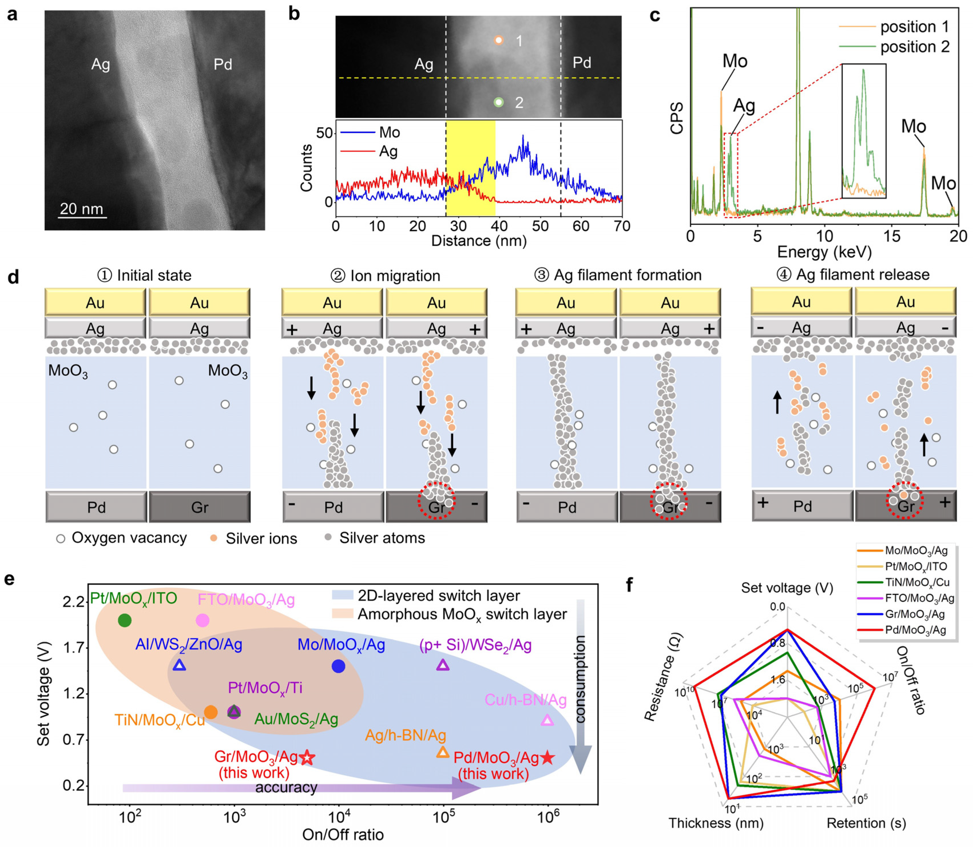
3.3. Analysis of Device Operating Mechanisms

To compare the property of the α-MoO3 resistive switching layer in RRAM devices before and after electrical I-V cycling tests, we adopted a reconfigurable device fabrication method [34], with the procedures illustrated in Figure 4a. The procedures include the following steps: (1) Spin-coating a polyvinyl alcohol (PVA, average polymerization degree, 2688) layer on a SiO2/Si substrate. (2) Dry transferring it to construct a Gr-MoO3 heterostructure on the PVA layer (Figure 4a②). In this configuration, multilayer graphene serves as the bottom electrode beneath the MoO3 flake, as shown in the optical image (Figure 4b). (3) Performing the initial Raman characterization of the MoO3 layer from P1, as marked in Figure 4b. The result is shown by the black curve in Figure 4f. Subsequent steps involved the following: (4) Transferring pre-patterned Ag/Au electrodes onto another SiO2/Si substrate (Figure 4a③). (5) Spin-coating another kind of PVA layer (average polymerization degree, 0588) and patterning it around the electrodes. (6) Delaminating the patterned PVA layer with embedded Ag/Au electrodes using PDMS (Figure 4a⑤). (7) Transferring this stack onto the pre-formed Gr-MoO3 heterostructure to complete the assembly of the Gr-MoO3-Ag device (Figure 4a⑥), with the final structure shown in Figure 4c. For electrical measurements, probes directly penetrate the PDMS thin layer to contact the Ag/Au electrodes (Figure 4a⑦). In practice, the leftmost and rightmost metal electrodes were connected to graphene and MoO3, respectively. (8) After testing, the PVA (average polymerization degree, 0588) layer and the Ag/Au electrodes were delaminated with adhesive tape, revealing the post-cycling MoO3 layer, as illustrated in Figure 4a⑧.
In the experiment, we used a scanning voltage sequence of 0 → 2.0 → 0→ −3.0 → 0 V. Our resistive switching characterization on the Gr-MoO3-Ag device (Figure 4e) revealed a distinct switching behavior with a write voltage of ~1.3 V and a switching ratio of > 102. To preserve the integrity of the PVA, both the annealing and the plasma treatment were intentionally omitted during device fabrication, resulting in enlarged interfacial gaps between the MoO3 and the electrodes with a reduced surface defect density in MoO3. These structural characteristics collectively affect the device performance: the expanded gaps decelerate Ag ion migration, while the sparse defects confine the growth of conductive filaments to specific sites, leading to concentrated filament accumulation at these limited defect locations that elevates the off-state current (Ioff) and diminishes the switching ratio. Crucially, this spatially constrained growth of the conductive filaments coupled with the moderated switching ratio synergistically enhances the overall stability of the resistive switching operation.
Following the switching characterization, we independently executed a SET operation through a 0 to 2.0 V voltage sweeping to stabilize the device in its LRS prior to mechanical delamination. The PVA (degree of polymerization, 0588) layer and the Ag/Au electrodes were subsequently exfoliated using adhesive tape, thereby exposing the post-cycling MoO3 layer. The optical image in Figure 4d shows the residual Ag/Au electrode and the partial loss of the MoO3 layer after electrode stripping. Subsequent Raman measurements at the identical location (P2 marked in Figure 4d) demonstrated a remarkable spectral consistency between the post-cycling (red spectrum, Figure 4f) and the pre-test (black spectrum) conditions, with both the peak positions and the relative intensities showing negligible variation. This indicates the preservation of the α-MoO3 crystalline integrity following multiple SET/RESET cycles under mild operating conditions. The exceptional structural stability of the 2D α-MoO3 not only ensures enhanced device endurance and operational reliability but also positions this material as a superior alternative to conventional oxide-based, non-volatile memory. Figure S4 shows the invariance in both the peak positions and the intensities of the Raman spectra of Gr before and after performance testing.
The working principle of RRAM is primarily based on two physical mechanisms: the valence change mechanism (VCM) and the electrochemical metallization mechanism (ECM) [3,25]. In our experiment, a silver electrode was employed as the active electrode to achieve resistance state switching through the formation and dissolution of conductive channels via silver ion migration. A Pd-MoO3-Au device without an active electrode was also prepared as a counterpart. Figure S5 reveals that the intrinsic α-MoO3 without the Ag electrode exhibits no resistive switching behavior. Therefore, the formation and dissolution of conductive channels of silver ions is indispensable in the MoO3-based RRAM. This mechanism is supported by Figure 5a, which shows significant structural changes in the MoO3 resistive switching layer after >100 I-V cycles and retention tests compared to its initial crystalline lattice (Figure 2b). The contrast variations observed in the MoO3 layer indicate material modifications during operation. Furthermore, the line scanning of the elemental distribution along the yellow, dashed line in the top panel of Figure 5b revealed the simultaneous detection of Ag and Mo elements within the 27~39 nm range (Figure 5b, bottom panel), confirming the incorporation of Ag into the switching layer. Additionally, the point-scan EDS analysis at positions 1 and 2, marked in Figure 5b (top panel), demonstrated the presence of Ag only at position 2. These results collectively indicate that the silver injection into the MoO3 layer occurs through random and localized penetration. This conclusion is further supported by the contrast variations observed in Figure 5b.
The operational mechanisms during the SET and RESET processes in both the Pd-MoO3-Ag and the Gr-MoO3-Ag RRAM devices, where Pd or graphene serves as the bottom electrode and Ag as the top electrode, are schematically illustrated in Figure 5d. The process begins with the inherent presence of low-concentration oxygen vacancies and other defects in the α-MoO3 resistive switching layer, which unavoidably form during oxide preparation (Figure 5d①). In the SET process, as shown in Figure 5d②, when a positive voltage is applied to the active electrode (with the inert electrode negatively biased), Ag atoms at the interface undergo electrochemical oxidation to form Ag ions. These Ag ions then migrate through the resistive switching layer toward the inert electrode under the influence of the electric field. Upon reaching the inert electrode surface, the Ag ions gain electrons and are reduced to Ag atoms. The accumulation of Ag atoms under the bias voltage progressively forms a conductive filament that bridges the two electrodes. Once the conductive filament is fully established, the device switches to the LRS (Figure 5d③). In the RESET process, as shown in Figure 5d④, a positive voltage is applied to the inert electrode (with the active electrode negatively biased), and the Ag atoms in the conductive filament are oxidized into Ag ions. These Ag ions subsequently migrate toward the active electrode, causing the conductive filament to gradually dissolve. When the filament is completely ruptured, the conductive pathway is eliminated, and the device returns to the HRS.
The operational principles of the Pd-MoO3-Ag and the Gr-MoO3-Ag devices differ subtly. Owing to the unique layered structure of van der Waals materials, their interlayers can accommodate the intercalation of external particles (e.g., atoms, molecules, or ions). When graphene acts as the electrode, silver ions may intercalate into the surface layers of multilayer graphene [35], where they are subsequently reduced to silver atoms, as illustrated in Figure 5d②,③. This intercalation process could hinder the migration rate of silver ions, thereby influencing the accumulation of silver atoms in the resistive switching layer. Consequently, as shown in Figure 3e, the Gr-MoO3-Ag device exhibits a significantly increased off-state current due to the accumulation of silver atoms. Because of this, the mechanism can promote the conductive filament’s stability, leading to improved retention characteristics.
As shown in Figure 5e, a comparative analysis of the resistive switching (RS) devices employing either molybdenum oxides or 2D layered materials as resistive switching layers [36,37,38,39,40,41,42,43,44,45] reveals that our devices achieve superior performances in both the write voltage and the On/Off ratio. Furthermore, Figure 5f specifically benchmarks molybdenum-oxide-based RS devices across five key parameters—the switching layer thickness, resistance in HRS, write voltage, On/Off ratio, and retention time [36,37,38,40]—demonstrating four significant advantages of our devices: thinner switching layers (enabling higher integration density), higher HRS resistance, a lower write voltage (reducing the dynamic power consumption following PV2), and a higher On/Off ratio (enhancing read reliability). These combined improvements (detailed data are presented in Tables S3 and S4) contribute to a low-power operation with minimal storage errors. This comprehensive performance profile underscores their strong potential for application in next-generation RRAM technology. Compared with recently reported multilevel RRAM devices (Table S5 and Figure S6) [46,47,48,49], our fabricated devices demonstrate a comparable multilevel storage capability while exhibiting significantly lower write voltages.

4. Conclusions

In summary, we successfully synthesized bulk α-MoO3 crystals via the PVD method and obtained 2D α-MoO3 flakes through mechanical exfoliation. Comprehensive characterization using XRD, XPS, Raman spectroscopy, and TEM confirmed the high crystalline quality and the structural integrity of the α-MoO3. Subsequently, through a multi-step dry transfer process, we fabricated Pd-MoO3-Ag RRAM devices employing 2D α-MoO3 as the resistive switching layer, with Pd and Ag serving as inert and active electrodes, respectively. The devices demonstrated excellent performance metrics, including remarkable stability, a low write voltage (~0.5 V), a high switching ratio (>106), and a multilevel storage capability (≥3 bits). However, the retention time of ~2000 s posed practical limitations. To address this issue, we developed Gr-MoO3-Ag devices by replacing the Pd electrode with multilayer Gr. Although these devices exhibited a slightly compromised write voltage and switching ratio compared to the Pd-MoO3-Ag counterparts, the unique layered structure of Gr enabled the intercalation of Ag atoms/ions, resulting in a fivefold improvement in the retention time (>104 s). This work establishes that the strategic selection and structural optimization of electrode materials (considering their type, thickness, and interfacial properties), combined with appropriate resistive switching layers, can obtain RRAM devices capable of simultaneously achieving both high switching ratios and extended retention times.

Supplementary Materials

The following supporting information can be downloaded at https://www.mdpi.com/article/10.3390/nano15131033/s1.

Author Contributions

Conceptualization, K.L. and W.J.; Methodology, K.L., W.J., L.Z., Y.Z. (Yinkang Zhou), M.H., Y.G., Y.Z. (Yiyuan Zhang) and Y.Q.; Software, Y.Z. (Yinkang Zhou) and Y.Z. (Yiyuan Zhang); Formal analysis, K.L. and Y.S.; Investigation, K.L., W.J., M.H. and Y.G.; Resources, Y.Q., R.W. and Y.S.; Data curation, W.J.; Writing—original draft, K.L.; Writing—review & editing, W.J., L.Z., R.W. and Y.S.; Supervision, Y.S.; Project administration, R.W.; Funding acquisition, R.W. and Y.S. All authors have read and agreed to the published version of the manuscript.

Funding

This research was funded by the National Natural Science Foundation of China (Nos. 12374169, 12034002).

Data Availability Statement

The original contributions presented in this study are included in the article/Supplementary Material. Further inquiries can be directed to the corresponding authors.

Acknowledgments

Wengui Jiang and Yinghui Sun gratefully acknowledge Kai Liu from the School of Materials Science and Engineering at Tsinghua University for providing access to the AFM instrument.

Conflicts of Interest

The authors declare no conflicts of interest.

References

  1. Yadav, D. Machine learning: Trends, perspective, and prospects. Science 2020, 349, 255–260. [Google Scholar]
  2. Pan, F.; Gao, S.; Chen, C.; Song, C.; Zeng, F. Recent progress in resistive random access memories: Materials, switching mechanisms, and performance. Mater. Sci. Eng. R Rep. 2014, 83, 1–59. [Google Scholar] [CrossRef]
  3. Menzel, S.; Böttger, U.; Wimmer, M.; Salinga, M. Physics of the switching kinetics in resistive memories. Adv. Funct. Mater. 2015, 25, 6306–6325. [Google Scholar] [CrossRef]
  4. Wu, H.; Wang, X.H.; Gao, B.; Deng, N.; Lu, Z.; Haukness, B.; Bronner, G.; Qian, H. Resistive random access memory for future information processing system. Proc. IEEE 2017, 105, 1770–1789. [Google Scholar] [CrossRef]
  5. Chang, T.C.; Chang, K.C.; Tsai, T.M.; Chu, T.J.; Sze, S.M. Resistance random access memory. Mater. Today 2016, 19, 254–264. [Google Scholar] [CrossRef]
  6. Chen, Z.; Huang, W.; Zhao, W.; Hou, C.; Ma, C.; Liu, C.; Sun, H.; Yin, Y.; Li, X. Ultrafast multilevel switching in Au/YIG/n-Si RRAM. Adv. Electron. Mater. 2019, 5, 1800418. [Google Scholar] [CrossRef]
  7. Cario, L.; Vaju, C.; Corraze, B.; Guiot, V.; Janod, E. Electric-field-induced resistive switching in a family of Mott insulators: Towards a new class of RRAM memories. Adv. Mater. 2010, 22, 5193–5197. [Google Scholar] [CrossRef]
  8. Wu, M.C.; Ting, Y.H.; Chen, J.Y.; Wu, W.W. Low power consumption nanofilamentary ECM and VCM cells in a single sidewall of high-density VRRAM arrays. Adv. Sci. 2019, 6, 1902363. [Google Scholar] [CrossRef]
  9. Xie, M.; Jia, Y.; Nie, C.; Liu, Z.; Tang, A.; Fan, S.; Liang, X.; Jiang, L.; He, Z.; Yang, R. Monolithic 3D integration of 2D transistors and vertical RRAMs in 1T-4R structure for high-density memory. Nat. Commun. 2023, 14, 5952. [Google Scholar] [CrossRef]
  10. Jian, J.; Dong, P.; Jian, Z.; Zhao, T.; Miao, C.; Chang, H.; Chen, J.; Chen, Y.-F.; Feng, H.; Sorli, B. Ultralow-power RRAM with a high switching ratio based on the large van der Waals interstice radius of TMDs. ACS Nano 2022, 16, 20445–20456. [Google Scholar] [CrossRef]
  11. Han, S.W.; Shin, S.; Lee, C.T.; Shin, M.W. Laser-modulated formation of conduction path for the achievement of ultra-low switching voltage in resistive random-access memory (RRAM). Nano Energy 2023, 117, 108886. [Google Scholar] [CrossRef]
  12. Xie, W.; Bai, J.; Li, Y.; Qin, F.; Wang, D. Interface characteristic and performance optimization mechanism for HfOx-based RRAM devices. Appl. Surf. Sci. 2025, 680, 161291. [Google Scholar] [CrossRef]
  13. Ranjan, A.; Xu, H.; Wang, C.; Molina, J.; Wu, X.; Zhang, H.; Sun, L.; Chu, J.; Pey, K.L. Probing resistive switching in HfO2/Al2O3 bilayer oxides using in-situ transmission electron microscopy. Appl. Mater. Today 2023, 31, 101739. [Google Scholar] [CrossRef]
  14. Yeh, K.; Shih, P.; Hsu, K.; Cheng, W.; Chu, S. Yttrium doping effects on the resistive random access memory characteristics of sputtered HfOx films and mechanism investigations. ACS Appl. Electron. Mater. 2025, 7, 1802–1811. [Google Scholar] [CrossRef]
  15. Zaffora, A.; Cho, D.Y.; Lee, K.S.; Di Quarto, F.; Waser, R.; Santamaria, M.; Valov, I. Electrochemical tantalum oxide for resistive switching memories. Adv. Mater. 2017, 29, 1703357. [Google Scholar] [CrossRef]
  16. Song, Y.W.; Chang, Y.H.; Choi, J.; Song, M.K.; Yoon, J.H.; Lee, S.; Jung, S.Y.; Ham, W.; Park, J.M.; Kim, H.S.; et al. Doping modulated ion hopping in tantalum oxide based resistive switching memory for linear and stable switching dynamics. Appl. Surf. Sci. 2023, 631, 157356. [Google Scholar] [CrossRef]
  17. Lee, T.S.; Lee, N.J.; Abbas, H.; Lee, H.H.; Yoon, T.S.; Kang, C.J. Compliance current-controlled conducting filament formation in tantalum oxide-based RRAM devices with different top electrodes. ACS Appl. Electron. Mater. 2020, 2, 1154–1161. [Google Scholar] [CrossRef]
  18. Carta, D.; Salaoru, I.; Khiat, A.; Regoutz, A.; Mitterbauer, C.; Harrison, N.M.; Prodromakis, T. Investigation of the switching mechanism in TiO2-based RRAM: A two-dimensional EDX approach. ACS Appl. Mater. Interfaces 2016, 8, 19605–19611. [Google Scholar] [CrossRef]
  19. Kim, M.; Wang, Y.; Kim, D.E.; Shao, Q.; Lee, H.S.; Park, H.H. Resistive switching properties for fluorine doped titania fabricated using atomic layer deposition. APL Mater. 2022, 10, 031105. [Google Scholar] [CrossRef]
  20. Swathi, S.P.; Angappane, S. Low power multilevel resistive switching in titanium oxide-based RRAM devices by interface engineering. J. Sci. Adv. Mater. Devices 2021, 6, 601–610. [Google Scholar] [CrossRef]
  21. Dias, C.; Ventura, J. Understanding the Influence of Metal Oxide Layer Thickness and Defects on Resistive Switching Behavior Through Numerical Modeling. Phys. Status Solidi 2023, 220, 2200730. [Google Scholar] [CrossRef]
  22. Lee, J.; Yang, K.; Kwon, J.Y.; Kim, J.E.; Han, D.I.; Lee, D.H.; Yoon, J.H.; Park, M.H. Role of oxygen vacancies in ferroelectric or resistive switching hafnium oxide. Nano Converg. 2023, 10, 55. [Google Scholar] [CrossRef]
  23. Wan, W.; Kubendran, R.; Schaefer, C.; Eryilmaz, S.B.; Zhang, W.; Wu, D.; Deiss, S.; Raina, P.; Qian, H.; Gao, B.; et al. A compute-in-memory chip based on resistive random-access memory. Nature 2022, 608, 504–512. [Google Scholar] [CrossRef] [PubMed]
  24. Hadke, S.; Kang, M.-A.; Sangwan, V.K.; Hersam, M.C. Two-Dimensional Materials for Brain-Inspired Computing Hardware. Chem. Rev. 2025, 125, 835–932. [Google Scholar] [CrossRef]
  25. Li, M.; Liu, H.; Zhao, R.; Yang, F.-S.; Chen, M.; Zhuo, Y.; Zhou, C.; Wang, H.; Lin, Y.-F.; Yang, J.J. Imperfection-enabled memristive switching in van der Waals materials. Nat. Electron. 2023, 6, 491–505. [Google Scholar] [CrossRef]
  26. Li, X.D.; Chen, N.K.; Wang, B.Q.; Niu, M.; Xu, M.; Miao, X.; Li, X.B. Resistive memory devices at the thinnest limit: Progress and challenges. Adv. Mater. 2024, 36, 2307951. [Google Scholar] [CrossRef]
  27. De Castro, I.A.; Datta, R.S.; Ou, J.Z.; Castellanos-Gomez, A.; Sriram, S.; Daeneke, T.; Kalantar-zadeh, K. Molybdenum oxides-from fundamentals to functionality. Adv. Mater. 2017, 29, 1701619. [Google Scholar] [CrossRef]
  28. Minakshi, M.; Mitchell, D.R.G.; Baur, C.; Chable, J.; Barlow, A.J.; Fichtner, M.; Banerjee, A.; Chakraborty, S.; Ahuja, R. Phase evolution in calcium molybdate nanoparticles as a function of synthesis temperature and its electrochemical effect on energy storage. Nanoscale Adv. 2019, 1, 565–580. [Google Scholar] [CrossRef]
  29. Minakshi, M.; Mitchell, D.R.G.; Munnangi, A.R.; Barlow, A.J.; Fichtner, M. New insights into the electrochemistry of magnesium molybdate hierarchical architectures for high performance sodium devices. Nanoscale 2018, 10, 13277–13288. [Google Scholar] [CrossRef]
  30. Li, T.; Jiang, W.; Wu, Y.; Zhou, L.; Ye, H.; Geng, Y.; Hu, M.; Liu, K.; Wang, R.; Sun, Y. Controlled fabrication of metallic MoO2 nanosheets towards high-performance p-type 2D transistors. Small 2024, 20, 2403118. [Google Scholar] [CrossRef]
  31. Holler, B.A.; Crowley, K.; Berger, M.H.; Gao, X.P. 2D semiconductor transistors with van der Waals oxide MoO3 as integrated high-κ gate dielectric. Adv. Electron. Mater. 2020, 6, 2000635. [Google Scholar] [CrossRef]
  32. Gong, Y.; Zhao, Y.; Zhou, Z.; Li, D.; Mao, H.; Bao, Q.; Zhang, Y.; Wang, G.P. Polarized Raman scattering of in-plane anisotropic phonon modes in α-MoO3. Adv. Opt. Mater. 2022, 10, 2200038. [Google Scholar] [CrossRef]
  33. Zhu, Y.; Murali, S.; Cai, W.; Li, X.; Suk, J.W.; Potts, J.R.; Ruoff, R.S. Graphene and graphene oxide: Synthesis, properties, and applications. Adv. Mater. 2010, 22, 3906–3924. [Google Scholar] [CrossRef] [PubMed]
  34. Tao, Q.; Wu, R.; Li, Q.; Kong, L.; Chen, Y.; Jiang, J.; Lu, Z.; Li, B.; Li, W.; Li, Z.; et al. Reconfigurable electronics by disassembling and reassembling van der Waals heterostructures. Nat. Commun. 2021, 12, 1825. [Google Scholar] [CrossRef]
  35. Li, Y.; Xiong, Y.; Zhang, X.; Yin, L.; Yu, Y.; Wang, H.; Liao, L.; He, J. Memristors with analogue switching and high on/off ratios using a van der Waals metallic cathode. Nat. Electron. 2025, 8, 36–45. [Google Scholar] [CrossRef]
  36. Dong, X.; Sun, H.; Lai, X.; Yang, F.; Ma, T.; Zhang, X.; Chen, J.; Zhao, Y.; Chen, J.; Zhang, X.; et al. MoOx synaptic memristor with programmable multilevel conductance for reliable neuromorphic hardware. J. Phys. Chem. Lett. 2024, 15, 3668–3676. [Google Scholar] [CrossRef]
  37. Zhao, J.; Zheng, S.; Zhou, L.; Mi, W.; Ding, Y.; Wang, M. An artificial optoelectronic synapse based on MoOx film. Nanotechnology 2023, 34, 145201. [Google Scholar] [CrossRef]
  38. Arita, M.; Ohno, Y.; Murakami, Y.; Takamizawa, K.; Tsurumaki-Fukuchi, A.; Takahashi, Y. Microstructural transitions in resistive random access memory composed of molybdenum oxide with copper during switching cycles. Nanoscale 2016, 8, 14754–14766. [Google Scholar] [CrossRef] [PubMed]
  39. Rahman, F.; Ahmed, T.; Walia, S.; Mayes, E.; Sriram, S.; Bhaskaran, M.; Balendhran, S. Reversible resistive switching behaviour in CVD grown, large area MoOx. Nanoscale 2018, 10, 19711–19719. [Google Scholar] [CrossRef]
  40. Yang, C.S.; Shang, D.S.; Chai, Y.S.; Yan, L.Q.; Shen, B.G.; Sun, Y. Moisture effects on the electrochemical reaction and resistance switching at Ag/molybdenum oxide interfaces. Phys. Chem. Chem. Phys. 2016, 18, 12466–12475. [Google Scholar] [CrossRef]
  41. Zhao, X.; Fan, Z.; Xu, H.; Wang, Z.; Xu, J.; Ma, J.; Liu, Y. Reversible alternation between bipolar and unipolar resistive switching in Ag/MoS2/Au structure for multilevel flexible memory. J. Mater. Chem. C 2018, 6, 7195–7200. [Google Scholar] [CrossRef]
  42. Yang, S.J.; Liang, L.; Lee, Y.; Gu, Y.; Fatheema, J.; Kutagulla, S.; Kim, D.; Kim, M.; Kim, S.; Akinwande, D. Volatile and nonvolatile resistive switching coexistence in conductive point hexagonal boron nitride monolayer. ACS Nano 2024, 18, 3313–3322. [Google Scholar] [CrossRef]
  43. Kumar, M.; Ban, D.K.; Kim, S.M.; Kim, J.; Wong, C.P. Vertically aligned WS2 layers for high-performing memristors and artificial synapses. Adv. Electron. Mater. 2019, 5, 1900467. [Google Scholar] [CrossRef]
  44. Chaudhary, M.; Yang, T.Y.; Chen, C.T.; Lai, P.C.; Hsu, Y.C.; Peng, Y.R.; Kumar, A.; Lee, C.H.; Chueh, Y.L. Emulating neuromorphic and in-memory computing utilizing defect engineering in 2D-layered WSeOx and WSe2 thin films by plasma-assisted selenization process. Adv. Funct. Mater. 2023, 33, 2303697. [Google Scholar] [CrossRef]
  45. Rao, A.; Sanjay, S.; Dey, V.; Ahmadi, M.; Yadav, P.; Venugopalrao, A.; Bhat, N.; Kooi, B.; Raghavan, S.; Nukala, P. Realizing avalanche criticality in neuromorphic networks on a 2D hBN platform. Mater. Horiz. 2023, 10, 5235–5245. [Google Scholar] [CrossRef]
  46. Liu, X.; Zhang, C.; Li, E.; Gao, C.; Wang, R.; Liu, Y.; Liu, F.; Shi, W.; Yuan, Y.; Sun, J.; et al. Ultralow Off-state current and multilevel resistance state in van der Waals heterostructure memristors. Adv. Funct. Mater. 2024, 34, 2309642. [Google Scholar] [CrossRef]
  47. Yin, L.; Cheng, R.; Wang, Z.; Wang, F.; Sendeku, M.G.; Wen, Y.; Zhan, X.; He, J. Two-dimensional unipolar memristors with logic and memory functions. Nano Lett. 2020, 20, 4144–4152. [Google Scholar] [CrossRef]
  48. Mao, J.Y.; Wu, S.; Ding, G.; Wang, Z.P.; Qian, F.S.; Yang, J.Q.; Zhou, Y.; Han, S.T. A van der Waals integrated damage-free memristor based on layered 2d hexagonal boron nitride. Small 2022, 18, 2106253. [Google Scholar] [CrossRef]
  49. Zhang, X.; Chen, H.; Cheng, S.; Guo, F.; Jie, W.; Hao, J. Tunable resistive switching in 2D MXene Ti3C2 nanosheets for non-volatile memory and neuromorphic computing. ACS Appl. Mater. Interfaces 2022, 14, 44614–44621. [Google Scholar] [CrossRef]
Figure 1. Structural and chemical state characterizations of α-MoO3 flakes. (a) The XRD pattern of the α-MoO3 flakes. (b) The high-resolution XPS spectrum and the corresponding peak fitting for Mo 3d core levels in α-MoO3. (c,d) Low- and high-resolution TEM images of the α-MoO3 flake. The inset in (c) shows the selected-area electron diffraction (SAED) pattern from the region marked by the white, dashed circle. The inset in (d) displays the simulated HRTEM image in the [0 1 0] zone axis. (e) The Raman spectra of α-MoO3 flakes under different treatments: as-prepared, after annealing in air for 30 min at 200 °C, and after air plasma treating for 120 s. (f,g) A comparison of the peak intensity and the value of the full-width-at-half-maximum (FWHM) for the different Raman vibration modes in (e). The peak intensities of the Raman peaks at 365 and 665 cm−1 were multiplied by 2 and 3 times for clarity.
Nanomaterials 15 01033 g001
Figure 2. The device architecture, TEM characterization, and resistive switching performance of the Pd-MoO3-Ag device. (a) A schematic cross-sectional view of the Pd-MoO3-Ag device. (b) A cross-sectional TEM image showing the layered device configuration. (c) The thickness measurement of the α-MoO3 switching layer. Inset: the optical micrograph of the device with thickness profiling along the red, dashed line. (d) I-V characteristics under different compliance currents (Ic). The inset image highlights the low-voltage region (0~0.1 V). (e) Resistive switching endurance characteristics. The black arrows indicate the scanning voltage sequence of 0 → 1.0 → 0 → −2.0 → 0 V. (f) Retention performance evaluation.
Nanomaterials 15 01033 g002
Figure 3. Optical image, structural schematics, and the performance characterization of the Gr-MoO3-Ag device. (a) A top-view optical image of the Gr-MoO3-Ag device. (b) A cross-sectional schematic of the heterostructure configuration. (c) The thickness measurement of the α-MoO3 switching layer and the multilayer Gr electrode. Inset: a zoomed-in AFM topography of the device with thickness profiling along the blue (α-MoO3) and red (Gr) dashed lines. (d) I-V characteristics under different Ics. The inset image highlights the low-voltage region (0~0.1 V). (e) Resistive switching endurance characteristics. The black arrows indicate the scanning voltage sequence of 0 → 1.0 → 0 → −2.0 → 0 V. (f) Retention time evaluation.
Nanomaterials 15 01033 g003
Figure 4. A schematic illustration of the detachable device fabrication approach and the performance characterization. (a) The step-by-step assembly/disassembly process (steps ①–⑧). (b) An optical micrograph of the initially fabricated Gr-MoO3 heterostructure (step ②). (c) An optical micrograph of the completed Gr-MoO3-Ag device after Ag/Au electrode integration (step ⑥). (d) The post-test Gr-MoO3 heterostructure after electrode removal (step ⑧) with a residual PVA layer on the substrate. After electrode stripping, the residual Ag/Au electrode and the partial loss of the MoO3 layer can be observed. (e) The resistive switching performance of the device in (c). (f) A comparison of the Raman spectra of α-MoO3 before (black curve; “P1” in (b)) and after (red curve; “P2” in (d)) the electrical testing.
Nanomaterials 15 01033 g004
Figure 5. (a) A TEM image of the cross-section of the Pd-MoO3-Ag device after >100 I-V cycles and retention tests. (b) A line profile of the elemental distribution along the yellow, dashed line in the top panel. (c) X-ray energy dispersive spectra (EDS) captured from positions 1 and 2 marked in (b). (d) A schematic of the working mechanism of the Pd-MoO3-Ag and the Gr-MoO3-Ag devices during the SET and RESET processes. (e) A comparison of the set voltage and the On/Off ratio for different RRAM devices. (f) A comparison of the switching layer thickness, resistance in HRS, set voltage, On/Off ratio, and retention time for various molybdenum-oxide-based resistive switching devices.
Nanomaterials 15 01033 g005
Disclaimer/Publisher’s Note: The statements, opinions and data contained in all publications are solely those of the individual author(s) and contributor(s) and not of MDPI and/or the editor(s). MDPI and/or the editor(s) disclaim responsibility for any injury to people or property resulting from any ideas, methods, instructions or products referred to in the content.

