
Inverse Design of Ultrathin Metamaterial Absorber


Abstract
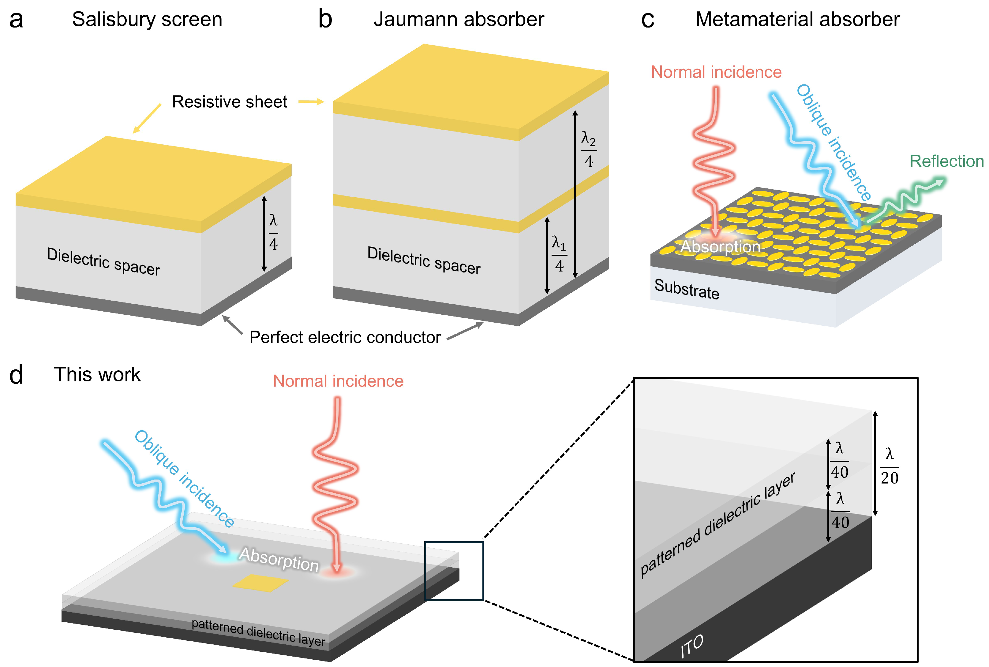
1. Introduction
2. Materials and Methods
3. Results and Discussion
3.1. Two-Dimensional Absorber Optimization
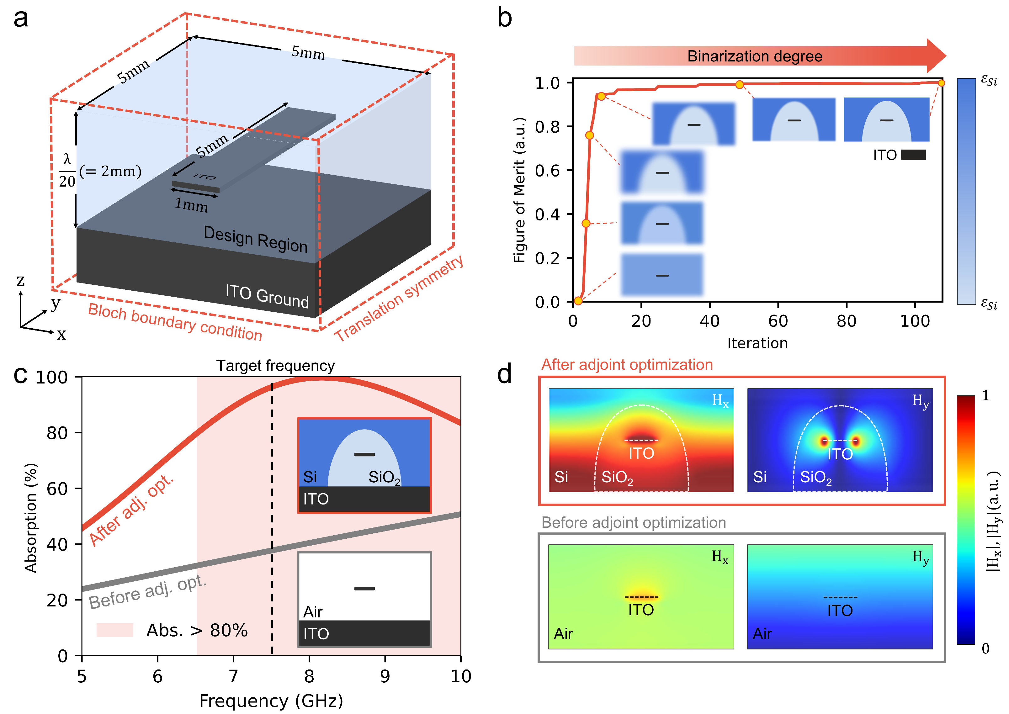
3.1.1. Optimization Under Normal Incidence
3.1.2. Performance Evaluation Under Oblique Incidence
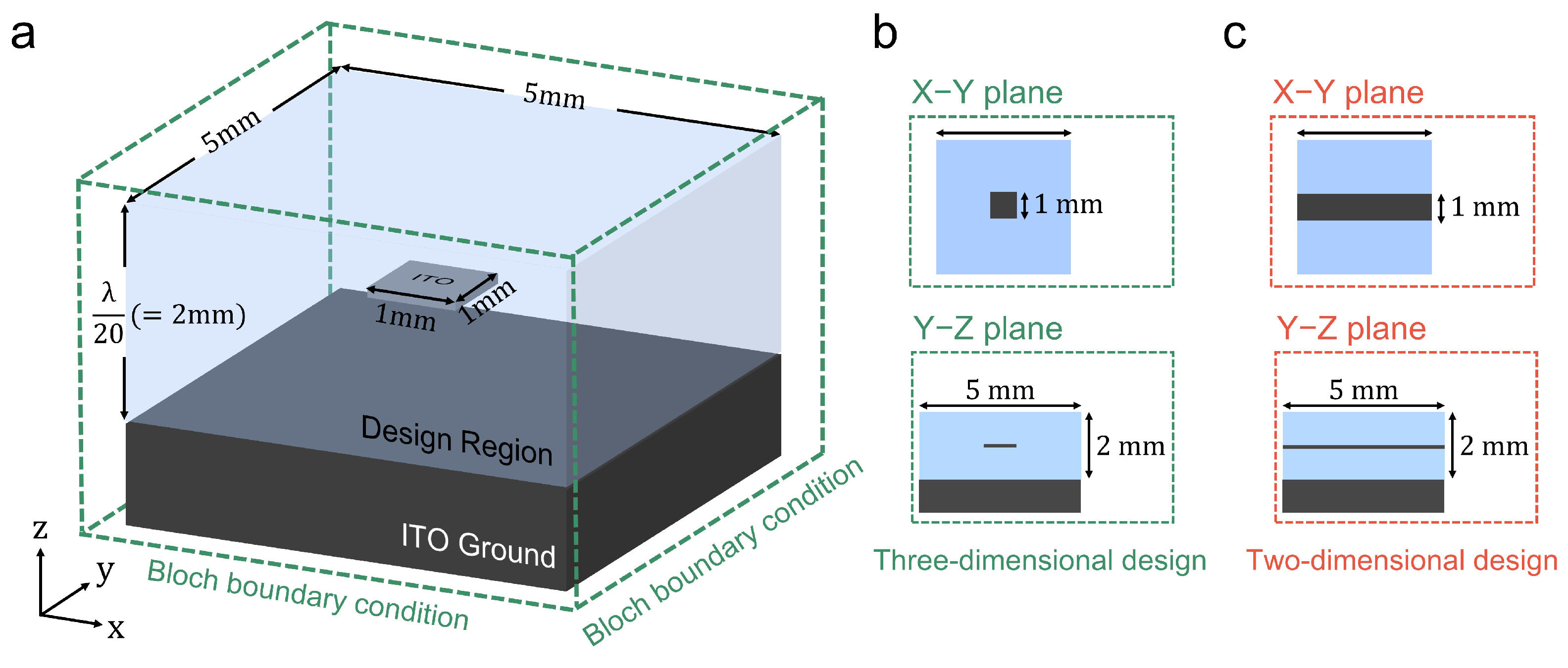
3.2. Three-Dimensional Absorber Optimization
3.2.1. Optimization with Particle Swarm Optimization (PSO)
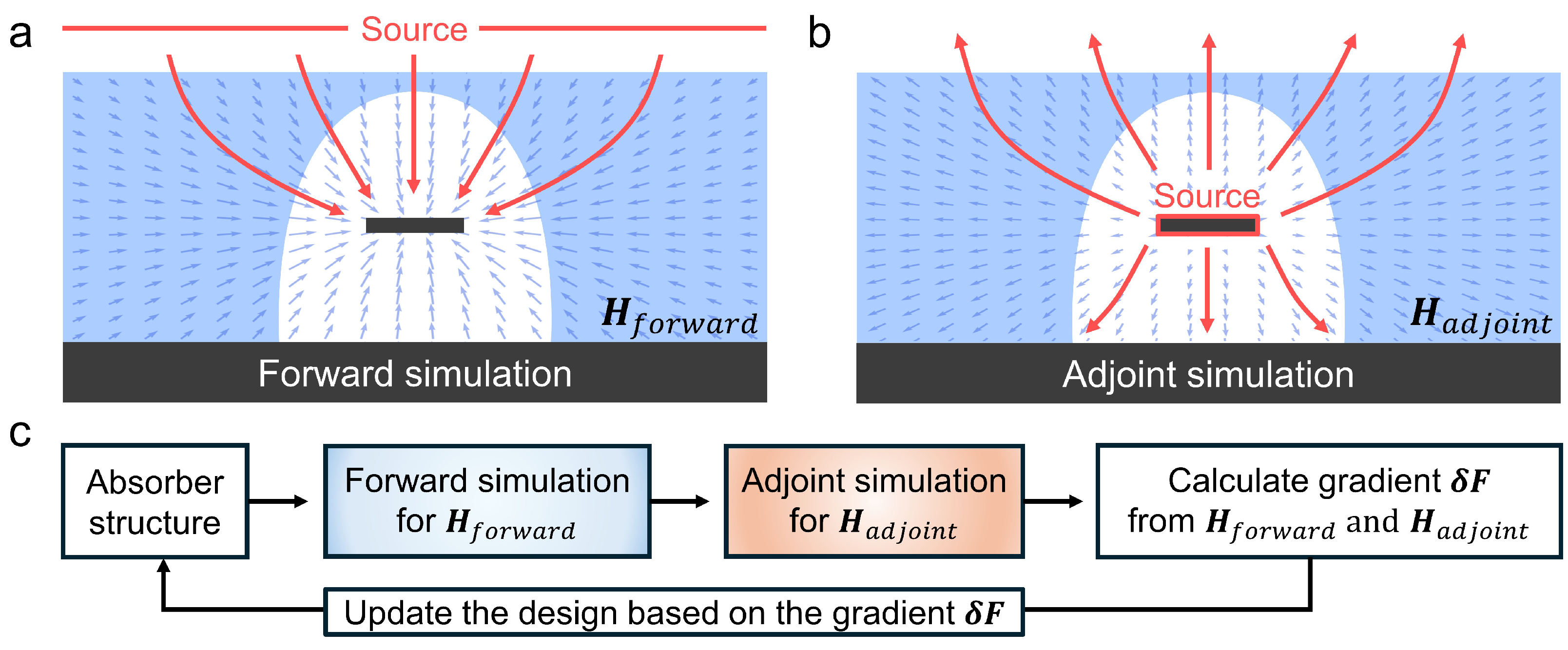
3.2.2. Optimization with the Adjoint Method
3.2.3. Performance Comparison of PSO and Adjoint Optimization
4. Conclusions
Supplementary Materials
Author Contributions
Funding
Data Availability Statement
Conflicts of Interest
Abbreviations
| MMA | Metamaterial Absorber |
| PEC | Perfect Electric Conductor |
| PSO | Particle Swarm Optimization |
| GA | Genetic Algorithm |
| FoM | Figure of Merit |
| FDTD | Finite-Difference Time-Domain |
| ITO | Indium Tin Oxide |
| Si | Silicon |
| SiO2 | Silicon Dioxide |
References
- Smith, D.R.; Pendry, J.B.; Wiltshire, M.C. Metamaterials and negative refractive index. Science 2004, 305, 788–792. [Google Scholar] [CrossRef] [PubMed]
- Chung, H.; Miller, O.D. High-NA achromatic metalenses by inverse design. Opt. Express 2020, 28, 6945–6965. [Google Scholar] [CrossRef] [PubMed]
- Lin, Z.; Liu, V.; Pestourie, R.; Johnson, S.G. Topology optimization of freeform large-area metasurfaces. Opt. Express 2019, 27, 15765–15775. [Google Scholar] [CrossRef] [PubMed]
- Phan, T.; Sell, D.; Wang, E.W.; Doshay, S.; Edee, K.; Yang, J.; Fan, J.A. High-efficiency, large-area, topology-optimized metasurfaces. Light. Sci. Appl. 2019, 8, 48. [Google Scholar] [CrossRef]
- Seo, J.; Jo, J.; Kim, J.; Kang, J.; Kang, C.; Moon, S.W.; Lee, E.; Hong, J.; Rho, J.; Chung, H. Deep-learning-driven end-to-end metalens imaging. Adv. Photonics 2024, 6, 066002. [Google Scholar] [CrossRef]
- Kang, C.; Seo, J.; Jang, I.; Chung, H. Adjoint method-based Fourier neural operator surrogate solver for wavefront shaping in tunable metasurfaces. iScience 2025, 28, 111545. [Google Scholar] [CrossRef]
- Wan, X.; Huang, Z.A.; Wang, J.W.; Wang, W.H.; Li, B.Y.; Xiao, Q.; Wang, X.J.; Wan, J.C.; Cui, T.J. Information metasurface for electromagnetic sensing and wireless communications. Adv. Mater. Technol. 2024, 9, 2301629. [Google Scholar] [CrossRef]
- Wang, Y.; Zhao, C.; Wang, J.; Luo, X.; Xie, L.; Zhan, S.; Kim, J.; Wang, X.; Liu, X.; Ying, Y. Wearable plasmonic-metasurface sensor for noninvasive and universal molecular fingerprint detection on biointerfaces. Sci. Adv. 2021, 7, eabe4553. [Google Scholar] [CrossRef]
- Lee, H.S.; Kuang, Y.P.; Lu, C.Y.; Yen, T.J.; Huang, T.Y. Broadband surface enhanced infrared absorption with multiple Fano resonance by metallic oblique-wire-bundle metamaterial absorbers. Sci. Rep. 2024, 14, 27328. [Google Scholar] [CrossRef]
- Akselrod, G.M.; Huang, J.; Hoang, T.B.; Bowen, P.T.; Su, L.; Smith, D.R.; Mikkelsen, M.H. Large-area metasurface perfect absorbers from visible to near-infrared. Adv. Mater. 2015, 27, 8028–8034. [Google Scholar] [CrossRef]
- Ran, Y.; Shi, L.; Wu, S.; Li, J.; Jin, X.; Hou, Z.; Fan, B.; Wang, J. Optically transparent ultrawideband electromagnetic stealth metasurface for microwave absorption and scattering. IEEE Antennas Wirel. Propag. Lett. 2022, 21, 2412–2416. [Google Scholar] [CrossRef]
- Vaskin, A.; Kolkowski, R.; Koenderink, A.F.; Staude, I. Light-emitting metasurfaces. Nanophotonics 2019, 8, 1151–1198. [Google Scholar] [CrossRef]
- Bae, E.J.; Kang, S.W.; Choi, G.S.; Jang, E.B.; Baek, D.H.; Ju, B.K.; Park, Y.W. Enhanced light extraction from organic light-emitting diodes with micro-nano hybrid structure. Nanomaterials 2022, 12, 1266. [Google Scholar] [CrossRef]
- Choi, G.S.; Kang, S.W.; Bae, E.J.; Jang, E.B.; Baek, D.H.; Ju, B.K.; Park, Y.W. A simple method for fabricating an external light extraction composite layer with rns to improve the optical properties of oleds. Nanomaterials 2022, 12, 1430. [Google Scholar] [CrossRef]
- Gieseler, N.; Moench, S.; Beutel, D.; Pfeifer, W.G.; Domínguez, C.M.; Niemeyer, C.M.; Rockstuhl, C. Chiral plasmonic metasurface assembled by DNA origami. Opt. Express 2024, 32, 16040–16051. [Google Scholar] [CrossRef]
- Xia, F.; Kim, K.; Eliezer, Y.; Han, S.; Shaughnessy, L.; Gigan, S.; Cao, H. Nonlinear optical encoding enabled by recurrent linear scattering. Nat. Photonics 2024, 18, 1067–1075. [Google Scholar] [CrossRef]
- Latifpour, M.H.; Park, B.J.; Yamamoto, Y.; Suh, M.G. Hyperspectral in-memory computing with optical frequency combs and programmable optical memories. Optica 2024, 11, 932–939. [Google Scholar] [CrossRef]
- Carter, M.J.; Resneck, L.; Ra’di, Y.; Yu, N. Flat-Knit, Flexible, Textile Metasurfaces. Adv. Mater. 2024, 36, 2312087. [Google Scholar] [CrossRef]
- Li, Y.; Huang, X.; Liu, S.; Liang, H.; Ling, Y.; Su, Y. Metasurfaces for near-eye display applications. Opto-Electron. Sci. 2023, 2, 230025. [Google Scholar] [CrossRef]
- Shao, R.W.; Wu, J.W.; Li, J.; Meng, S.; Xu, Y.; Wang, Z.X.; Tang, W.; Cheng, Q.; Jin, S.; Cui, T.J. Dual-channel near-field holographic MIMO communications based on programmable digital coding metasurface and electromagnetic theory. Nat. Commun. 2025, 16, 915. [Google Scholar] [CrossRef]
- Landy, N.I.; Sajuyigbe, S.; Mock, J.J.; Smith, D.R.; Padilla, W.J. Perfect metamaterial absorber. Phys. Rev. Lett. 2008, 100, 207402. [Google Scholar] [CrossRef] [PubMed]
- Watts, C.M.; Liu, X.; Padilla, W.J. Metamaterial electromagnetic wave absorbers. Adv. Mater. 2012, 24, OP98–OP120. [Google Scholar] [CrossRef] [PubMed]
- Fante, R.L.; McCormack, M.T. Reflection properties of the Salisbury screen. IEEE Trans. Antennas Propag. 1988, 36, 1443–1454. [Google Scholar] [CrossRef]
- Kim, J.; Han, K.; Hahn, J.W. Selective dual-band metamaterial perfect absorber for infrared stealth technology. Sci. Rep. 2017, 7, 6740. [Google Scholar] [CrossRef]
- Dewangan, L.; Patinavalasa, M.S.; Acharjee, J.; Solunke, Y.; Ghosh, S.; Mishra, N.K. Broadband metamaterial absorber for stealth applications at K-band. AEU-Int. J. Electron. Commun. 2023, 170, 154828. [Google Scholar] [CrossRef]
- Salisbury, W.W. Absorbent Body for Electromagnetic Waves. US Patent 2599944A, 10 June 1952. [Google Scholar]
- Du Toit, L.J. The design of Jauman absorbers. IEEE Antennas Propag. Mag. 1994, 36, 17–25. [Google Scholar] [CrossRef]
- Rozanov, K.N. Ultimate thickness to bandwidth ratio of radar absorbers. IEEE Trans. Antennas Propag. 2000, 48, 1230–1234. [Google Scholar] [CrossRef]
- Kang, J.; Qu, Z.; Duan, J.; Jing, H.; Hao, J.; Song, C.; Wang, J.; Zhang, B. Multispectral flexible ultrawideband metamaterial absorbers for radar stealth and visible light transparency. Opt. Mater. 2023, 135, 113351. [Google Scholar] [CrossRef]
- Lyu, Z.; Zhang, B.; Duan, J.; Yang, Y.; Liu, R.; Wei, Y.; Liu, J. Transparent ultra-broadband absorber based on a tree seedling composite structure. J. Phys. D Appl. Phys. 2021, 55, 095104. [Google Scholar] [CrossRef]
- Deng, G.; Lv, K.; Sun, H.; Yang, J.; Yin, Z.; Chi, B.; Li, X. An ultra-broadband and optically transparent metamaterial absorber based on multilayer indium-tin-oxide structure. J. Phys. Appl. Phys. 2021, 54, 165301. [Google Scholar] [CrossRef]
- Song, Z.; Zhang, R.; Min, P.; Wang, T.; Cao, W.; He, Y.; Wu, L.; Zhu, J.; Qiu, C.W. Inverse design of diffusion–absorption hybrid metasurfaces. Laser Photonics Rev. 2023, 17, 2300280. [Google Scholar] [CrossRef]
- Kim, C.; Bae, M.; Choi, M.; Lee, S.; Lee, M.; Kim, C.; Jung, H.; Chung, H.; Kwon, H. Freeform thin-film lithium niobate mode converter for photon-pair generation. Nanophotonics 2025, 14, 1949–1960. [Google Scholar] [CrossRef] [PubMed]
- Mansouree, M.; McClung, A.; Samudrala, S.; Arbabi, A. Large-scale parametrized metasurface design using adjoint optimization. ACS Photonics 2021, 8, 455–463. [Google Scholar] [CrossRef]
- Kang, C.; Park, C.; Lee, M.; Kang, J.; Jang, M.S.; Chung, H. Large-scale photonic inverse design: Computational challenges and breakthroughs. Nanophotonics 2024, 13, 3765–3792. [Google Scholar] [CrossRef]
- Kennedy, J.; Eberhart, R. Particle swarm optimization. In Proceedings of the ICNN’95-international Conference on Neural Networks, Perth, WA, Australia, 27 November–1 December 1995; Volume 4, pp. 1942–1948. [Google Scholar]
- Rini, D.P.; Shamsuddin, S.M.; Yuhaniz, S.S. Particle swarm optimization: Technique, system and challenges. Int. J. Comput. Appl. 2011, 14, 19–26. [Google Scholar] [CrossRef]
- Gold, H.; Pajovic, S.; Mukherjee, A.; Boriskina, S.V. GAGA for nonreciprocal emitters: Genetic algorithm gradient ascent optimization of compact magnetophotonic crystals. Nanophotonics 2024, 13, 773–792. [Google Scholar] [CrossRef]
- Chung, H.; Miller, O.D. Tunable metasurface inverse design for 80% switching efficiencies and 144 angular deflection. ACS Photonics 2020, 7, 2236–2243. [Google Scholar] [CrossRef]
- Wu, X.; Fu, C.; Li, X.; Meng, Y.; Gao, Y.; Tian, J.; Wang, L.; Huang, Y.; Yang, Z.; Wen, W. Low-frequency tunable acoustic absorber based on split tube resonators. Appl. Phys. Lett. 2016, 109, 043501. [Google Scholar] [CrossRef]
- Mahmud, S.; Islam, S.S.; Almutairi, A.F.; Islam, M.T. A wide incident angle, ultrathin, polarization-insensitive metamaterial absorber for optical wavelength applications. IEEE Access 2020, 8, 129525–129541. [Google Scholar] [CrossRef]
- Holland, J.H. Genetic algorithms. Sci. Am. 1992, 267, 66–73. [Google Scholar] [CrossRef]
- Miller, O. Photonic Design: From Fundamental Solar Cell Physics to Computational Inverse Design. Ph.D. Thesis, EECS Department, University of California, Berkeley, CA, USA, 2012. [Google Scholar]
- Ji, S.; HuYan, S.; Du, L.; Xu, X.; Zhao, J. Efficient Adjoint-Based Shape Optimization Method for the Inverse Design of Microwave Components. IEEE Trans. Microw. Theory Tech. 2024, 73, 494–504. [Google Scholar] [CrossRef]
- Aage, N.; Andreassen, E.; Lazarov, B.S.; Sigmund, O. Giga-voxel computational morphogenesis for structural design. Nature 2017, 550, 84–86. [Google Scholar] [CrossRef] [PubMed]
- Miller, O.D.; Polimeridis, A.G.; Homer Reid, M.; Hsu, C.W.; DeLacy, B.G.; Joannopoulos, J.D.; Soljačić, M.; Johnson, S.G. Fundamental limits to optical response in absorptive systems. Opt. Express 2016, 24, 3329–3364. [Google Scholar] [CrossRef]
- Jackson, J.D. Classical Electrodynamics; John Wiley & Sons: Hoboken, NJ, USA, 1998. [Google Scholar]
- Sihvola, A.H. Electromagnetic Mixing Formulas and Applications; Number 47; IET: London, UK, 1999. [Google Scholar]
- Kang, C.; Seo, D.; Boriskina, S.V.; Chung, H. Adjoint method in machine learning: A pathway to efficient inverse design of photonic devices. Mater. Des. 2024, 239, 112737. [Google Scholar] [CrossRef]
- Bae, M.; Jo, J.; Lee, M.; Kang, J.; Boriskina, S.V.; Chung, H. Inverse design and optical vortex manipulation for thin-film absorption enhancement. Nanophotonics 2023, 12, 4239–4254. [Google Scholar] [CrossRef]
- Yu, S.; Zeng, T.; Pan, X.; Wu, R.; Fan, M.; Xu, G.; Cheng, S. Fabrication of Si3N4–SiC/SiO2 composites using 3D printing and infiltration processing. Ceram. Int. 2021, 47, 28218–28225. [Google Scholar] [CrossRef]
- Ding, G.; He, R.; Zhang, K.; Xie, C.; Wang, M.; Yang, Y.; Fang, D. Stereolithography-based additive manufacturing of gray-colored SiC ceramic green body. J. Am. Ceram. Soc. 2019, 102, 7198–7209. [Google Scholar] [CrossRef]
- Wang, T.; Lu, X.; Wang, A. A review: 3D printing of microwave absorption ceramics. Int. J. Appl. Ceram. Technol. 2020, 17, 2477–2491. [Google Scholar] [CrossRef]
- Oskooi, A.F.; Roundy, D.; Ibanescu, M.; Bermel, P.; Joannopoulos, J.D.; Johnson, S.G. MEEP: A flexible free-software package for electromagnetic simulations by the FDTD method. Comput. Phys. Commun. 2010, 181, 687–702. [Google Scholar] [CrossRef]
- Parsianpour, E.; Akhavan, O.; Amini, M. Characterization and structural property of indium tin oxide thin films. Adv. Mater. Phys. Chem. 2017, 7, 123–130. [Google Scholar] [CrossRef]
- McGuire, G.E. Semiconductor Materials and Process Technology Handbook; Electronics Reliability and Measurement Technology; William Andrew: New York, NY, USA, 1988. [Google Scholar]
- Gray, P.R.; Hurst, P.J.; Lewis, S.H.; Meyer, R.G. Analysis and Design of Analog Integrated Circuits, 6th ed.; John Wiley & Sons: Hoboken, NJ, USA, 2024. [Google Scholar]
- Svanberg, K. A Class of Globally Convergent Optimization Methods Based on Conservative Convex Separable Approximations. SIAM J. Optim. 2002, 12, 555–573. [Google Scholar] [CrossRef]
- Johnson, S.G. The NLopt Nonlinear-Optimization Package. Available online: https://github.com/stevengj/nlopt (accessed on 5 June 2025).
- Zeng, X.; Cheng, X.; Yu, R.; Stucky, G.D. Electromagnetic microwave absorption theory and recent achievements in microwave absorbers. Carbon 2020, 168, 606–623. [Google Scholar] [CrossRef]
- Alwan, E.A.; Kiourti, A.; Volakis, J.L. Indium tin oxide film characterization at 0.1–20 GHz using coaxial probe method. IEEE Access 2015, 3, 648–652. [Google Scholar] [CrossRef]
- Castro Neto, A.H.; Guinea, F.; Peres, N.M.; Novoselov, K.S.; Geim, A.K. The electronic properties of graphene. Rev. Mod. Phys. 2009, 81, 109–162. [Google Scholar] [CrossRef]
- Eriksson, G. Efficient 3D simulation of thin conducting layers of arbitrary thickness. In Proceedings of the 2007 IEEE International Symposium on Electromagnetic Compatibility, Qingdao, China, 23–26 October 2007; pp. 1–6. [Google Scholar]
- Bendsoe, M.P.; Sigmund, O. Topology Optimization: Theory, Methods, and Applications; Springer Science & Business Media: Cham, Switzerland, 2013. [Google Scholar]
- Pan, C.C.; Bae, M.; Wang, H.; Lim, J.; Unnithan, R.R.; Yang, J.; Chung, H.; Kim, S. Inverse Design of Chiral Structures for Giant Helical Dichroism. arXiv 2025, arXiv:2501.12825. [Google Scholar] [CrossRef]
- Chauhan, N.; Kartikeyan, M.V.; Mittal, A. A modified particle swarm optimizer and its application to the design of microwave filters. J. Infrared Millim. Terahertz Waves 2009, 30, 598–610. [Google Scholar] [CrossRef]
- Ulker, E.D.; Ulker, S. Application of particle swarm optimization to microwave tapered microstrip lines. arXiv 2014, arXiv:1403.2842. [Google Scholar] [CrossRef]
- Islam, M.T.; Misran, N.; Take, T.C.; Moniruzzaman, M. Optimization of microstrip patch antenna using particle swarm optimization with curve fitting. In Proceedings of the 2009 International Conference on Electrical Engineering and Informatics, Bangi, Malaysia, 5–7 August 2009; Volume 2, pp. 711–714. [Google Scholar]
- Mirjalili, S.; Wang, G.G.; Coelho, L.d.S. Binary optimization using hybrid particle swarm optimization and gravitational search algorithm. Neural Comput. Appl. 2014, 25, 1423–1435. [Google Scholar] [CrossRef]
- Molesky, S.; Lin, Z.; Piggott, A.Y.; Jin, W.; Vucković, J.; Rodriguez, A.W. Inverse design in nanophotonics. Nat. Photonics 2018, 12, 659–670. [Google Scholar] [CrossRef]
- Piggott, A.Y.; Lu, J.; Lagoudakis, K.G.; Petykiewicz, J.; Babinec, T.M.; Vučković, J. Inverse design and demonstration of a compact and broadband on-chip wavelength demultiplexer. Nat. Photonics 2015, 9, 374–377. [Google Scholar] [CrossRef]
- Iwaszczuk, K.; Strikwerda, A.C.; Fan, K.; Zhang, X.; Averitt, R.D.; Jepsen, P.U. Flexible metamaterial absorbers for stealth applications at terahertz frequencies. Opt. Express 2011, 20, 635–643. [Google Scholar] [CrossRef] [PubMed]
- Hossain, M.B.; Faruque, M.R.I.; Islam, M.T.; Singh, M.; Jusoh, M. Triple band microwave metamaterial absorber based on double E-shaped symmetric split ring resonators for EMI shielding and stealth applications. J. Mater. Res. Technol. 2022, 18, 1653–1668. [Google Scholar] [CrossRef]
- Karaaslan, M.; Bağmancı, M.; Ünal, E.; Akgol, O.; Sabah, C. Microwave energy harvesting based on metamaterial absorbers with multi-layered square split rings for wireless communications. Opt. Commun. 2017, 392, 31–38. [Google Scholar] [CrossRef]
- Mohammed, S.A.; Albadri, R.A.K.; Al-Badri, K.S.L. Simulation of the microwave five-band a perfect metamaterial absorber for the 5G communication. Heliyon 2023, 9, e19466. [Google Scholar] [CrossRef]
- Holman, A.; Xu, Y.; Sun, X.; Wu, J.; Wang, M.; Seo, B.; Yu, N.; Will, S. Trapping of Single Atoms in Metasurface Optical Tweezer Arrays. arXiv 2024, arXiv:2411.05321. [Google Scholar]

Disclaimer/Publisher’s Note: The statements, opinions and data contained in all publications are solely those of the individual author(s) and contributor(s) and not of MDPI and/or the editor(s). MDPI and/or the editor(s) disclaim responsibility for any injury to people or property resulting from any ideas, methods, instructions or products referred to in the content. |
© 2025 by the authors. Licensee MDPI, Basel, Switzerland. This article is an open access article distributed under the terms and conditions of the Creative Commons Attribution (CC BY) license (https://creativecommons.org/licenses/by/4.0/).
Share and Cite
Jang, E.; Cho, J.; Kang, C.; Chung, H. Inverse Design of Ultrathin Metamaterial Absorber. Nanomaterials 2025, 15, 1024. https://doi.org/10.3390/nano15131024
Jang E, Cho J, Kang C, Chung H. Inverse Design of Ultrathin Metamaterial Absorber. Nanomaterials. 2025; 15(13):1024. https://doi.org/10.3390/nano15131024
Chicago/Turabian StyleJang, Eunbi, Junghee Cho, Chanik Kang, and Haejun Chung. 2025. "Inverse Design of Ultrathin Metamaterial Absorber" Nanomaterials 15, no. 13: 1024. https://doi.org/10.3390/nano15131024
APA StyleJang, E., Cho, J., Kang, C., & Chung, H. (2025). Inverse Design of Ultrathin Metamaterial Absorber. Nanomaterials, 15(13), 1024. https://doi.org/10.3390/nano15131024