Article

Boosting Photoresponse Performance and Stability of Photoelectrochemical Photodetectors by Chemical Bath Depositing Multilayer MoS2 on ZnO Electrode

Xinjiang Key Laboratory of Luminescence Minerals and Optical Functional Materials, School of Physics and Electronic Engineering, Xinjiang Normal University, Urumqi 830054, China
*
Authors to whom correspondence should be addressed.
Nanomaterials 2025, 15(12), 875; https://doi.org/10.3390/nano15120875
Submission received: 15 May 2025 / Revised: 28 May 2025 / Accepted: 3 June 2025 / Published: 6 June 2025

Abstract

ZnO nanorods are promising nanomaterials for photoelectrochemical photodetectors (PEC PDs). However, the weak photocurrent density, delayed response, and low stability of ZnO are major drawbacks for their applications. To address these challenges, we integrated multilayer MoS2 nanosheets with ZnO nanorods using a chemical bath deposition method. The resulting ZnO/MoS2 heterojunction achieved a photocurrent density of 1.02 mA/cm2 (~20 times higher than that of bare ZnO), ultrafast response times (90/150 ms), and 92% stability retention over 3600 s. These enhancements originated from suppressed charge recombination and accelerated water oxidation kinetics. Our work provides another possible energy-saving route toward developing high-efficiency and stable ZnO-based photoanodes for practical applications in PEC PDs.

Graphical Abstract

1. Introduction

Photoelectrochemical (PEC) photodetectors (PDs) convert light into electrical signals using a photoelectrochemical process. They have made rapid strides in the fields of information devices and energy conversion owing to their low cost, simple production method, low working voltage, and high sensitivity. In recent years, PD devices based on zinc oxide (ZnO) nanostructures have found extensive application because of their direct bandgap semiconductor properties, strong electron mobility, great chemical stability, high exciton binding energy (60 meV), eco-friendly nature, and cost-effectiveness [1,2,3]. In particular, aligned ZnO nanorod arrays can absorb and trap more incident photons, which lowers the channel resistance and improves the device’s conductivity. Moreover, the directional transport of photogenerated carriers through the vertical structure can efficiently enhance the electron–hole pair separation [4]. Nevertheless, the poor photocurrent density, slow response (often > 1000 ms), and low stability of pure ZnO are significant disadvantages for its PD applications [5]. Constructing a heterostructure using ZnO nanorods and suitable semiconductor materials is a practical way to break the above restrictions.
MoS2 is an ideal candidate material for mitigating the aforementioned limitations of ZnO due to its superior optoelectronic properties, including a high internal quantum efficiency (~85%); an exceptional on/off current ratio (~107), surpassing that of graphene-based devices by several orders of magnitude (Ilight/Idark ≈ 4 in the literature) [6]; and good carrier mobility (>200 cm2 V−1 s−1) [7]. In addition, MoS2 and ZnO can easily form a type-II heterojunction, which is conducive to improving the photocurrent density and speeding up the response time by increasing the spacing of photogenerated carriers. For example, Lamouchi et al. constructed a ZnO/MoS2 heterostructure to observe the benefits of a type-II heterojunction: its photocurrent density value was ~7 times higher than that of pure ZnO [8]. Gautam et al. created ZnO/MoS2 PDs, which had a faster response time (tres = 2.46 s) than pure ZnO PDs (tres = 3.75 s) [9]. Ma et al. studied ZnO/MoS2 PDs, which also exhibited fast response/recovery times (tres/trec = 0.15 s/0.17 s) [10]. In addition, the stability of ZnO-based electrodes, primarily limited by the oxidation kinetics of photogenerated holes at the electrode/electrolyte interface, can be enhanced through a rational heterostructure design that leverages the abundant active sites at MoS2 edges to accelerate photoelectrochemical reaction kinetics [11]. Different deposition methods, such as chemical vapor deposition, solgel-assisted synthesis, dual-phase solid-state dewetting, and drop casting, can be used to deposit MoS2 on a ZnO surface for photodetector applications [9,10,12,13]. Nevertheless, there are still desirable, cheaper, and efficient high-performance techniques with a lower thermal budget (i.e., the total thermal energy input required during fabrication [14]) and without a special gas environment or high-power demand for creating controlled heterostructures based on MoS2.
Chemical bath deposition (CBD) is a versatile technique frequently used in solar cells [15], sodium-ion batteries [16], gas sensors [17], and supercapacitors [18] due to its low processing temperature (typically below 100 °C), reproducibility, easy-to-change parameters, and low cost. Additionally, this technique enables the optimization of films’ thickness, grain size, crystalline quality, and shape by regulating a growth parameter, such as deposition time, molarity, solution temperature, and so on. Considering these advantages, employing CBD to deposit MoS2 on ZnO could be a successful strategy with which to obtain superior quality ZnO/MoS2 PEC PDs.
To improve the main factors restricting the application of ZnO PEC PDs, such as weak photocurrent density, delayed response, and low stability, an energy-efficient CBD method was used in this study to prepare ZnO/MoS2 heterojunctional PEC PDs. The microstructure of the ZnO/MoS2 photoanode and the layer number information of MoS2 in the heterojunction were analyzed via transmission electron microscopy (TEM) and Raman spectroscopy, and photoelectrochemical activity, PEC PD performance, and stability were investigated in detail. EIS spectra, Bode phase plots, and open-circuit photovoltage vs. time curve measurements suggest that the incorporation of MoS2 could improve the interface electron transfer, resulting in an enhanced PEC PD property. Based on the results, a possible mechanism is proposed to explain the enhanced performance of ZnO/MoS2 photoanodes. The results offer a new insight into the development of efficient and stable heterogeneous PEC PDs.

2. Materials and Methods

2.1. Preparation of the ZnO Photoanode

Before the hydrothermal reaction, 5 mL of zinc acetate solution (5 mM, Macklin, Shanghai, China) was dropped onto an ITO conductive substrate. After drying, it was calcined at 350 °C for 2 h. Subsequently, the pre-treated conductive substrate was immersed in a reaction solution consisting of hexamethylenetetramine (25 mM, SCR, Shanghai, China) and zinc nitrate hexahydrate (25 mM, SCR, Shanghai, China) dissolved in 14 mL of water, followed by the hydrothermal reaction at 90 °C for 3 h. The hydrothermal growth process was repeated three times to obtain ~1.58 μm long and ~137 nm wide ZnO nanorods on ITO. Then, the ZnO photoanode was ultrasonicated in anhydrous ethanol for 5 min, followed by rinsing in deionized water for another 5 min under ultrasonication. This ethanol–water cleaning cycle was repeated three times to ensure the thorough removal of loosely adhered particles. Finally, the sample was dried at 60 °C for 6 h in a vacuum drying oven.

2.2. Fabrication of the ZnO/MoS2 Photoanode

The ZnO/MoS2 photoanode was prepared using the CBD method. Firstly, (NH4)2MoS4 (26 mg, 99.95% purity, Alfa, NJ, USA) was dissolved in 50 mL of deionized water to achieve a 3.93 mM solution. Then, 100 μ L of hydrazine hydrate (80% AR, Kermel, Tianjin City, China) was added to the above solution. After that, the ZnO photoanode (~1.58 μm length, ~137 nm width nanorods on the ITO surface) was positioned in the solution at a 45° angle to the beaker wall (ZnO-coated side pointing downward), and deposition proceeded at 90 °C and 200 rpm stirring for 40 min to fabricate the ZnO/MoS2 photoanode, with an extended reaction time to 80 min yielding the ZnO/MoS2-80 heterojunction for comparison. The preparation procedure of the ZnO/MoS2 photoanode is illustrated in Figure 1.

2.3. Characterization

TEM (FEI Tecnai G2 F20, FEI, Hillsboro, OR, USA) was used to evaluate the samples’ morphologies and microstructures. Prior to TEM testing, we scraped the nanorods off the ITO substrate using a diamond blade. The collected material was then subjected to ultrasonic dispersion in anhydrous isopropyl alcohol at 40 kHz for 10 min to isolate individual nanorods for TEM characterization. The Raman spectra of the as-fabricated materials were obtained using a Horiba Jobin Yvon LabRam apparatus (Paris, France.) via excitation with a 532 nm laser.

2.4. Photoelectrochemical Measurements

A three-electrode (as-prepared electrode, Pt wire, and Ag/AgCl electrode) electrochemical workstation (Chenhua, Shanghai, China.) configuration was implemented to test the photoelectrochemical properties of the produced photoanodes. The light source was a xenon lamp (100 mW/cm2). The electrolyte was an aqueous solution comprising a combination of 0.1 M Na2S·9H2O and 0.02 M Na2SO3. Cyclic linear sweep voltammetry was used to measure the I–V curves from −1 to 1 V vs. Ag/AgCl at a scan rate of 30 mV/s. The transient photocurrent response was measured at the potential of 0.1 V vs. Ag/AgCl with a switching duration of 5 s. Under open-circuit voltage conditions, the EIS spectra were recorded in the frequency range of 0.01 Hz to 100 kHz. A diagram of the ZnO/MoS2 PEC PDs performance test is illustrated in Figure S1 in Supporting Information.

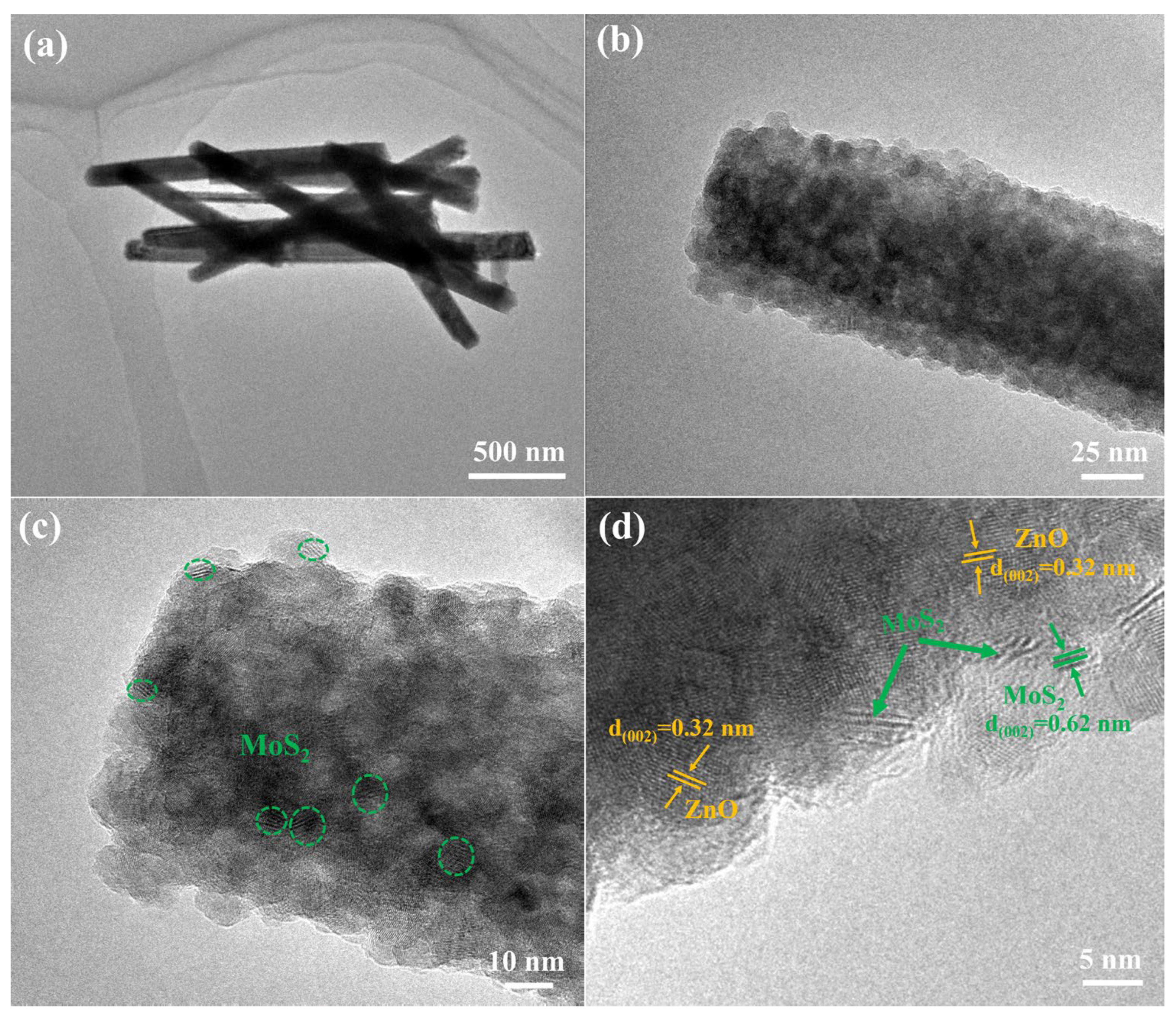
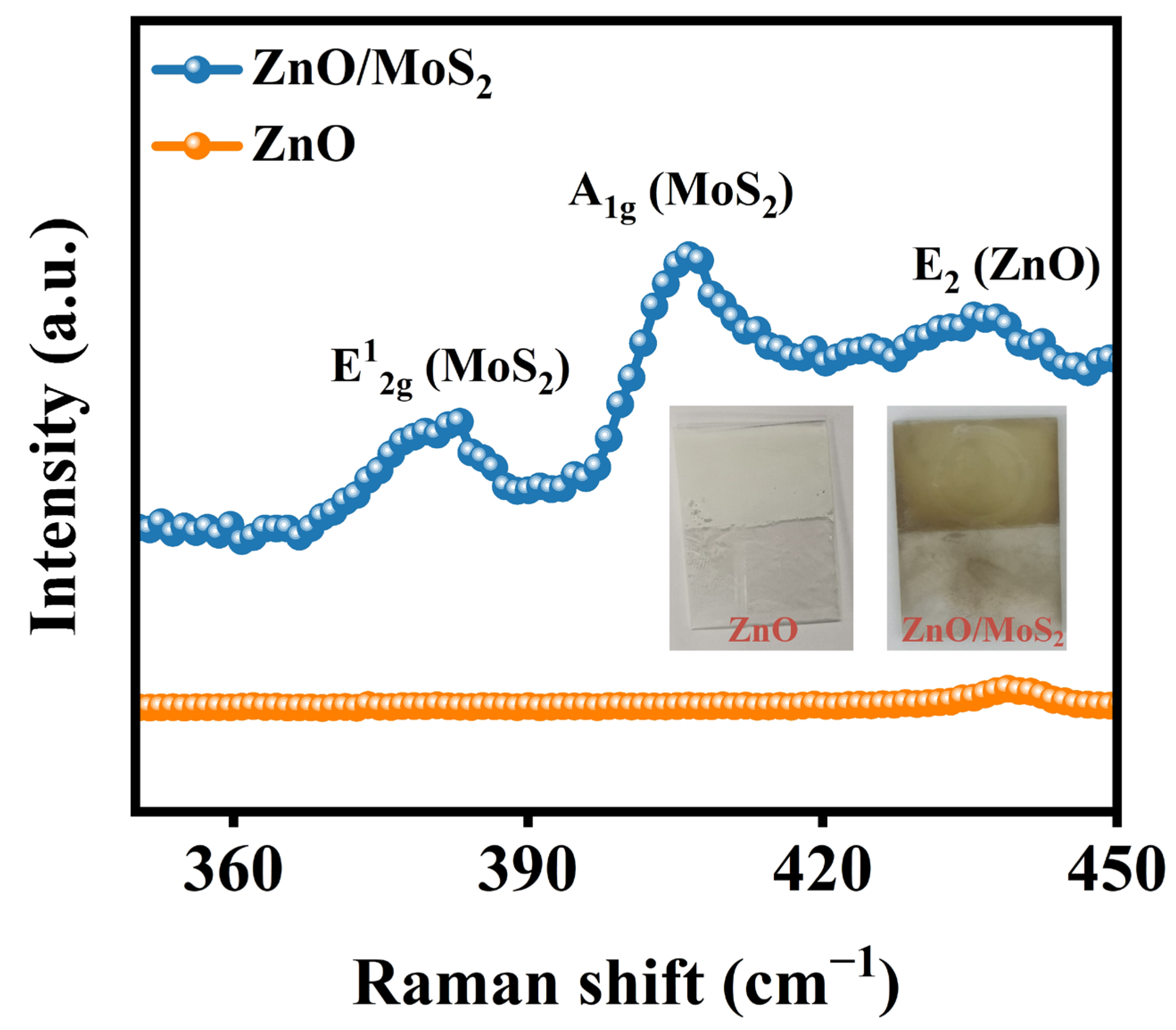
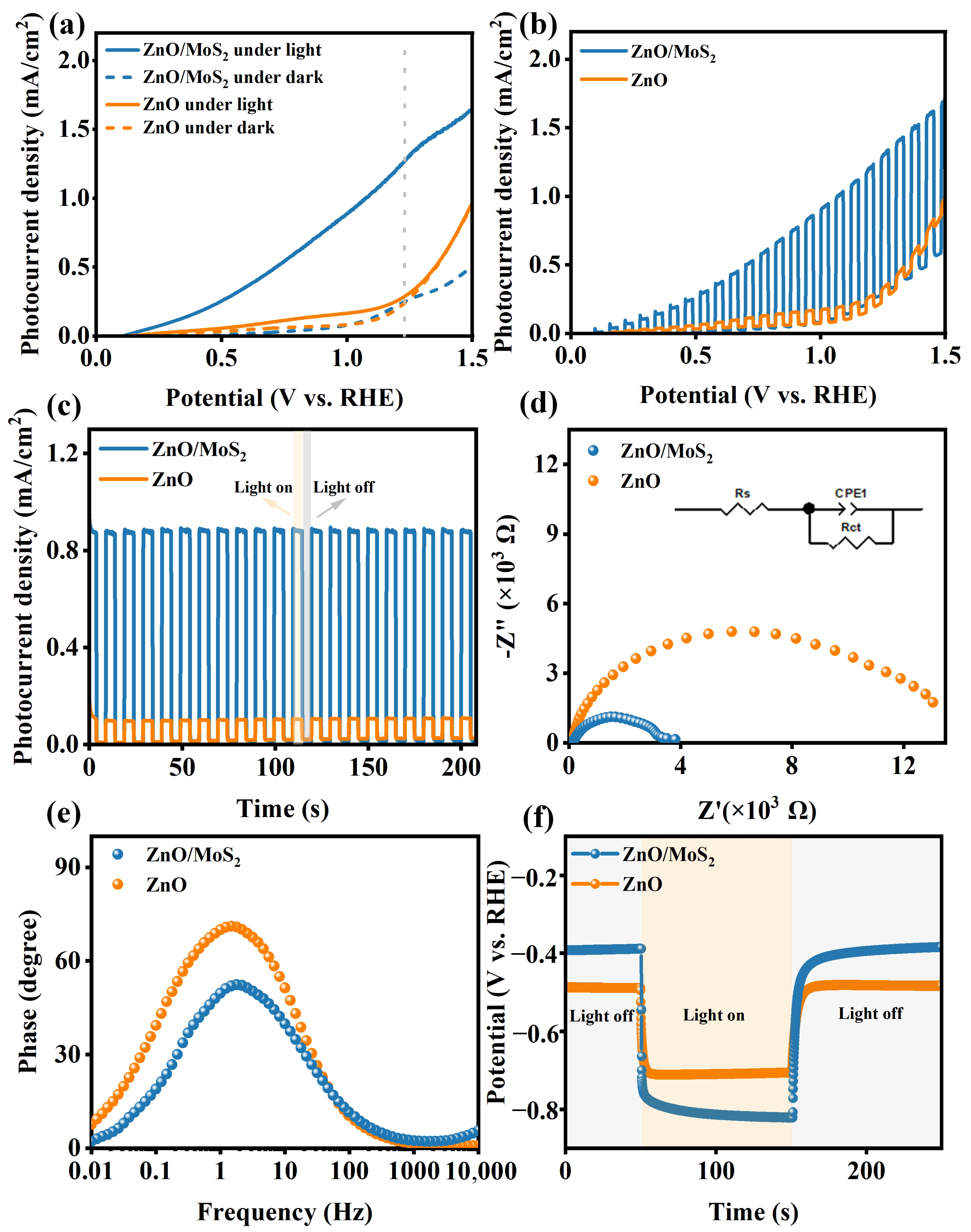
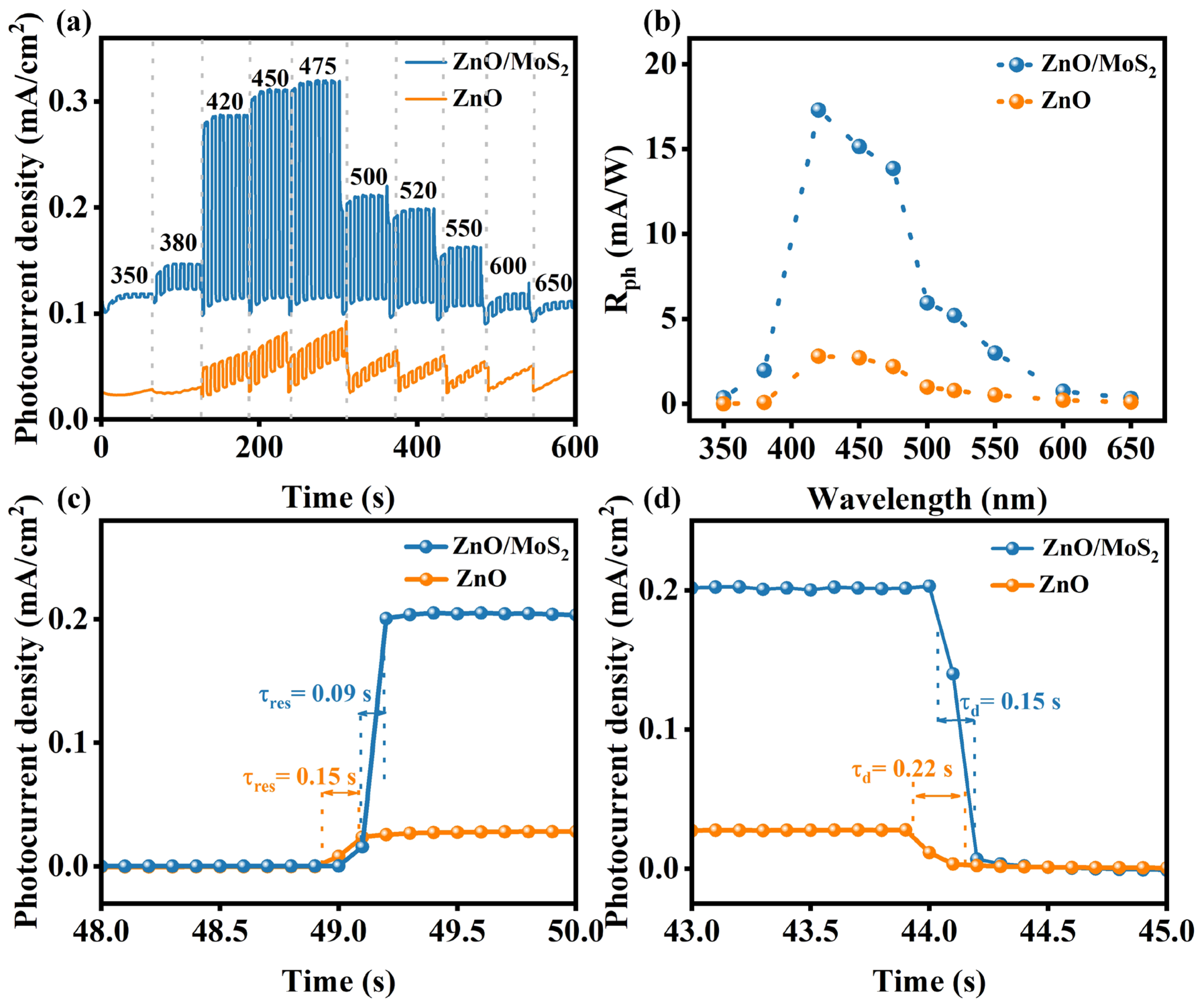
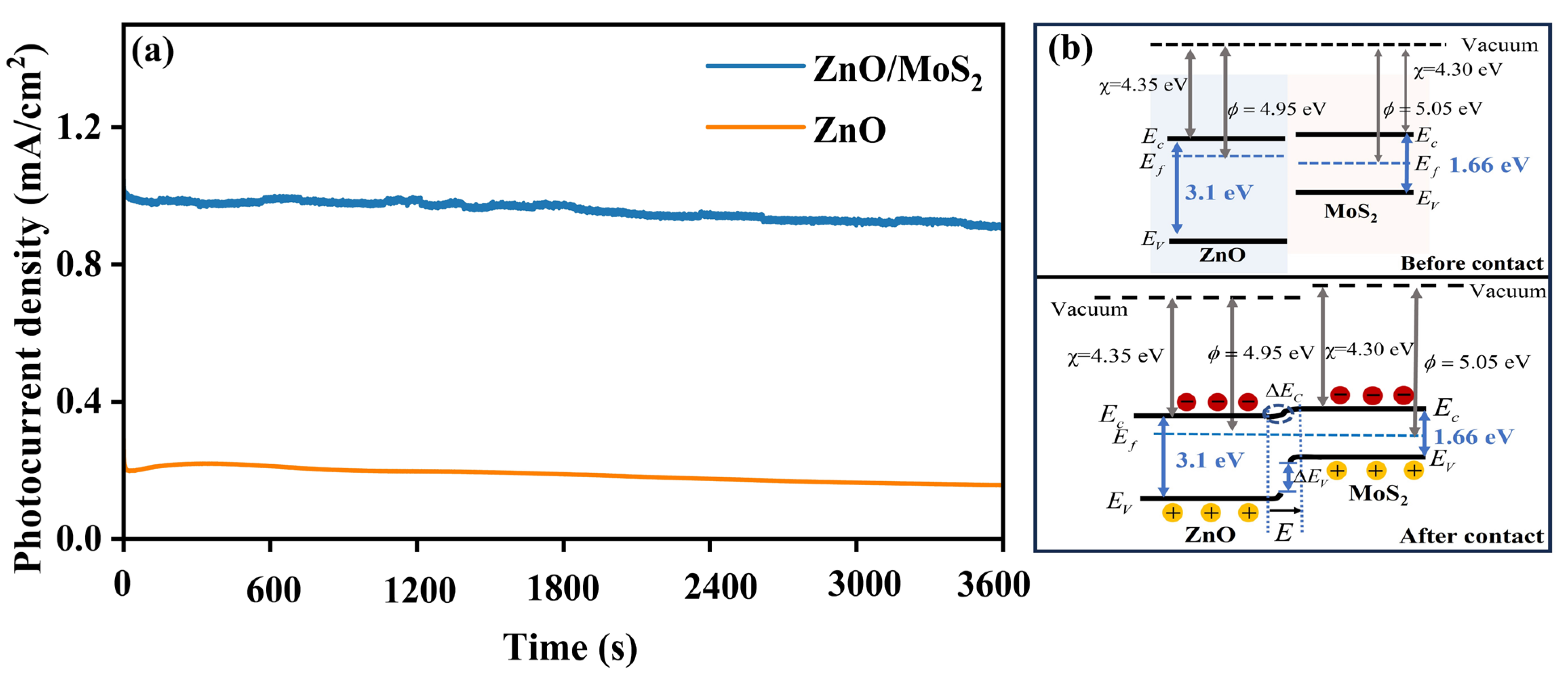
3. Results and Discussion

The morphologies and microstructure of the produced ZnO/MoS2 heterostructure were investigated via transmission electron microscopy (TEM) and high-resolution TEM (HRTEM). As seen in Figure 2a, the ZnO/MoS2 heterojunction had a uniform nanorod-like appearance, with the average length and width being approximately 1.58 μm and 137 nm, respectively. The TEM images, after magnification (Figure 2b), show that the ZnO nanorods were composed of small particles, while MoS2 was not observed. The further enlarged TEM images (Figure 2c) show that the ZnO surfaces were adorned with several MoS2 nanosheets, and the lattice spacing could be determined based on the clear view provided by the HRTEM images (Figure 2d). A lattice spacing of 0.62 nm was indexed to the (002) plane of 2H-MoS2 [19]. Additionally, a 0.32 nm lattice spacing appeared in good agreement with the (0110) plane of ZnO [20]. The TEM characterization revealed the successful formation of a ZnO/MoS2 heterostructure, which would facilitate the transfer of photogenerated carriers.
Raman spectra were further obtained to investigate the chemical structure of the ZnO/MoS2 photoanode. As illustrated in Figure 3, the pure ZnO photoanode exhibited a peak situated at roughly 438 cm−1, which was indexed to the E2 mode of ZnO [21]. Conversely, the ZnO/MoS2 photoanode exhibited two obvious peaks at 381 cm−1 and 406 cm−1, in addition to the ZnO characteristic peaks, corresponding to the in-plane lattice vibration ( E 2 g 1 ) and out-of-plane lattice vibration ( A 1 g ) of MoS2 [22]. The peak value difference between E 2 g 1 and A 1 g was 25 cm−1, indicating that MoS2 in the ZnO/MoS2 photoanode was four-layered (multilayer; ≥3 layers) [23,24]. This value aligns with the reported values for a pure MoS2 photodetector, while multilayer MoS2 demonstrated enhanced light absorption capacity compared to few-layer structures in optoelectronic applications [25]. Moreover, a leftward shift in the ZnO peak position was observed in the heterojunction compared to pristine ZnO, which was attributed to strong interfacial electronic interactions between the two semiconductors [26,27]. Figure S2 displays the ZnO/MoS2-80 Raman spectrum. We can see that the photoanode has two distinct distinctive peaks that belong to MoS2 at 380 cm−1 and 406 cm−1, with a peak separation of 26 cm−1, exceeding the 25 cm−1 value in ZnO/MoS2-40, indicating that the thickness of MoS2 increased with the increase in reaction time [28]. However, the peak of E2-ZnO is invisible, potentially due to laser shielding by the MoS2 shell. Prior studies on ZnO-based nanocables have also noted similar occurrences [29]. Figure S3 shows the statistical results for the Raman spectra data for multiple positions of the ZnO/MoS2 photoanodes. The average peak positions of MoS2 in the ZnO/MoS2 heterojunction were 380 ± 0.81 cm−1 ( E 2 g 1 peak of MoS2) and 405.6 ± 0.63 cm−1 ( A 1 g peak of MoS2). The small deviations indicated the uniform deposition of MoS2 on the ZnO surface.
Linear sweep curves were determined for the pure ZnO and ZnO/MoS2 heterojunction photoanodes using a typical three-electrode configuration under continuous and chopped 100 mW/cm2 illumination (Figure 4a,b). The ZnO/MoS2-40 photoanode showed noticeably higher photocurrent densities throughout the entire potential window compared to its ZnO and ZnO/MoS2-80 counterparts, achieving 1.02 mA/cm2 at 1.23 V vs. RHE (the standard reversible potential for water oxidation), which was ~20 times and ~4.6 times greater than that of the pure ZnO (0.05 mA/cm2) and ZnO/MoS2-80 (0.22 mA/cm2, Figure S4a,b) photoanodes, respectively. Additionally, the initial potentials of the ZnO, ZnO/MoS2-40, and ZnO/MoS2-80 photoanodes were approximately 136 mV, 110 mV, and 127 mV, respectively. The ZnO/MoS2-40 photoanode exhibited a significantly lowest initial potential value, indicating that optimal MoS2 modification effectively reduce the water oxidation energy barrier of ZnO, thereby promoting the water oxidation kinetics [28]. The above results determined that ZnO/MoS2-40 was the structure with the highest light response intensity.
The photocurrent responses of the ZnO and ZnO/MoS2 photoanodes at 1 V vs. RHE under multiple switching cycles are also shown in Figure 4c. The ZnO/MoS2 photoanode had a greater photocurrent response intensity than the pure ZnO photoanode, demonstrating that its electronic lifetime and separation efficiency are significantly higher than those of a single ZnO photoanode. Furthermore, with instantaneous light-switching intervals, we could see that every manufactured photoelectrode displayed a consistent increase and decrease in photocurrent density, indicating their high photo-responsiveness and reversibility. Even after 200 s of rapid switching, the ZnO/MoS2 photoanode’s photocurrent density and reproducibility remained constant, demonstrating its great stability and consistency.
Impedance spectra of the ZnO and ZnO/MoS2 photoanodes were obtained to study the dynamics of photogenerated charge transport, as shown in Figure 4d. The corresponding equivalent circuit model is presented in the inset, where Rₛ, CPE, and Rct represent the series resistance between the photoanode and the ITO substrate, the constant phase element, and the charge transfer resistance at the photoanode–electrolyte interface, respectively. The measured Rs values for the ZnO and ZnO/MoS2 photoanodes were 120.0 Ω and 121.9 Ω, respectively. The minimal difference in the Rs values indicates that their impedance spectra were recorded under similar environments, enabling a direct comparison of the Rct values. Specifically, the Rct values were as follows: ZnO/MoS2 (3.14 kΩ) < ZnO (12.32 kΩ). The significantly lower Rct value of the ZnO/MoS2 photoanode suggests that interfacial engineering effectively enhances the charge separation efficiency while accelerating the surface water oxidation kinetics [30]. This result supports the photocurrent response performance observed in Figure 4c.
The Bode diagram of the ZnO and ZnO/MoS2 photoanodes more directly reflects the influence of heterojunction construction on the carrier dynamics (Figure 4e). According to previous reports, the photoanodes displayed greater phase values at low-frequency peaks, suggesting that the charge transfer at the electrode/electrolyte interface significantly restricted the oxidation of the electrode water [31,32]. As shown in Figure 4e, the characteristic peaks of the ZnO/MoS2 and ZnO photoanodes are both at low frequencies (around 1 Hz), and the low-frequency peak of ZnO/MoS2 photoanode is significantly lower than that of the ZnO photoanode, revealing quicker charge transfer kinetics at the electrode/electrolyte interface of the ZnO/MoS2 photoanode.
The open-circuit photovoltage ΔOCP (VlightVdark) curves of the as-fabricated photoanodes were determined to identify the band bending degree and the surface charge transfer mechanism. As illustrated in Figure 4f, the ΔOCP value of the ZnO/MoS2 photoanode was 0.42 V, which is ~52.4% higher than that of pristine ZnO (0.22 V). This suggests that the ZnO/MoS2 photoanode has quicker charge transfer and greater band bending at its photoanode/electrolyte interface.
The sensitivity performance of the ZnO/MoS2 and ZnO PEC-type PDs at different indicative light wavelengths (350, 380, 420, 450, 475, 500, 520, 550, 600, and 650 nm) was investigated. As displayed in Figure 5a, compared with the ZnO PEC PD, the photoresponse of the ZnO/MoS2 PEC PD was more significant for each single-channel light, which can be ascribed to the efficient charge separation via type-II heterojunction formation between ZnO and MoS2. In addition, the Iph values of the ZnO/MoS2 PEC PD increased at a wavelength from 350 to 475 nm, and a maximum Iph value of ~210 μA/cm2 at 475 nm was achieved, which is seven times greater than that of the ZnO PEC PD (~30 μA/cm2) under the same conditions. As the wavelength redshifted from 500 to 650 nm, the Iph of the ZnO/MoS2 PEC PD decreased. Through power law analysis [33], we obtained that the weak capture coefficients of ZnO and ZnO/MoS2 PDs were 1.21 and 1.14, respectively (as shown in Figure S5, Supporting Information. The lower γ for ZnO/MoS2 indicates a reduction in the capture effect due to interface charge transfer. Moreover, the rejection ratio (RR = Iph (@475 nm, ~210 μA/cm2)/Iph (@350 nm, ~3 μA/cm2)) for the fabricated heterojunction device was ~70, which indicates that the photodetector exhibits a relatively high signal-to-noise ratio. The corresponding photoresponsivity (Rph) values (Rph = Iph/P) of the ZnO/MoS2 and ZnO PEC-type PDs at different wavelengths were also calculated (Figure 5b). The ZnO/MoS2 photoanode exhibited a superior photoresponse (Rph) within the 350–600 nm range compared to the ZnO nanorods, which might be driven by dual enhancement mechanisms. Firstly, as shown in Figure S7, the structurally ordered ZnO nanorods can absorb and utilize light in the ultraviolet–visible range, which is due to their highly organized structure inducing significant light-scattering effects [10]. These scattering effects synergize with the intrinsic visible-light absorption capacity of multilayer MoS2, collectively improving the spectral utilization across the specified range. Furthermore, the type-II heterojunction at the ZnO/MoS2 interface facilitates a directional carrier transport while suppressing recombination losses, as validated by charge dynamics analyses in prior heterostructure studies [34,35]. The strategic coupling of these spectral broadening structural features with optimized interfacial charge transfer pathways constitutes the fundamental origin of the enhanced Rph performance. When the wavelength was extended from 350 to 420 nm, the associated Rph increased from 0.36 to 17.29 mA/W before progressively falling to 0.32 mA/W for the ZnO/MoS2 PEC PD. At 420 nm light irradiation, the highest Rph value (17.29 mA/W) of the ZnO/MoS2 PEC PD was recorded and appeared to be almost 6.2 times higher than that of the ZnO PEC PD (2.8 mA/W). The ZnO/MoS2 photoanode showed the highest response in the visible region, which can be attributed to the synergistic effect of light scattering by the ZnO nanorods and intrinsic light absorption in the electrolyte [36,37]. Additionally, it was also much more significant than that reported for pure MoS2 PDs (0.17 mA/W), also outperforming the ZnO/MoS2 PDs constructed using the drop-casting and chemical vapor deposition methods [10,13,38]. Thus, ZnO/MoS2 PDs constructed via chemical bath deposition have great potential for visible photodetection applications. Furthermore, the achieved responsivity exceeded that of ZnO heterojunctions modified with other 2D materials such as WS2 (2.42 mA/W) and graphene (17.1 mA/W) [39,40]. Also, the NEP and D of ZnO/MoS2 were calculated to evaluate the performance of the photodetector [6]. As shown in Figure S8a,b, the NEP and D were found to be 9.4 × 10⁻¹² WHz−1/2 and 1.2 × 10¹¹ Jones at a wavelength of 420 nm, respectively. Furthermore, we measured the EQE of the ZnO/MoS2 heterojunction PEC photodetector, as presented in Figure S8c. The EQE increased from 0.15% to 5.12% (350 nm–420 nm) before progressively falling to 0.08% (650 nm), which corresponds to the photocurrent and photoresponsivity dependence on the incident light wavelength. The highest EQE was 5.12% under illumination at 420 nm.
One important metric to precisely assess the photodetection sensitivity of PDs is the response/recovery time (tres/trec). tres is the time needed to increase the maximum photocurrent value from 10% to 90%, and trec is that needed to decrease it from 90% to 10% [5]. Figure 5c,d show the tres and trec values of the ZnO/MoS2 and ZnO PDs under 475 nm light irradiation. We can observe that tres and trec for the ZnO/MoS2 PD were 90 ms and 150 ms, respectively, but for the ZnO PD, they were 150 ms and 220 ms, respectively. Both the tres and trec for the ZnO/MoS2 PD were remarkable smaller than those for the ZnO PD, which suggests that heterojunction construction can lessen the recombination between electrons and holes in the photodetector, enhancing the device’s optoelectronic performance. Furthermore, the achieved response/recovery times outperformed those of ZnO heterojunctions modified with other two-dimensional layered materials, such as ZnO/rGO (200/200 ms) and graphite/ZnO–WS2 (14.27/52.63 s), demonstrating the superior charge transport properties of MoS2-modified architectures in photodetection applications [41,42].
Another essential characteristic for the practical use of PEC PDs is their high stability. Therefore, a preliminary photoelectrochemical stability screening of the ZnO/MoS2 and ZnO PDs was carried out. As depicted in Figure 6a, following 3600 s of testing, the pure ZnO PD underwent photocorrosion, reaching a photocurrent density reserve of only about 76% of their original photocurrent density. By comparison, the ZnO/MoS2 PDs sustained around 92% their initial photocurrent density, demonstrating exceptional PEC stability and also superiority to ZnO-based photoanodes previously reported (e.g., Al-ZnO/CdS [43], ZnO:Co@ZIF-8 [44]). The mechanism behind the enhanced photoresponse of the ZnO/MoS2 heterostructure lies in the staggered energy levels between ZnO (3.1 eV) and four-layer MoS2 (1.66 eV). As shown in Figure 6b, the differences in work function (4.95 eV vs. 5.05 eV) and electron affinity (4.35 eV vs. 4.30 eV) between ZnO and MoS2 induce electron diffusion from ZnO to MoS2 upon contact, in order to balance the Fermi levels [34,45]. Thus, the heterostructure’s energy band diagram experiences a minimum bending effect, greatly expanding the range of states that charge carriers can reach. The device’s photoresponse is greatly increased by this increased concentration in charge carriers, which increases its efficiency in transforming photonic energy into an electrical response [33]. Concurrently, the low charge transfer resistance at the heterojunction/electrolyte interface and the numerous active sites in multilayer MoS2 synergistically accelerate hole depletion via the Na2S/Na2SO3 sacrificial agent, thus minimizing hole accumulation and associated oxidative corrosion. Table 1 lists the characteristic properties of typical ZnO/MoS2 PDs. In contrast to ZnO/MoS2 PDs formed using other techniques, our proposed ZnO/MoS2 PEC PDs formed using the CBD method showed a quick response time. The stability of photodetectors can be evaluated through different curves. Our work and [10] recorded the changes in the detector’s output signals (such as photocurrent or voltage) over time under constant light and bias conditions. Refs. [25,46] describe the changing trends during the long-term monitoring of performance parameters (Rph) under accelerated aging conditions such as high temperature, high humidity, and continuous light exposure. We can observe that our proposed ZnO/MoS2 PEC PD has comparable long-term stability. The lower responsivity (Rph) values of our PEC-type photodetector compared to those of its traditional counterparts in Table 1 arise from energy losses inherent to the light-to-chemical conversion for driving the redox reactions, whereas conventional detectors directly transduce light into electrical signals without such energy dissipation [46].

4. Conclusions

In this work, we adopted an energy-saving CBD method to deposit molybdenum disulfide nanosheets (~4 layers) on zinc oxide nanorods for photoelectrochemical photodetectors, which were shown to possess fast response times (tres = 90 ms/trec = 150 ms) and peak responsivity of 17.29 mA/W under illumination wavelength of 420 nm, along with an outstanding D (EQE) value of 1.2 × 10¹¹ Jones (5.12%) and an excellent noise-equivalent power of 9.4 × 10⁻¹² WHz−1/2. Further, the ZnO/MoS2 PEC PDs exhibited long-term stability, retaining 92% of their initial photocurrent density throughout 3600 s of testing. This work provides an effective strategy for developing low-energy-consumption and highly stable MoS2-based-heterojunction visible-light photodetectors, Furthermore, the low-cost and low-temperature processing characteristics of this method establish a technical foundation for the scalable fabrication of large-area, self-powered optoelectronic devices based on low-dimensional semiconductor materials in the future.

Supplementary Materials

The following supporting information can be downloaded at: https://www.mdpi.com/article/10.3390/nano15120875/s1, Figure S1: Diagram of the ZnO/MoS2 PEC PDs performance test; Figure S2: (a) Raman spectra of different points on the ZnO/MoS₂ photoanode; (b) the statistical results of Raman spectra data; Figure S3: ABPE curves of ZnO and ZnO/MoS2 photoanodes; Figure S4: Raman spectra of ZnO/MoS2-80 photoanodes; Figure S5: Power law-fitted graph for various wavelengths of illumination; Figure S6: The PEC properties of ZnO/MoS2-80 photoanodes: Linear sweep curves (a) with and without illumination (b) with chopped illumination, (c) EIS curves, with the corresponding Bode phase plots shown in the inset, (d) Open circuit photovoltage vs. time curves; Figure S7: UV–vis absorption spectra of ZnO photoanodes, with the corresponding Tauc plots shown in the inset; Figure S8: (a) NEP, (b) D and EQE for the ZnO/MoS2 heterostructure-based device.

Author Contributions

Methodology, formal analysis, investigation, writing—original draft preparation J.M.; writing—review and editing J.W.; visualization, X.S.; supervision, project administration, J.W., T.S. and P.D.; funding acquisition, J.M. All authors have read and agreed to the published version of the manuscript.

Funding

This research was funded by the Natural Science Foundation of Xinjiang Uygur Autonomous Region [2022D01B114]; the Autonomous Region University Research Projects [XJEDU2023P075]; the Dr. Tianchi Project [BS2021004]; and the Doctoral Startup Fund of Xinjiang Normal University [XJNUBS2203].

Data Availability Statement

The data that support the plots within this paper and other findings of this study are available from the corresponding author upon reasonable request.

Conflicts of Interest

The authors declare no conflicts of interest.

References

  1. Zheng, X.; Dong, M.; Li, Q.; Liu, Y.; Di, X.; Lu, X.; Meng, J.; Li, Z. High-performance UV photodetector via energy band engineering and LSPR-enhanced pyro-phototronic effect in Au decorated 2D-PbI2/1D-ZnO heterojunction. Adv. Opt. Mater. 2024, 12, 2303177. [Google Scholar] [CrossRef]
  2. Wang, Y.; Liu, L.; Shi, Y.; Li, S.; Sun, F.; Lu, Q.; Shen, Y.; Feng, S.; Qin, S. Fast and high-performance self-powered photodetector based on the ZnO/metal-organic framework heterojunction. ACS Appl. Mater. Interfaces 2023, 15, 18236–18243. [Google Scholar] [CrossRef] [PubMed]
  3. Pasupuleti, K.S.; Jayarathna, R.A.; Hwang, S.Y.; Thu, P.T.M.; Vidyasagar, D.; Shim, Y.-H.; Kim, E.-T.; Sohn, Y.; Kim, Y.H.; Kim, M.-D. NiO@GaN nanorods-based core-shell heterostructure for enhanced photoelectrochemical water splitting via efficient charge separation. J. Alloys Compd. 2024, 1009, 176882. [Google Scholar] [CrossRef]
  4. Li, M.-Y.; Li, Z.; Li, H.; Liu, S.; Lu, H.; Wen, X.; Yang, Y. ZnO quantum dot/MXene nanoflake hybrids for ultraviolet photodetectors. ACS Appl. Nano Mater. 2021, 4, 13674–13682. [Google Scholar] [CrossRef]
  5. Altaf, C.T.; Yaman, E.; Karagoz, E.; Colak, T.O.; Sankir, N.D.; Sankir, M. Self-powered photoelectrochemical photodetectors based on a CsPbBr3/S-g-C3N4 heterojunction-sensitized 3D ZnO nanostructured thin film. ACS Appl. Nano Mater. 2024, 7, 8186–8196. [Google Scholar] [CrossRef]
  6. Elahi, E.; Hassan, N.U.; Rehman, M.A.; Khalil, H.M.W.; Khan, M.A.; Rehman, S.; Hao, A.; Noh, H.; Khan, K.; Eom, J. Bipolar photoresponse of a graphene field-effect transistor induced by photochemical reactions. ACS Appl. Electron. Mater. 2023, 5, 5111–5119. [Google Scholar] [CrossRef]
  7. Yu, H.; Huang, L.; Zhou, L.; Peng, Y.; Li, X.; Yin, P.; Zhao, J.; Zhu, M.; Wang, S.; Liu, J.; et al. Wafer-scale epitaxial monolayer MoS2. Adv. Mater. 2024, 36, 2402855. [Google Scholar] [CrossRef]
  8. Lamouchi, A.; Ben Assaker, I.; Chtourou, R. Enhanced photoelectrochemical activity of MoS2-decorated ZnO nanowires electrodeposited onto stainless steel mesh for hydrogen production. Appl. Surf. Sci. 2019, 478, 937–945. [Google Scholar] [CrossRef]
  9. Gautam, C.; Verma, A.; Chaudhary, P.; Yadav, B. Development of 2D based ZnO-MoS2 nanocomposite for photodetector with light-induced current study. Opt. Mater. 2022, 123, 111860. [Google Scholar] [CrossRef]
  10. Ma, J.; Ge, Y.; Dai, P.; Lu, C.; Xu, X. Highly stable and sensitive photoelectrochemical photodetectors based on a ZnO nanorod/monolayer MoS2 nanosheets heterostructure. J. Alloys Compd. 2024, 976, 173315. [Google Scholar] [CrossRef]
  11. Yang, X.; Mao, J.; Niu, H.; Wang, Q.; Zhu, K.; Ye, K.; Wang, G.; Cao, D.; Yan, J. NiS2/MoS2 mixed phases with abundant active edge sites induced by sulfidation and graphene introduction towards high-rate supercapacitors. Chem. Eng. J. 2021, 406, 126713. [Google Scholar] [CrossRef]
  12. Mandavkar, R.; Lin, S.; Kulkarni, R.; Burse, S.; Habib, A.; Kunwar, S.; Lee, J. Dual-step photocarrier injection by mixture layer of ZnO QDs and MoS2 NPs on hybrid PdAu NPs. Mater. Res. Bull. 2022, 151, 111832. [Google Scholar] [CrossRef]
  13. Winata, S.M.; Zakaria, R.; Fauzia, V. Effect of UV-O3 treatment on the performance of UV detector based on zinc oxide/molybdenum disulfide nanosheet heterostructures. Opt. Mater. 2024, 147, 114722. [Google Scholar] [CrossRef]
  14. Bietti, S.; Somaschini, C.; Sanguinetti, S.; Koguchi, N.; Isella, G.; Chrastina, D. Chrastina. Fabrication of high efficiency III-V quantum nanostructures at low thermal budget on Si. Appl. Phys. Lett. 2009, 95, 3273860. [Google Scholar] [CrossRef]
  15. Bietti, S.; Somaschini, C.; Sanguinetti, S.; Koguchi, N.; Isella, G.; Chrastina, D. Thiol groups reutilization on chemical bath deposited tin oxide surface achieving interface anchoring and defects passivation for enhancing the performance and stability of perovskite solar cells. Small 2025, 21, 2408516. [Google Scholar] [CrossRef]
  16. Tomboc, G.M.; Wang, Y.; Wang, H.; Li, J.; Lee, K. Sn-based metal oxides and sulfides anode materials for Na ion battery. Energy Storage Mater. 2021, 39, 21–44. [Google Scholar] [CrossRef]
  17. Tang, J.-F.; Yang, Y.-L.; Chen, L.-C.; Kang, C.-F.; Hsu, C.-L. Gas-sensing properties of p-type of nitrogen-doped ZnO nanorods prepared by deep cryogenic treatment. Appl. Surf. Sci. 2024, 658, 159871. [Google Scholar] [CrossRef]
  18. Momeni, M.M.; Aydisheh, H.M.; Lee, B.-K. Effectiveness of MnO2 and V2O5 deposition on light fostered supercapacitor performance of WTiO2 nanotube: Novel electrodes for photo-assisted supercapacitors. Chem. Eng. J. 2022, 450, 137941. [Google Scholar] [CrossRef]
  19. Li, Y.; Zuo, S.; Li, Q.-H.; Wu, X.; Zhang, J.; Zhang, H.; Zhang, J. Vertically aligned MoS2 with in-plane selectively cleaved Mo-S bond for hydrogen production. Nano Lett. 2021, 21, 1848–1855. [Google Scholar] [CrossRef]
  20. Hailili, R.; Ji, H.; Wang, K.; Dong, X.; Chen, C.; Sheng, H.; Bahnemann, D.W.; Zhao, J. ZnO with controllable oxygen vacancies for photocatalytic nitrogen oxide removal. ACS Catal. 2022, 12, 10004–10017. [Google Scholar] [CrossRef]
  21. Masar, M.; Ali, H.; Guler, A.C.; Suly, P.; Urbanek, P.; Antos, J.; Hanulikova, B.; Machovsky, M.; Kuritka, I. Unveiling significant impact of subtle atomic displacement from equilibrium position in crystal lattice on electronic properties and photocatalytic activity of ZnO. Mater. Today Chem. 2024, 38, 102136. [Google Scholar] [CrossRef]
  22. Singh, D.K.; Roul, B.; Pant, R.; Chowdhury, A.M.; Nanda, K.K.; Krupanidhi, S.B. Different types of band alignment at MoS2/(Al, Ga, In) N heterointerfaces. Appl. Phys. Lett. 2020, 116, 252102. [Google Scholar] [CrossRef]
  23. Sun, Y.; Yin, S.; Peng, R.; Liang, J.; Cong, X.; Li, Y.; Li, C.; Wang, B.; Lin, M.-L.; Tan, P.-H.; et al. Abnormal out-of-plane vibrational Raman mode in electrochemically intercalated multilayer MoS2. Nano Lett. 2023, 23, 5342–5349. [Google Scholar] [CrossRef]
  24. Wang, Y.; Gu, Z.-H.; Liu, H.; Chen, L.; Liu, X.-K.; Min, L.; Li, Z.-W.; Zhu, H.; Sun, Q.-Q. Feasibility of large-scale MoS2 thin-film transistors on a GaN substrate. ACS Appl. Electron. Mater. 2019, 1, 1418–1423. [Google Scholar] [CrossRef]
  25. Vashishtha, P.; Prajapat, P.; Sharma, A.; Goswami, P.; Walia, S.; Gupta, G. Self-driven and thermally resilient highly responsive nano-fenced MoS2 based photodetector for near-infrared optical signal. Mater. Res. Bull. 2023, 164, 112260. [Google Scholar] [CrossRef]
  26. Zhong, S.; Wang, Y.; Chen, Y.; Jiang, X.; Lin, M.; Lin, C.; Lin, T.; Gao, M.; Zhao, C.; Wu, X. Improved piezo-photocatalysis for aquatic multi-pollutant removal via BiOBr/BaTiO3 heterojunction construction. Chem. Eng. J. 2024, 488, 151002. [Google Scholar] [CrossRef]
  27. Ni, J.; Liu, D.; Wang, W.; Wang, A.; Jia, J.; Tian, J.; Xing, Z. Hierarchical defect-rich flower-like BiOBr/Ag nanoparticles/ultrathin g-C3N4 with transfer channels plasmonic Z-scheme heterojunction photocatalyst for accelerated visible-light-driven photothermal-photocatalytic oxytetracycline degradation. Chem. Eng. J. 2021, 419, 129969. [Google Scholar] [CrossRef]
  28. Velický, M.; Bissett, M.A.; Woods, C.R.; Toth, P.S.; Georgiou, T.; Kinloch, I.A.; Novoselov, K.S.; Dryfe, R.A.W. Photoelectrochemistry of pristine mono-and few-layer MoS2. Nano Lett. 2016, 16, 2023–2032. [Google Scholar] [CrossRef]
  29. Jian, W.; Cheng, X.; Huang, Y.; You, Y.; Zhou, R.; Sun, T.; Xu, J. Arrays of ZnO/MoS2 nanocables and MoS2 nanotubes with phase engineering for bifunctional photoelectrochemical and electrochemical water splitting. Chem. Eng. J. 2017, 328, 474–483. [Google Scholar] [CrossRef]
  30. Bonomo, M.; Zarate, A.S.; Fagiolari, L.; Damin, A.; Galliano, S.; Gerbaldi, C.; Bella, F.; Barolo, C. Unreported resistance in charge transport limits the photoconversion efficiency of aqueous dye-sensitised solar cells: An electrochemical impedance spectroscopy study. Mater. Today Sustain. 2023, 21, 100271. [Google Scholar] [CrossRef]
  31. An, X.; Hu, C.; Lan, H.; Liu, H.; Qu, J. Strongly coupled metal oxide/reassembled carbon nitride/Co–Pi heterostructures for efficient photoelectrochemical water splitting. ACS Appl. Mater. Interfaces 2018, 10, 6424–6432. [Google Scholar] [CrossRef]
  32. Xiao, J.; Huang, H.; Huang, Q.; Li, X.; Hou, X.; Zhao, L.; Ma, R.; Chen, H.; Li, Y. Remarkable improvement of the turn–on characteristics of a Fe2O3 photoanode for photoelectrochemical water splitting with coating a FeCoW oxy–hydroxide gel. Appl. Catal. B. Environ. 2017, 212, 89–96. [Google Scholar] [CrossRef]
  33. Liang, B.-W.; Chang, W.-H.; Huang, C.-S.; Huang, Y.-J.; Chen, J.-H.; Li, K.-S.; Simbulan, K.B.; Kumar, H.; Su, C.-Y.; Kuan, C.-H.; et al. Self-powered broadband photodetection of MoS2/Sb2Se3 heterostructure. ACS Appl. Opt. Mater. 2023, 1, 1952–1962. [Google Scholar] [CrossRef]
  34. Khan, M.; Kumar, S.; Mishra, A.; Sulania, I.; Tripathi, M.N.A. Study of structural and electronic properties of few-layer MoS2 film. Mater. Today Proc. 2022, 57, 100–105. [Google Scholar] [CrossRef]
  35. Sáenz-Trevizo, A.; Amézaga-Madrid, P.; Pizá-Ruiz, P.; Antúnez-Flores, W.; Miki-Yoshida, M. Optical band gap estimation of ZnO nanorods. Mater. Res. 2016, 19, 33–38. [Google Scholar] [CrossRef]
  36. Lu, C.; Dong, W.; Zou, Y.; Wang, Z.; Tan, J.; Bai, X.; Ma, N.; Ge, Y.; Zhao, Q.; Xu, X. Direct Z-scheme SnSe2/SnSe heterostructure passivated by Al2O3 for highly stable and sensitive photoelectrochemical photodetectors. ACS Appl. Mater. Interfaces 2023, 15, 6156–6168. [Google Scholar] [CrossRef]
  37. Chang, Y.-S.; Hsieh, P.-Y.; Chang, T.-F.M.; Chen, C.-Y.; Sone, M.; Hsu, Y.-J. Incorporating graphene quantum dots to enhance the photoactivity of CdSe-sensitized TiO2 nanorods for solar hydrogen production. J. Mater. Chem. A 2020, 8, 13971–13979. [Google Scholar] [CrossRef]
  38. Bhakhar, S.A.; Pataniya, P.M.; Tannarana, M.; Solanki, G.; Pathak, V. Electrophoretic deposition of MoS2 nanosheets for photoelectrochemical type photodetector. Opt. Mater. 2022, 125, 112097. [Google Scholar] [CrossRef]
  39. Lan, C.; Li, C.; Wang, S.; Yin, Y.; Guo, H.; Liu, N.; Liu, Y. ZnO-WS2 heterostructures for enhanced ultra-violet photodetectors. RSC Adv. 2016, 6, 67520–67524. [Google Scholar] [CrossRef]
  40. Bai, Z.; Liu, J.; Liu, F.; Zhang, Y. Enhanced photoresponse performance of self-powered UV–visible photodetectors based on ZnO/Cu2O/electrolyte heterojunctions via graphene incorporation. J. Alloys Compd. 2017, 726, 803–809. [Google Scholar] [CrossRef]
  41. Zhan, Z.; Zheng, L.; Pan, Y.; Sun, G.; Li, L. Self-powered, visible-light photodetector based on thermally reduced graphene oxide-ZnO (rGO-ZnO) hybrid nanostructure. J. Mater. Chem. 2012, 22, 2589–2595. [Google Scholar] [CrossRef]
  42. Patel, M.; Pataniya, P.M.; Patel, V.; Sumesh, C.K. Flexible photodetector based on Graphite/ZnO-WS2 nanohybrids on paper. J. Mater. Sci. Mater. Electron. 2022, 33, 13771–13781. [Google Scholar] [CrossRef]
  43. Wang, R.; Wang, L.; Zhou, Y.; Zou, Z. Al-ZnO/CdS photoanode modified with a triple functions conformal TiO2 film for enhanced photoelectrochemical efficiency and stability, Applied Catalysis B: Environmental. Appl. Catal. B. Environ. 2019, 255, 117738. [Google Scholar] [CrossRef]
  44. Galán-González, A.; Sivan, A.K.; Hernández-Ferrer, J.; Bowen, L.; Di Mario, L.; Martelli, F.; Benito, A.M.; Maser, W.K.; Chaudhry, M.U.; Gallant, A.; et al. Cobalt-doped ZnO nanorods coated with nanoscale metal–organic framework shells for water-splitting photoanodes. ACS Appl. Nano Mater. 2020, 3, 7781–7788. [Google Scholar] [CrossRef]
  45. Selvaraj, R.; Kalimuthu, K.R.; Kalimuthu, V. A type-II MoS2/ZnO heterostructure with enhanced photocatalytic activity. Mater. Lett. 2019, 243, 183–186. [Google Scholar] [CrossRef]
  46. Wei, J.; Lian, Z.; Liu, Y.; Xie, M.; Jia, Y.; Li, K.; Kudrawiec, R.; Dan, Y.; Yang, R. High-responsivity natural-electrolyte undersea photoelectrochemical photodetector with self-powered Cu@GaN nanowires network. Adv. Funct. Mater. 2023, 33, 2302872. [Google Scholar] [CrossRef]
  47. Chen, H.; Lin, Z.; Qiu, H.; Tang, Y.; Yang, S.; Zhao, J.; Zhou, Q.; Wang, J.; Liu, G.; Zhao, Y.; et al. Fully suspended MoS2 photodetectors toward high response speed and stable responsivity. ACS Photonics 2025, 12, 2656–2663. [Google Scholar] [CrossRef]
Figure 1. A schematic representation of the preparation procedure for the ZnO/MoS2 photoanode.
Nanomaterials 15 00875 g001
Figure 2. (a) TEM images of ZnO/MoS2 heterostructure, (b,c) progressively enlarged TEM photographs of ZnO/MoS2 heterostructure, the part surrounded by the green dotted circle is MoS2. (d) high-resolution TEM imaging of ZnO/MoS2 heterostructure.
Nanomaterials 15 00875 g002
Figure 3. Raman spectra of ZnO and ZnO/MoS2 photoanodes.
Nanomaterials 15 00875 g003
Figure 4. The PEC properties of the ZnO and ZnO/MoS2 photoanodes: linear sweep curves (a) with and without illumination, (b) with chopped illumination, (c) I-t curves, (d) EIS curves (the inset is the equivalent circuit model), (e) Bode phase plots, and (f) open-circuit photovoltage vs. time curves.
Nanomaterials 15 00875 g004
Figure 5. The performances of the ZnO and ZnO/MoS2 PEC PDs: (a) response curves under various wavelengths, (b) corresponding Rph values, (c) tres values at 475 nm light irradiation, and (d) trec values at 475 nm light irradiation.
Nanomaterials 15 00875 g005
Figure 6. (a) Stability test of ZnO/MoS2 and ZnO PEC PDs, (b) schematic ZnO/MoS2 heterojunction band diagram (Φ: work function; χ: electron affinity; Ef: Fermi level; Ec: conduction band bottom; Ev: valence band top; E: built-in electric field).
Nanomaterials 15 00875 g006
Table 1. Performance comparison between previously published ZnO/MoS2 PEC PDs manufactured by depositing MoS2 nanosheets on ZnO using various techniques and PEC PDs based on ZnO/MoS2, manufactured using the CBD method.
MaterialsSynthesis Method of HeterojunctionRph (mA/W)tres (s)/trec (s)StabilityRefs.
MoS2Electrophoretic deposition method0.170.3/0.3/[38]
ZnO-MoS2Solgel-assisted synthesis method34.502.46/4.82/[9]
ZnO/MoS2/HNPDual-phase solid-state dewetting approach14303.37/0.35/[12]
ZnO/MoS2Drop-casting
method
7517/29.1/[13]
nf-MoS2/Si3N4Radio frequency (RF) sputtering1358/1170 mAW−1 at 100 °C[25]
MoS2Mechanically exfoliated140–138,40068.6 × 10−6/100 × 10−680% retained[47]
ZnO/monolayer MoS2Chemical vapor deposition methods40.15/0.1721,600 s~98% retained[10]
ZnO/MoS2Chemical bath deposition method17.290.09/0.153600 s~92% retainedThis work
Disclaimer/Publisher’s Note: The statements, opinions and data contained in all publications are solely those of the individual author(s) and contributor(s) and not of MDPI and/or the editor(s). MDPI and/or the editor(s) disclaim responsibility for any injury to people or property resulting from any ideas, methods, instructions or products referred to in the content.

