
Bridging Additive Manufacturing and Electronics Printing in the Age of AI


Abstract

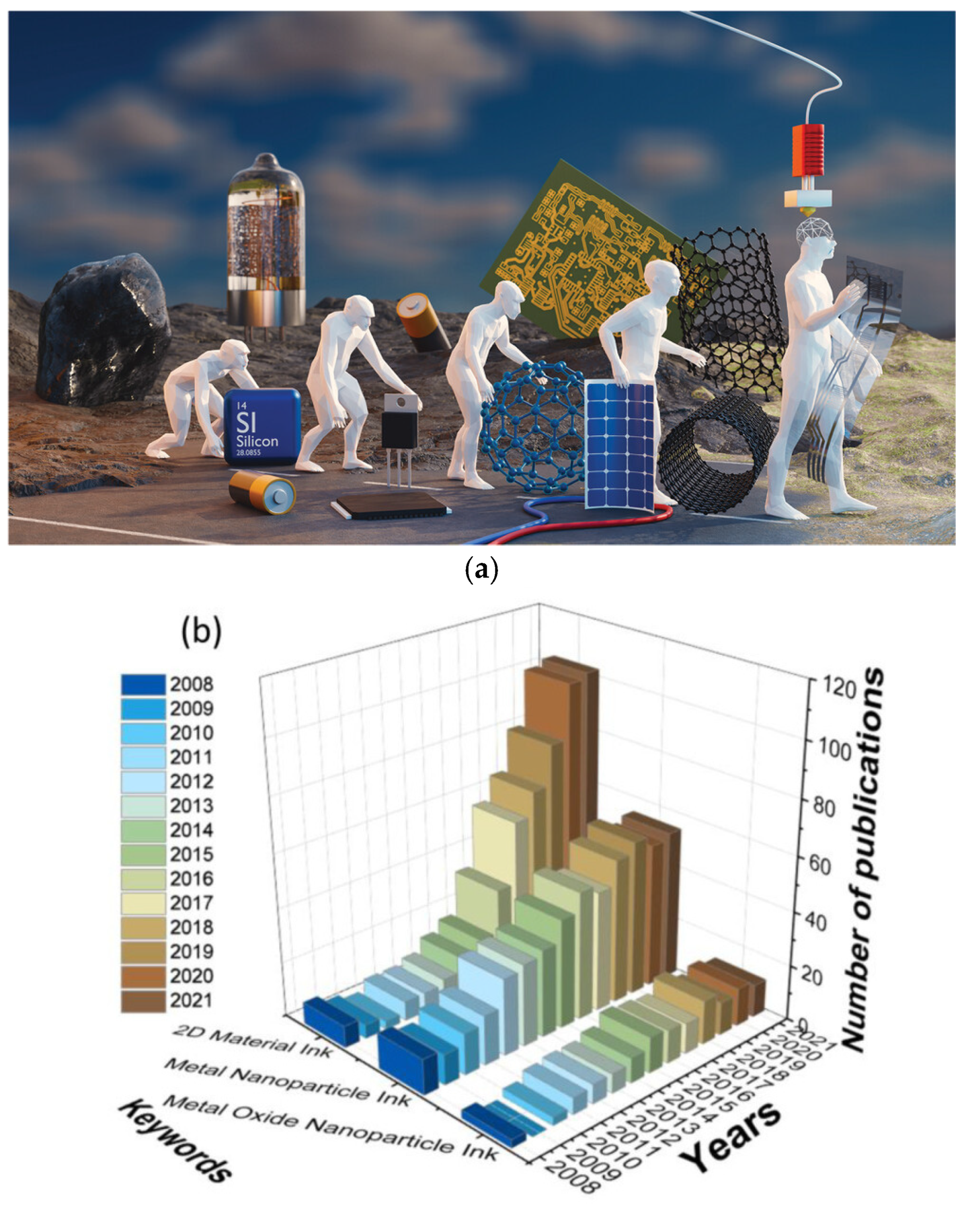
1. Introduction
1.1. Printing Electronics
1.2. Additive Manufacturing of Electronics
1.3. AI Automation
1.4. Outline of This Review
2. Printing Electronics
2.1. Research Trends
2.2. Contact Printing
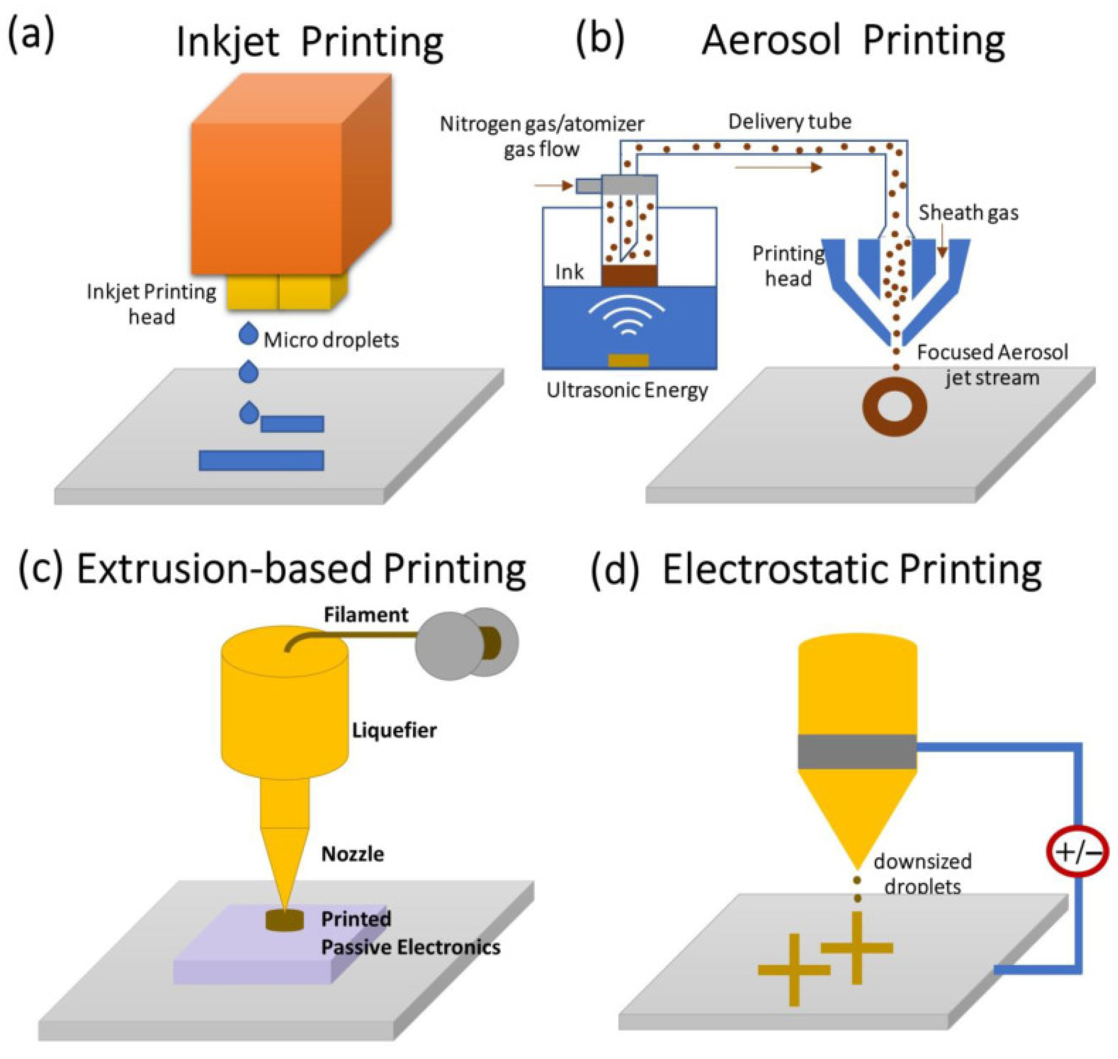
2.3. Non-Contact Printing: Main Techniques
2.4. Non-Contact Printing: Electrostatic Printing and Electrospinning
2.5. Opportunities and Challenges
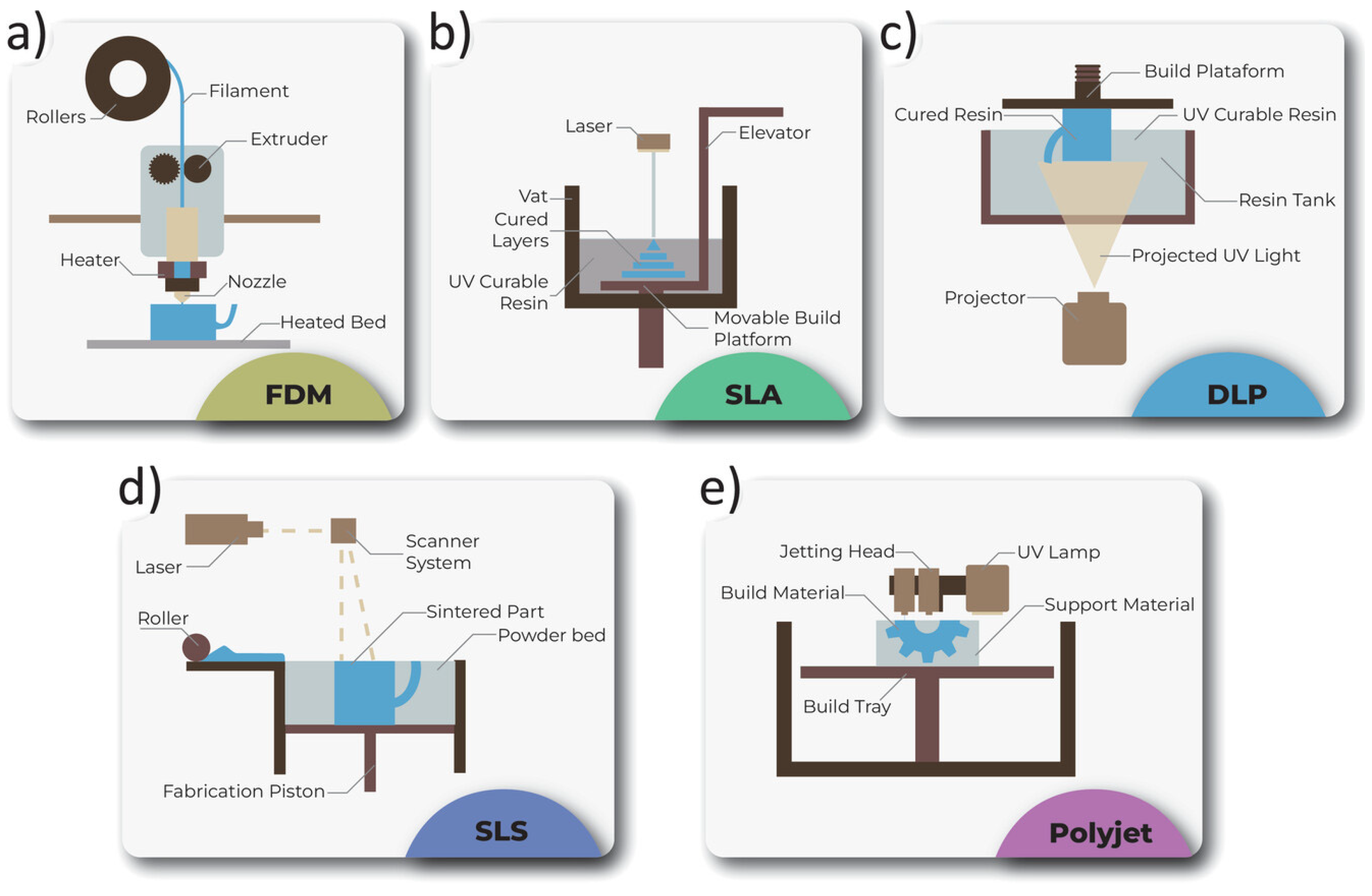
3. Three-Dimensional Printing of Electronics
3.1. Developments in 3D Printed Electronics
3.2. Supercapacitors by 3D Printing
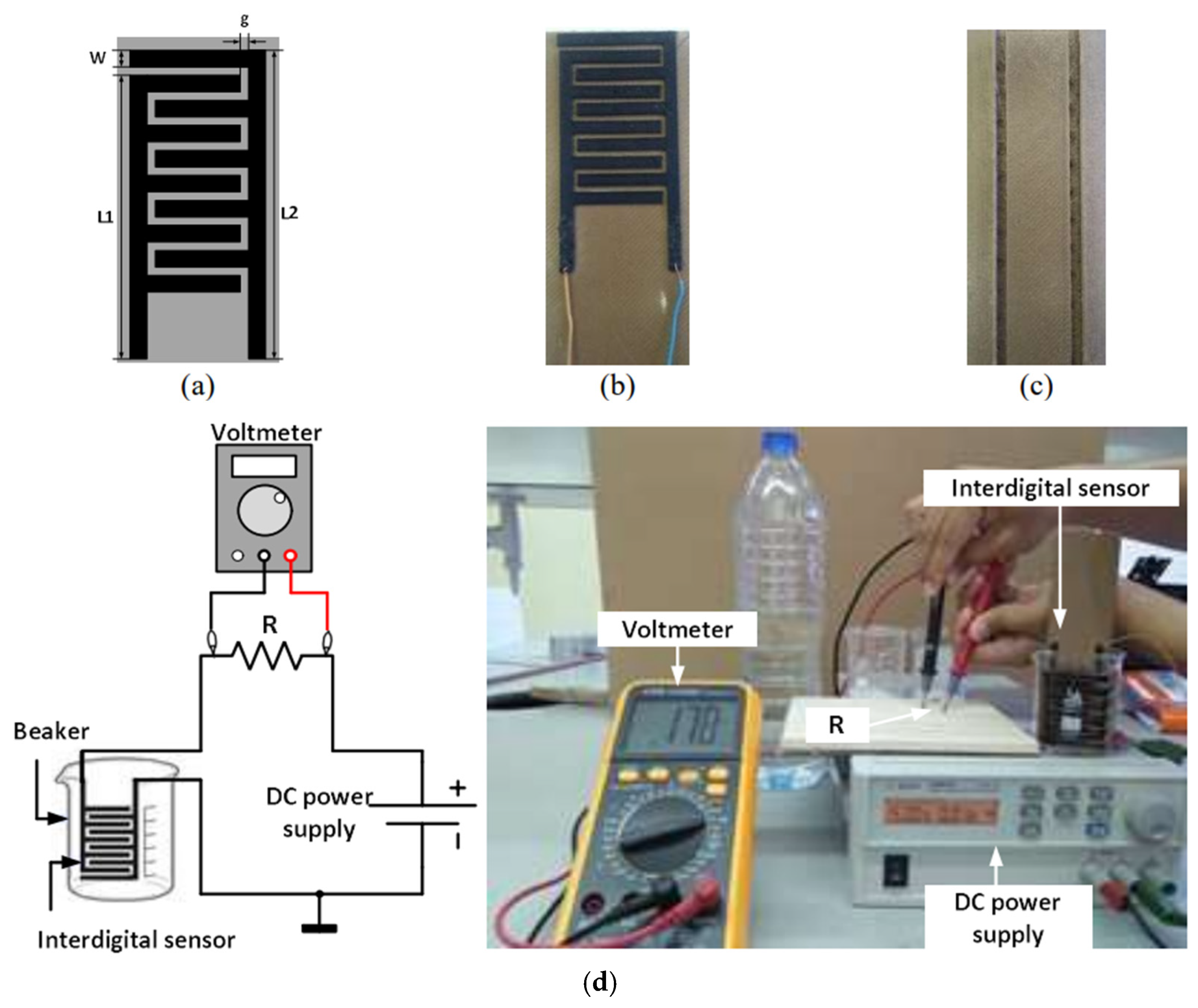
3.3. Sensors by 3D Printing
3.4. Batteries by 3D Printing
3.5. Fuel Cells by 3D Printing
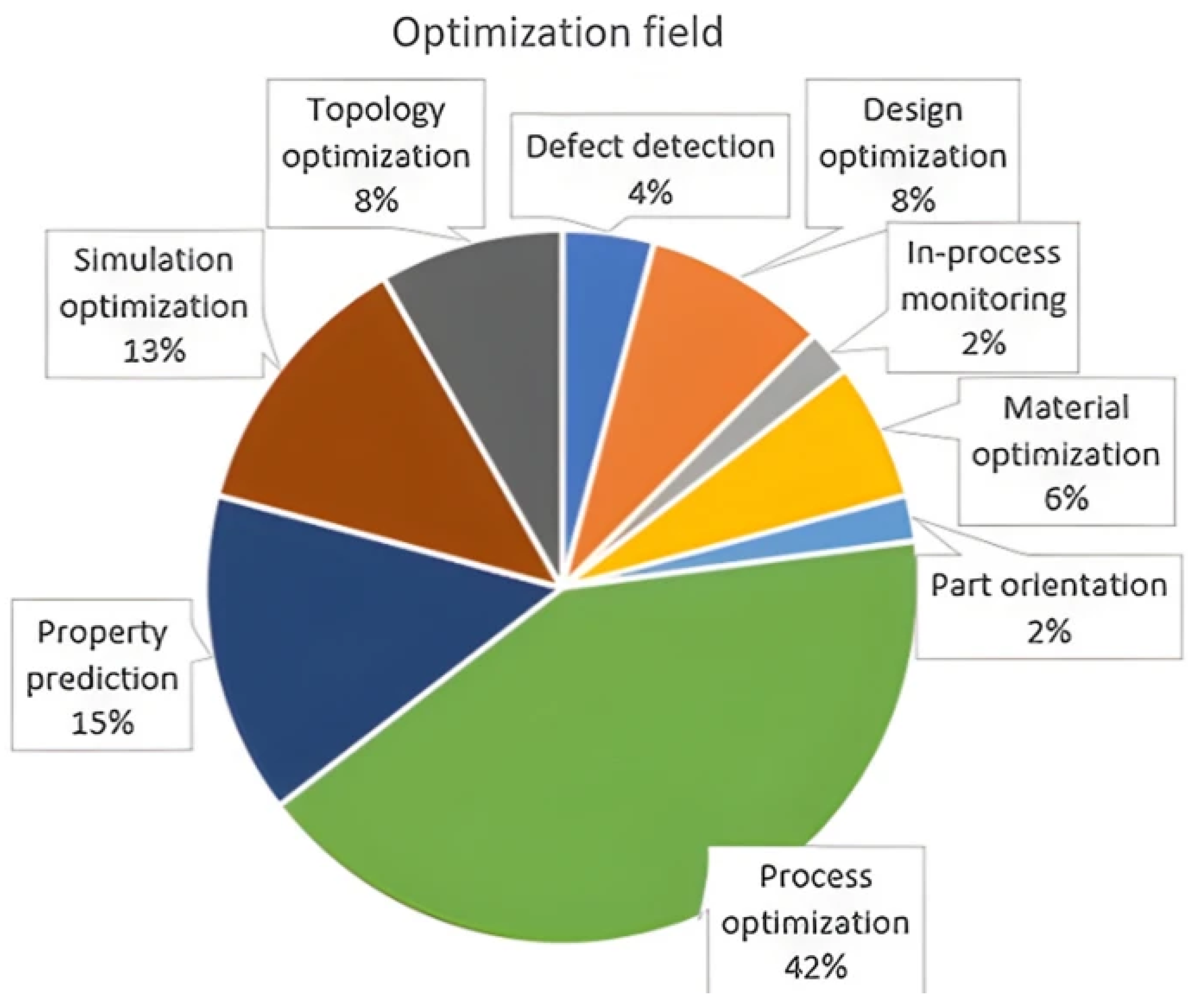
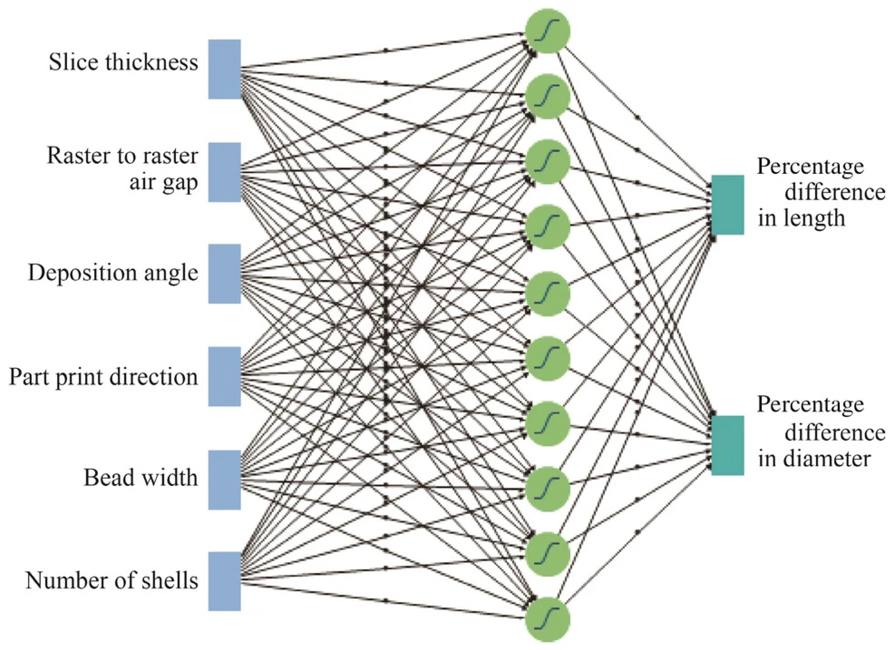
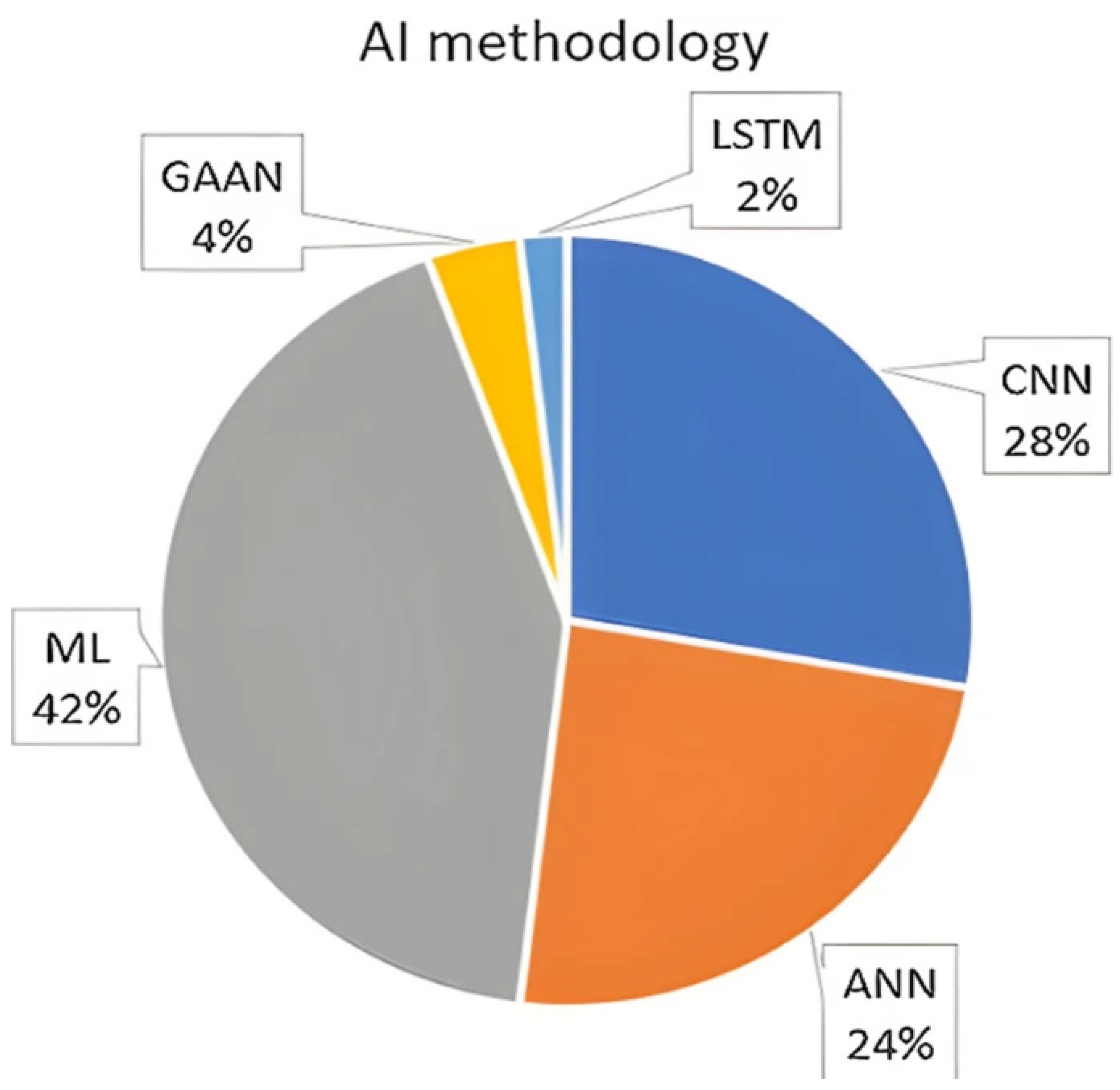
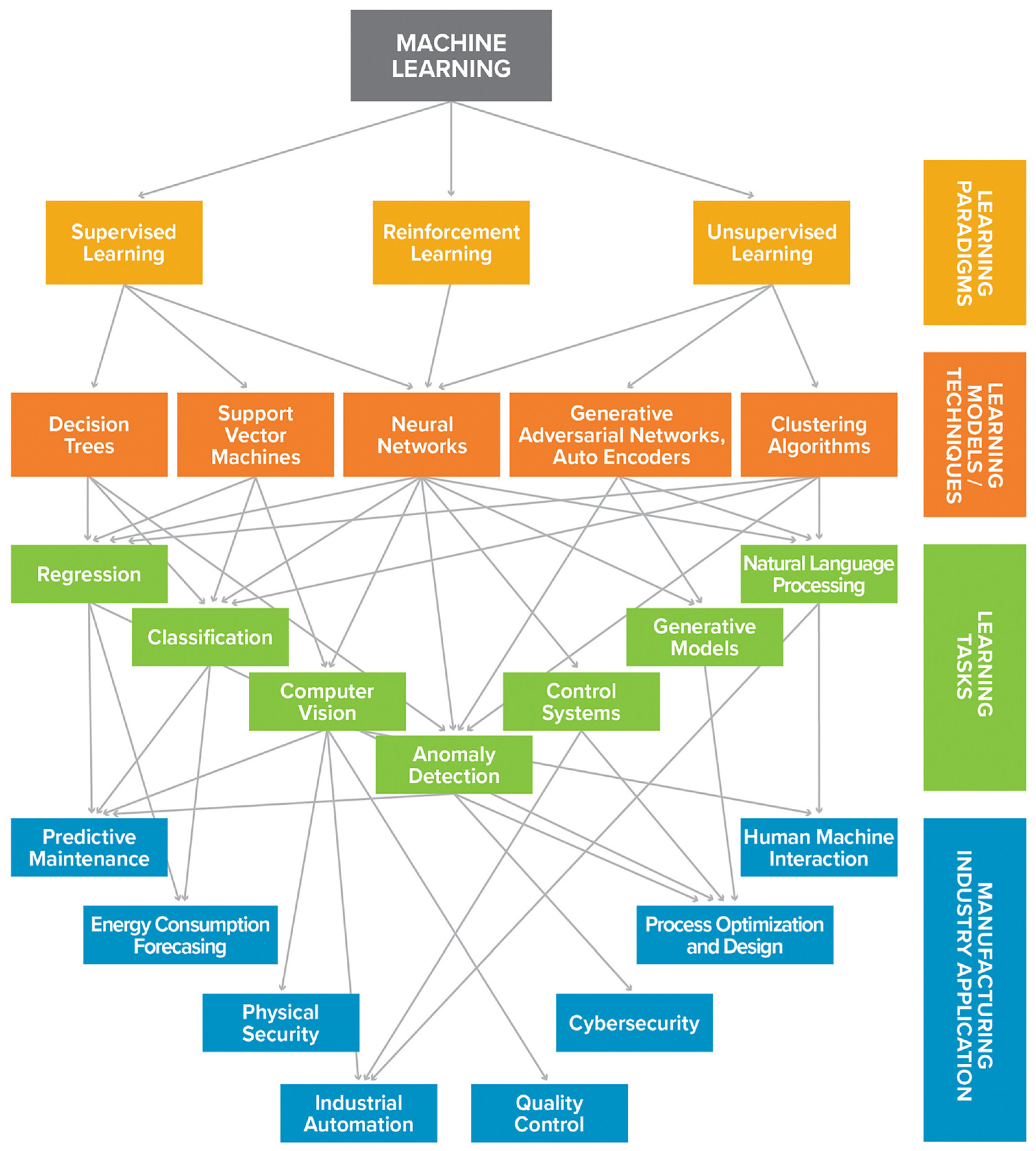
4. AI in 3D and Electronics Printing
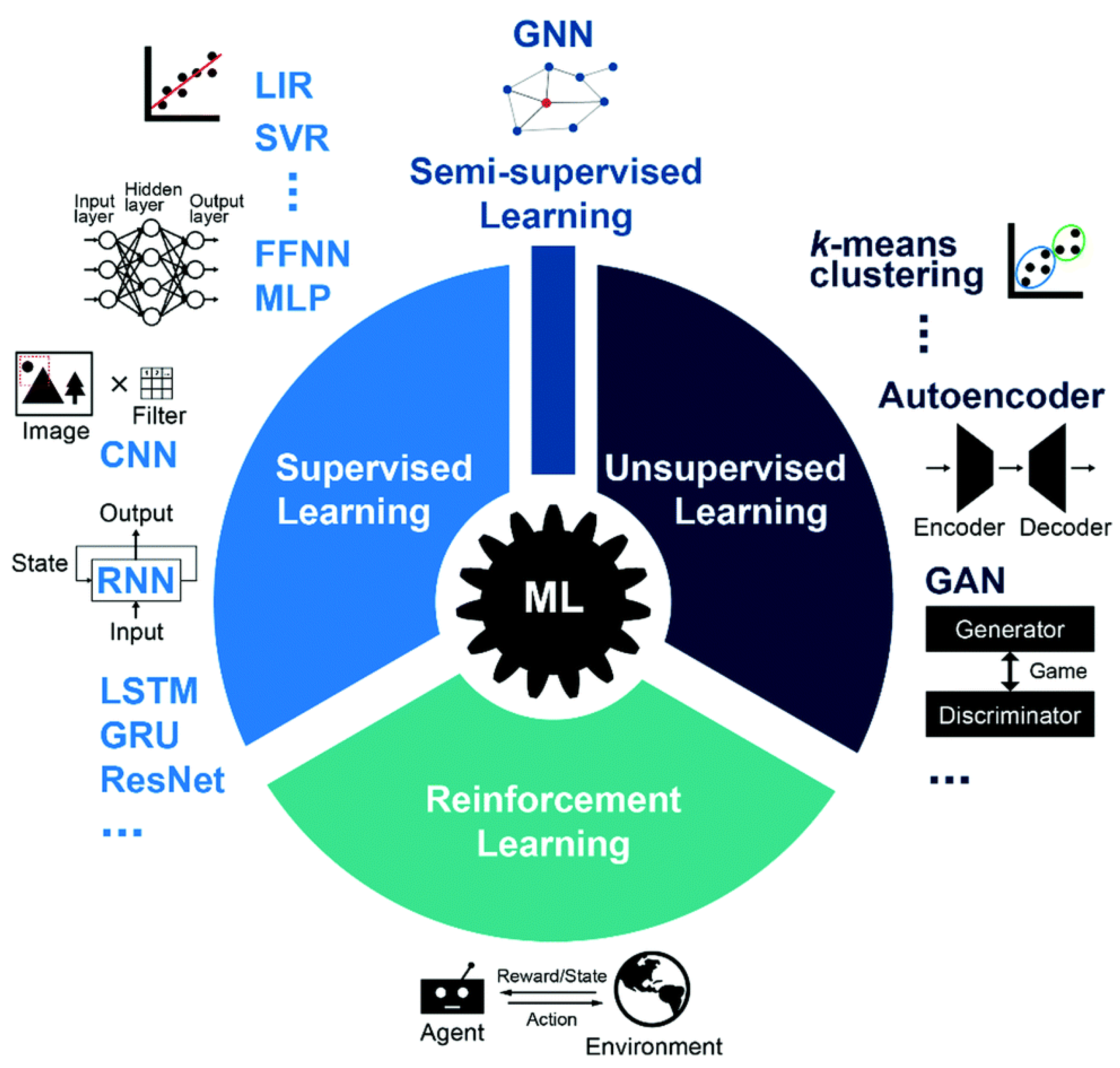
4.1. The Rise of AI
4.2. AI Applications
- (1)
- Inkjet path optimization
- (2)
- Defect prediction
- (3)
- Parameter reverse inference
4.3. Champion Models
4.4. Optimizing Property and Process Simultaneously
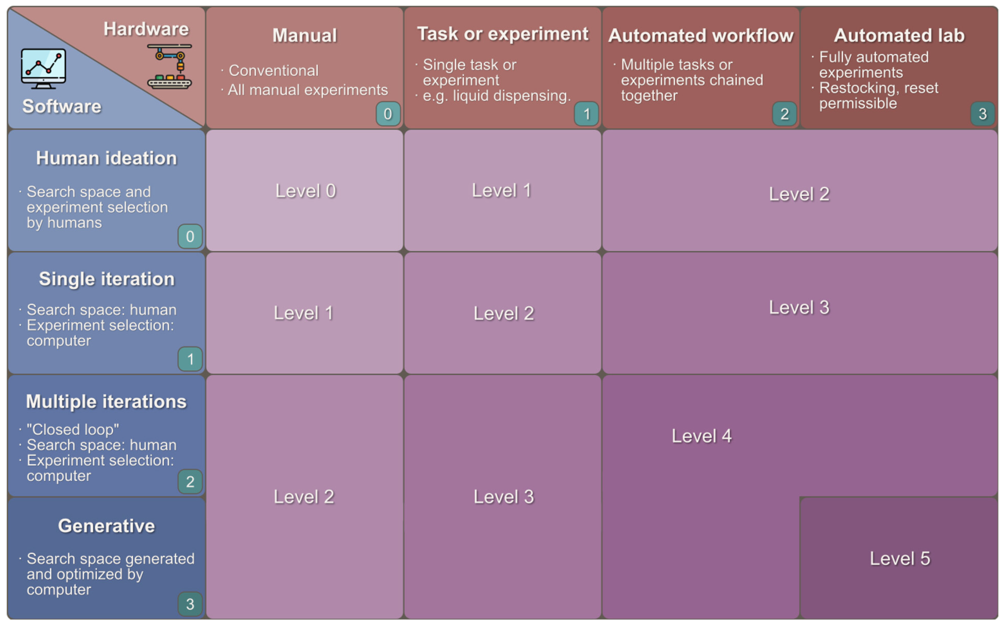
4.5. Levels of Automation
4.6. Possibilities
5. The Future of AI-Aided Electronics Printing
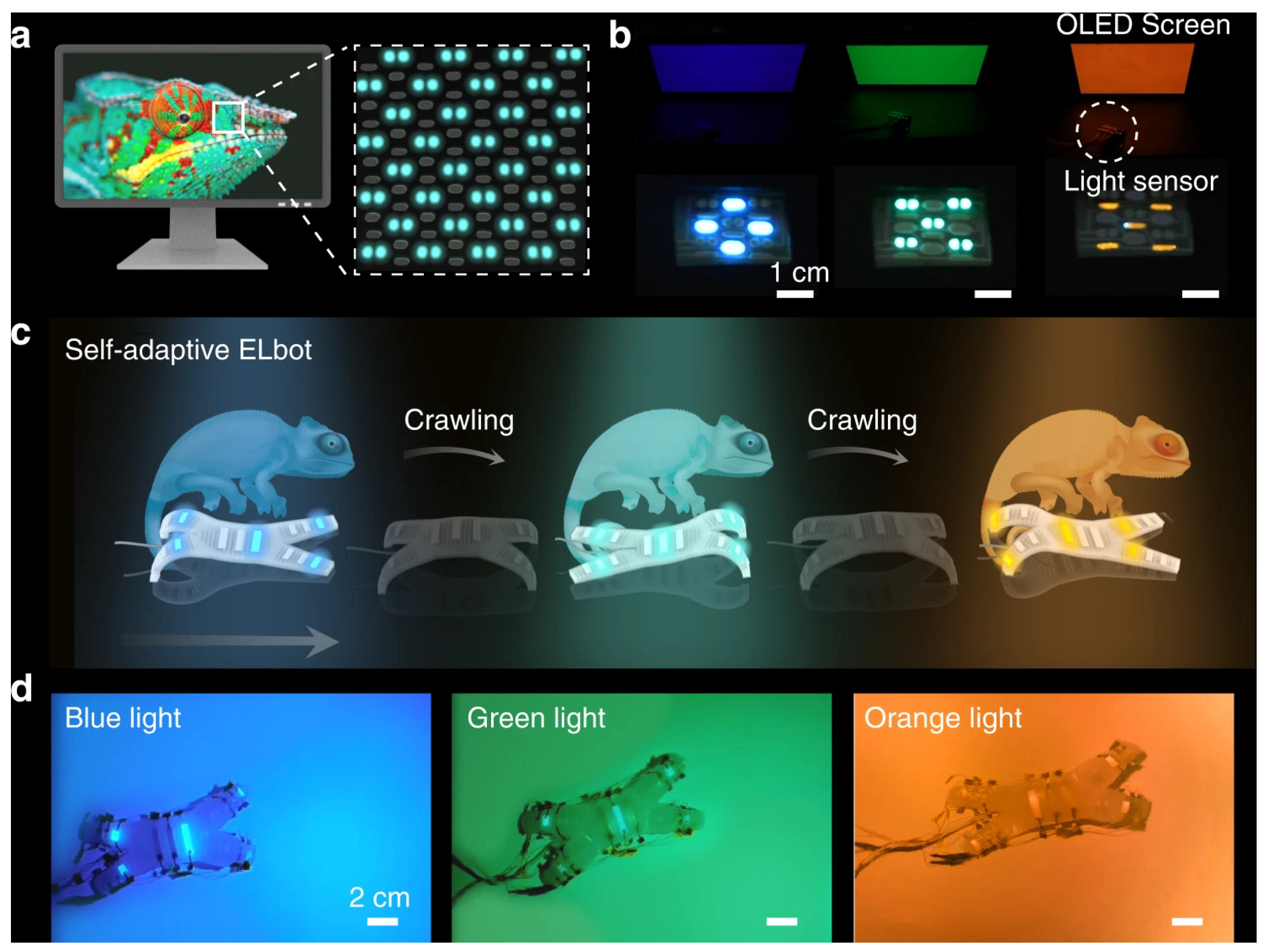
5.1. Recent Examples: Soft Robotics and Wearable Electronics
5.2. High Throughput Experimentations
5.3. Environmental Considerations
5.4. Conclusions
- Traditional techniques of electronics printing provide contact and non-contact pattern transferring to fabricate flexible electronics with low-cost, low-temperature processes.
- Additive manufacturing of electronics offers opportunities for multi-material, multi-process, personalized fabrication of sensors, electronics, energy storage, and harvest devices, which are not easily accomplishable by traditional ways of electronics printing.
- AI and algorithm-based optimization vastly improve the efficiency of 3D printing and electronics printing via a high-quality database, digital twin building, and process optimization.
Author Contributions
Funding
Acknowledgments
Conflicts of Interest
References
- Martins, P.; Pereira, N.; Lima, A.C.; Garcia, A.; Mendes-Filipe, C.; Policia, R.; Correia, V.; Lanceros-Mendez, S. Advances in Printing and Electronics: From Engagement to Commitment. Adv. Funct. Mater. 2023, 33, 2213744. [Google Scholar] [CrossRef]
- Lyu, Z.; Lim, G.J.H.; Koh, J.J.; Li, Y.; Ma, Y.; Ding, J.; Wang, J.; Hu, Z.; Wang, J.; Chen, W.; et al. Design and Manufacture of 3D-Printed Batteries. Joule 2021, 5, 89–114. [Google Scholar] [CrossRef]
- Goh, G.D.; Sing, S.L.; Yeong, W.Y. A Review on Machine Learning in 3D Printing: Applications, Potential, and Challenges. Artif. Intell. Rev. 2021, 54, 63–94. [Google Scholar] [CrossRef]
- Chandrasekaran, S.; Jayakumar, A.; Velu, R. A Comprehensive Review on Printed Electronics: A Technology Drift towards a Sustainable Future. Nanomaterials 2022, 12, 4251. [Google Scholar] [CrossRef]
- Zhou, L.; Miller, J.; Vezza, J.; Mayster, M.; Raffay, M.; Justice, Q.; Al Tamimi, Z.; Hansotte, G.; Sunkara, L.D.; Bernat, J. Additive Manufacturing: A Comprehensive Review. Sensors 2024, 24, 2668. [Google Scholar] [CrossRef]
- Dizon, J.R.C.; Gache, C.C.L.; Cascolan, H.M.S.; Cancino, L.T.; Advincula, R.C. Post-Processing of 3D-Printed Polymers. Technologies 2021, 9, 61. [Google Scholar] [CrossRef]
- Zhang, X.; Chu, D.; Zhao, X.; Gao, C.; Lu, L.; He, Y.; Bai, W. Machine Learning-Driven 3D Printing: A Review. Appl. Mater. Today 2024, 39, 102306. [Google Scholar] [CrossRef]
- Meng, L.; McWilliams, B.; Jarosinski, W.; Park, H.-Y.; Jung, Y.-G.; Lee, J.; Zhang, J. Machine Learning in Additive Manufacturing: A Review. JOM 2020, 72, 2363–2377. [Google Scholar] [CrossRef]
- Deed—Attribution-NonCommercial 4.0 International—Creative Commons. Available online: https://creativecommons.org/licenses/by-nc/4.0/ (accessed on 17 May 2025).
- Deed—Attribution 4.0 International—Creative Commons. Available online: https://creativecommons.org/licenses/by/4.0/ (accessed on 9 December 2024).
- Soum, V.; Cheong, H.; Kim, K.; Kim, Y.; Chuong, M.; Ryu, S.R.; Yuen, P.K.; Kwon, O.-S.; Shin, K. Programmable Contact Printing Using Ballpoint Pens with a Digital Plotter for Patterning Electrodes on Paper. ACS Omega 2018, 3, 16866–16873. [Google Scholar] [CrossRef]
- Dahiya, A.S.; Christou, A.; Neto, J.; Zumeit, A.; Shakthivel, D.; Dahiya, R. In Tandem Contact-Transfer Printing for High-Performance Transient Electronics. Adv. Electron. Mater. 2022, 8, 2200170. [Google Scholar] [CrossRef]
- Mechael, S.S.; D’Amaral, G.M.; Carmichael, T.B. Debossed Contact Printing as a Patterning Method for Paper-Based Electronics. ACS Appl. Mater. Interfaces 2023, 15, 44422–44432. [Google Scholar] [CrossRef] [PubMed]
- Christou, A.; Liu, F.; Dahiya, R. Development of a Highly Controlled System for Large-Area, Directional Printing of Quasi-1D Nanomaterials. Microsyst. Nanoeng. 2021, 7, 1–12. [Google Scholar] [CrossRef]
- Wiklund, J.; Karakoç, A.; Palko, T.; Yiğitler, H.; Ruttik, K.; Jäntti, R.; Paltakari, J. A Review on Printed Electronics: Fabrication Methods, Inks, Substrates, Applications and Environmental Impacts. J. Manuf. Mater. Process. 2021, 5, 89. [Google Scholar] [CrossRef]
- Bi, S.; Gao, B.; Han, X.; He, Z.; Metts, J.; Jiang, C.; Asare-Yeboah, K. Recent Progress in Printing Flexible Electronics: A Review. Sci. China Technol. Sci. 2024, 67, 2363–2386. [Google Scholar] [CrossRef]
- Kumar, A.; Whitesides, G.M. Features of Gold Having Micrometer to Centimeter Dimensions Can Be Formed through a Combination of Stamping with an Elastomeric Stamp and an Alkanethiol ‘“Ink”’ Followed by Chemical Etching. Appl. Phys. Lett. 1993, 63, 2002–2004. [Google Scholar] [CrossRef]
- Meitl, M.A.; Zhu, Z.-T.; Kumar, V.; Lee, K.J.; Feng, X.; Huang, Y.Y.; Adesida, I.; Nuzzo, R.G.; Rogers, J.A. Transfer Printing by Kinetic Control of Adhesion to an Elastomeric Stamp. Nat. Mater. 2006, 5, 33–38. [Google Scholar] [CrossRef]
- Chou, S.Y.; Krauss, P.R.; Renstrom, P.J. Nanoimprint Lithography. J. Vac. Sci. Technol. B Microelectron. Nanometer Struct. Process. Meas. Phenom. 1996, 14, 4129–4133. [Google Scholar] [CrossRef]
- Wu, W. Introduction to Printed Electronics. In Printed Electronics Technologies; Royal Society of Chemistry: London, UK, 2022. [Google Scholar] [CrossRef]
- Xu, Y.; Schwab, M.G.; Strudwick, A.J.; Hennig, I.; Feng, X.; Wu, Z.; Müllen, K. Screen-Printable Thin Film Supercapacitor Device Utilizing Graphene/Polyaniline Inks. Adv. Energy Mater. 2013, 3. Available online: https://advanced.onlinelibrary.wiley.com/doi/10.1002/aenm.201300184 (accessed on 18 May 2025). [CrossRef]
- Liu, Z.; Tian, B.; Zhang, B.; Zhang, Z.; Liu, J.; Zhao, L.; Shi, P.; Lin, Q.; Jiang, Z. High-Performance Temperature Sensor by Employing Screen Printing Technology. Micromachines 2021, 12, 924. [Google Scholar] [CrossRef]
- Liu, Z.; Tian, B.; Jiang, Z.; Li, S.; Lei, J.; Zhang, Z.; Liu, J.; Shi, P.; Lin, Q. Flexible Temperature Sensor with High Sensitivity Ranging from Liquid Nitrogen Temperature to 1200 °C. Int. J. Extreme Manuf. 2022, 5, 015601. [Google Scholar] [CrossRef]
- Beedasy, V.; Smith, P.J. Printed Electronics as Prepared by Inkjet Printing. Materials 2020, 13, 704. [Google Scholar] [CrossRef] [PubMed]
- Kaçar, R.; Serin, R.B.; Uçar, E.; Ülkü, A. A Review of High-End Display Technologies Focusing on Inkjet Printed Manufacturing. Mater. Today Commun. 2023, 35, 105534. [Google Scholar] [CrossRef]
- Azad, B.K.D.; Roozbahani, A.; Tabatabaei, S.M.; Valinejad, A.; Fazelian, A.; Shahmoradi, K.; Khatami, F.; Aghamir, S.M.K.; Kolahdouz, M. Inkjet-Printed Electronics for Rapid and Low-Cost Prototyping of Digital Microfluidic Devices Using an off-the-Shelf Printer. Sci. Rep. 2025, 15, 4578. [Google Scholar] [CrossRef]
- Lian, H.; Qi, L.; Luo, J.; Zhang, R.; Niu, J. Direct Printing of Graphene Terahertz Closed-Ring Resonator Array from Periodic Single Droplets via Enhanced Coffee-Ring Effect. Carbon 2023, 215, 118485. [Google Scholar] [CrossRef]
- Niu, J.; Qi, L.; Lian, H.; Luo, J.; Zhang, R.; Chao, X. Revisiting the Inhomogeneity in Drop-on-Demand Printing of Graphene: An Effective Route for Overcoming the Coffee-Ring Effect. Surf. Interfaces 2024, 46, 104036. [Google Scholar] [CrossRef]
- Lei, J.; Tian, B.; Liu, X.; Wang, M.; Li, L.; Liu, Z.; Liu, J.; Zhang, Z.; Shi, M.; Tan, Q.; et al. High Temperature Resistant Thin Film Thermocouple Prepared Based on Inkjet Printing. Ceram. Int. 2025, 51, 4613–4622. [Google Scholar] [CrossRef]
- Li, X.; Chen, W.; Qian, Q.; Huang, H.; Chen, Y.; Wang, Z.; Chen, Q.; Yang, J.; Li, J.; Mai, Y. Electrospinning-Based Strategies for Battery Materials. Adv. Energy Mater. 2021, 11, 2000845. [Google Scholar] [CrossRef]
- Joshi, B.; Samuel, E.; Kim, Y.; Yarin, A.L.; Swihart, M.T.; Yoon, S.S. Progress and Potential of Electrospinning-Derived Substrate-Free and Binder-Free Lithium-Ion Battery Electrodes. Chem. Eng. J. 2022, 430, 132876. [Google Scholar] [CrossRef]
- Senthilkumar, S.H.; Ramasubramanian, B.; Rao, R.P.; Chellappan, V.; Ramakrishna, S. Advances in Electrospun Materials and Methods for Li-Ion Batteries. Polymers 2023, 15, 1622. [Google Scholar] [CrossRef]
- Wang, Y.; Liu, Y.; Liu, Y.; Shen, Q.; Chen, C.; Qiu, F.; Li, P.; Jiao, L.; Qu, X. Recent Advances in Electrospun Electrode Materials for Sodium-Ion Batteries. J. Energy Chem. 2021, 54, 225–241. [Google Scholar] [CrossRef]
- Galliker, P.; Schneider, J.; Eghlidi, H.; Kress, S.; Sandoghdar, V.; Poulikakos, D. Direct Printing of Nanostructures by Electrostatic Autofocussing of Ink Nanodroplets. Nat. Commun. 2012, 3, 890. [Google Scholar] [CrossRef] [PubMed]
- Wang, Y.; Yokota, T.; Someya, T. Electrospun Nanofiber-Based Soft Electronics. NPG Asia Mater. 2021, 13, 1–22. [Google Scholar] [CrossRef]
- Karatay, O.; Dogan, M. Modelling of Electrospinning Process at Various Electric Fields. Micro Nano Lett. 2011, 6, 858–862. [Google Scholar] [CrossRef]
- Tucker, N.; Stanger, J.J.; Staiger, M.P.; Razzaq, H.; Hofman, K. The History of the Science and Technology of Electrospinning from 1600 to 1995. J. Eng. Fibers Fabr. 2012, 7 (Suppl. S2), 155892501200702S10. [Google Scholar] [CrossRef]
- Tan, H.W.; Choong, Y.Y.C.; Kuo, C.N.; Low, H.Y.; Chua, C.K. 3D Printed Electronics: Processes, Materials and Future Trends. Prog. Mater. Sci. 2022, 127, 100945. [Google Scholar] [CrossRef]
- Rao, C.H.; Avinash, K.; Varaprasad, B.K.S.V.L.; Goel, S. A Review on Printed Electronics with Digital 3D Printing: Fabrication Techniques, Materials, Challenges and Future Opportunities. J. Electron. Mater. 2022, 51, 2747–2765. [Google Scholar] [CrossRef]
- Goh, G.L.; Zhang, H.; Chong, T.H.; Yeong, W.Y. 3D Printing of Multilayered and Multimaterial Electronics: A Review. Adv. Electron. Mater. 2021, 7, 2100445. [Google Scholar] [CrossRef]
- Hua, W.; Mitchell, K.; Kariyawasam, L.S.; Do, C.; Chen, J.; Raymond, L.; Valentin, N.; Coulter, R.; Yang, Y.; Jin, Y. Three-Dimensional Printing in Stimuli-Responsive Yield-Stress Fluid with an Interactive Dual Microstructure. ACS Appl. Mater. Interfaces 2022, 14, 39420–39431. [Google Scholar] [CrossRef]
- Kharat, V.J.; Singh, P.; Sharath Raju, G.; Kumar Yadav, D.; Satyanarayana Gupta, M.; Arun, V.; Hussein Majeed, A.; Singh, N. Additive Manufacturing (3D Printing): A Review of Materials, Methods, Applications and Challenges. Mater. Today Proc. 2023; in press. [Google Scholar] [CrossRef]
- Persad, J.; Rocke, S. Multi-Material 3D Printed Electronic Assemblies: A Review. Results Eng. 2022, 16, 100730. [Google Scholar] [CrossRef]
- Persad, J.; Rocke, S. A Survey of 3D Printing Technologies as Applied to Printed Electronics. IEEE Access 2022, 10, 27289–27319. [Google Scholar] [CrossRef]
- Park, Y.-G.; Yun, I.; Chung, W.G.; Park, W.; Lee, D.H.; Park, J.-U. High-Resolution 3D Printing for Electronics. Adv. Sci. 2022, 9, 2104623. [Google Scholar] [CrossRef] [PubMed]
- Zhan, S.; Guo, A.X.Y.; Cao, S.C.; Liu, N. 3D Printing Soft Matters and Applications: A Review. Int. J. Mol. Sci. 2022, 23, 3790. [Google Scholar] [CrossRef] [PubMed]
- Espera, A.H.; Dizon, J.R.C.; Valino, A.D.; Advincula, R.C. Advancing Flexible Electronics and Additive Manufacturing. Jpn. J. Appl. Phys. 2022, 61, SE0803. [Google Scholar] [CrossRef]
- Kwon, K.-S.; Rahman, M.K.; Phung, T.H.; Hoath, S.D.; Jeong, S.; Kim, J.S. Review of Digital Printing Technologies for Electronic Materials. Flex. Print. Electron. 2020, 5, 043003. [Google Scholar] [CrossRef]
- Kiranlal, S.; Brathikan, V.M.; Anandh, B.; Vikash, S. A Review on Electrical and Electronics Part of 3D Printer. IOP Conf. Ser. Mater. Sci. Eng. 2022, 1228, 012007. [Google Scholar] [CrossRef]
- Cost Comparison of 3D Printing Methods: SLS and More. Available online: https://www.zongheng3d.com/cost-comparison-of-3d-printing-methods-sls-vs-others/ (accessed on 22 May 2025).
- Ngo, T.D.; Kashani, A.; Imbalzano, G.; Nguyen, K.T.Q.; Hui, D. Additive Manufacturing (3D Printing): A Review of Materials, Methods, Applications and Challenges. Compos. Part B Eng. 2018, 143, 172–196. [Google Scholar] [CrossRef]
- Gibson, I.; Rosen, D.; Stucker, B.; Khorasani, M. Additive Manufacturing Technologies; Springer International Publishing: Cham, Switzerland, 2021. [Google Scholar] [CrossRef]
- Berman, B. 3-D Printing: The New Industrial Revolution. Bus. Horiz. 2012, 55, 155–162. [Google Scholar] [CrossRef]
- Iftekar, S.F.; Aabid, A.; Amir, A.; Baig, M. Advancements and Limitations in 3D Printing Materials and Technologies: A Critical Review. Polymers 2023, 15, 2519. [Google Scholar] [CrossRef]
- Rezaei, F.; Carlsson, D.O.; Hedin Dahlstrom, J.; Lindh, J.; Johansson, S. Direct Ink Writing of High-Resolution Cellulose Structures. Sci. Rep. 2023, 13, 22044. [Google Scholar] [CrossRef]
- Costa, C.M.; Gonçalves, R.; Lanceros-Méndez, S. Recent Advances and Future Challenges in Printed Batteries. Energy Storage Mater. 2020, 28, 216–234. [Google Scholar] [CrossRef]
- Zhang, F.; Wei, M.; Viswanathan, V.V.; Swart, B.; Shao, Y.; Wu, G.; Zhou, C. 3D Printing Technologies for Electrochemical Energy Storage. Nano Energy 2017, 40, 418–431. [Google Scholar] [CrossRef]
- Fu, K.; Yao, Y.; Dai, J.; Hu, L. Progress in 3D Printing of Carbon Materials for Energy-Related Applications. Adv. Mater. 2017, 29, 1603486. [Google Scholar] [CrossRef] [PubMed]
- Zhang, Y.-Z.; Wang, Y.; Cheng, T.; Yao, L.-Q.; Li, X.; Lai, W.-Y.; Huang, W. Printed Supercapacitors: Materials, Printing and Applications. Chem. Soc. Rev. 2019, 48, 3229–3264. [Google Scholar] [CrossRef]
- Choi, K.-H.; Yoo, J.; Lee, C.K.; Lee, S.-Y. All-Inkjet-Printed, Solid-State Flexible Supercapacitors on Paper. Energy Environ. Sci. 2016, 9, 2812–2821. [Google Scholar] [CrossRef]
- Mevada, C.; Tissari, J.; Parihar, V.S.; Tewari, A.; Keskinen, J.; Mäntysalo, M. Bio-Inspired 3D-Printed Supercapacitors for Sustainable Energy Storage. J. Power Sources 2024, 624, 235529. [Google Scholar] [CrossRef]
- Li, M.; Zhou, S.; Cheng, L.; Mo, F.; Chen, L.; Yu, S.; Wei, J. 3D Printed Supercapacitor: Techniques, Materials, Designs, and Applications. Adv. Funct. Mater. 2023, 33, 2208034. [Google Scholar] [CrossRef]
- Zhang, N.; Wang, Z.; Zhao, Z.; Zhang, D.; Feng, J.; Yu, L.; Lin, Z.; Guo, Q.; Huang, J.; Mao, J.; et al. 3D Printing of Micro-Nano Devices and Their Applications. Microsyst. Nanoeng. 2025, 11, 1–23. [Google Scholar] [CrossRef]
- Lee, J.; So, H. 3D-Printing-Assisted Flexible Pressure Sensor with a Concentric Circle Pattern and High Sensitivity for Health Monitoring. Microsyst. Nanoeng. 2023, 9, 1–12. [Google Scholar] [CrossRef]
- Hassan, M.S.; Zaman, S.; Dantzler, J.Z.R.; Leyva, D.H.; Mahmud, M.S.; Ramirez, J.M.; Gomez, S.G.; Lin, Y. 3D Printed Integrated Sensors: From Fabrication to Applications—A Review. Nanomaterials 2023, 13, 3148. [Google Scholar] [CrossRef]
- Han, T.; Kundu, S.; Nag, A.; Xu, Y. 3D Printed Sensors for Biomedical Applications: A Review. Sensors 2019, 19, 1706. [Google Scholar] [CrossRef]
- Pan, L.; Zhou, S.; Yang, J.; Fei, T.; Mao, S.; Fu, L.; Lin, C.-T. 3D-Printed Electrodes for Electrochemical Detection of Environmental Analytes. Anal. Methods 2025, 17, 2235–2253. [Google Scholar] [CrossRef] [PubMed]
- Ali, M.A.; Hu, C.; Yttri, E.A.; Panat, R. Recent Advances in 3D Printing of Biomedical Sensing Devices. Adv. Funct. Mater. 2022, 32, 2107671. [Google Scholar] [CrossRef] [PubMed]
- Wolstrup, A.F.; Spangenberg, J.; Yamamoto, A.; Gleadall, A.; Zsurzsan, G. Advances in 3D Printed Electromechanical Sensors: Performance Comparison, Trends, and Future Directions. Addit. Manuf. 2025, 106, 104799. [Google Scholar] [CrossRef]
- Liang, X.; Zhang, M.; Chong, C.-M.; Lin, D.; Chen, S.; Zhen, Y.; Ding, H.; Zhong, H.-J. Recent Advances in the 3D Printing of Conductive Hydrogels for Sensor Applications: A Review. Polymers 2024, 16, 2131. [Google Scholar] [CrossRef]
- Jin, Y.; Xue, S.; He, Y. Flexible Pressure Sensors Enhanced by 3D-Printed Microstructures. Adv. Mater. 2025, e2500076. [Google Scholar] [CrossRef]
- Khan, Y.; Thielens, A.; Muin, S.; Ting, J.; Baumbauer, C.; Arias, A.C. A New Frontier of Printed Electronics: Flexible Hybrid Electronics. Adv. Mater. 2020, 32, 1905279. [Google Scholar] [CrossRef]
- Wang, X.; Zhang, M.; Zhang, L.; Xu, J.; Xiao, X.; Zhang, X. Inkjet-Printed Flexible Sensors: From Function Materials, Manufacture Process, and Applications Perspective. Mater. Today Commun. 2022, 31, 103263. [Google Scholar] [CrossRef]
- Ponan, W.; Harnsoongnoen, S. 3D Printing of Interdigital Sensor Based Conductive ABS for Salt and Sucrose Concentration Sensing. J. Phys. Conf. Ser. 2019, 1380, 012129. [Google Scholar] [CrossRef]
- Deed—Attribution 3.0 Unported—Creative Commons. Available online: https://creativecommons.org/licenses/by/3.0/ (accessed on 9 December 2024).
- Mouraliraman, D.; Thiagarajan, A.; Deepa, S.; Sriram, G.; Aruchamy, K.; Oh, T.H.; Shin, D. 3D Printed Lithium-Ion Batteries: An in-Depth Examination of the Advancements in Flexibility and Stand-Alone Capability. J. Energy Storage 2024, 81, 110395. [Google Scholar] [CrossRef]
- Fonseca, N.; Thummalapalli, S.V.; Jambhulkar, S.; Ravichandran, D.; Zhu, Y.; Patil, D.; Thippanna, V.; Ramanathan, A.; Xu, W.; Guo, S.; et al. 3D Printing-Enabled Design and Manufacturing Strategies for Batteries: A Review. Small 2023, 19, 2302718. [Google Scholar] [CrossRef]
- Gao, X.; Liu, K.; Su, C.; Zhang, W.; Dai, Y.; Parkin, I.P.; Carmalt, C.J.; He, G. From Bibliometric Analysis: 3D Printing Design Strategies and Battery Applications with a Focus on Zinc-Ion Batteries. SmartMat 2024, 5, e1197. [Google Scholar] [CrossRef]
- Reyes, C.; Somogyi, R.; Niu, S.; Cruz, M.A.; Yang, F.; Catenacci, M.J.; Rhodes, C.P.; Wiley, B.J. Three-Dimensional Printing of a Complete Lithium Ion Battery with Fused Filament Fabrication. ACS Appl. Energy Mater. 2018, 1, 5268–5279. [Google Scholar] [CrossRef]
- Mottaghi, M.; Pearce, J.M. A Review of 3D Printing Batteries. Batteries 2024, 10, 110. [Google Scholar] [CrossRef]
- Maurel, A.; Grugeon, S.; Fleutot, B.; Courty, M.; Prashantha, K.; Tortajada, H.; Armand, M.; Panier, S.; Dupont, L. Three-Dimensional Printing of a LiFePO4/Graphite Battery Cell via Fused Deposition Modeling. Sci. Rep. 2019, 9, 18031. [Google Scholar] [CrossRef]
- Ma, J.; Zheng, S.; Fu, Y.; Wang, X.; Qin, J.; Wu, Z.-S. The Status and Challenging Perspectives of 3D-Printed Micro-Batteries. Chem. Sci. 2024, 15, 5451–5481. [Google Scholar] [CrossRef]
- Maurel, A.; Pavone, A.; Stano, G.; Martinez, A.C.; MacDonald, E.; Percoco, G. Manufacturing-Oriented Review on 3D Printed Lithium-Ion Batteries Fabricated Using Material Extrusion. Virtual Phys. Prototyp. 2023, 18, e2264281. [Google Scholar] [CrossRef]
- Wu, J.; Xu, S. Manufacturing Flow Batteries Using Advanced 3D Printing Technology—A Review. Front. Chem. Eng. 2023, 5, 1144237. [Google Scholar] [CrossRef]
- Sun, K.; Wei, T.-S.; Ahn, B.Y.; Seo, J.Y.; Dillon, S.J.; Lewis, J.A. 3D Printing of Interdigitated Li-Ion Microbattery Architectures. Adv. Mater. 2013, 25, 4539–4543. [Google Scholar] [CrossRef]
- Wei, T.-S.; Ahn, B.Y.; Grotto, J.; Lewis, J.A. 3D Printing of Customized Li-Ion Batteries with Thick Electrodes. Adv. Mater. 2018, 30, 1703027. [Google Scholar] [CrossRef]
- Martinez, A.C.; Schiaffino, E.M.; Aranzola, A.P.; Fernandez, C.A.; Seol, M.-L.; Sherrard, C.G.; Jones, J.; Huddleston, W.H.; Dornbusch, D.A.; Sreenivasan, S.T.; et al. Multiprocess 3D Printing of Sodium-Ion Batteries via Vat Photopolymerization and Direct Ink Writing. J. Phys. Energy 2023, 5, 045010. [Google Scholar] [CrossRef]
- Ma, J.; Zheng, S.; Chi, L.; Liu, Y.; Zhang, Y.; Wang, K.; Wu, Z.-S. 3D Printing Flexible Sodium-Ion Microbatteries with Ultrahigh Areal Capacity and Robust Rate Capability. Adv. Mater. 2022, 34, 2205569. [Google Scholar] [CrossRef] [PubMed]
- Net Zero Roadmap: A Global Pathway to Keep the 1.5 °C Goal in Reach—Analysis. IEA. Available online: https://www.iea.org/reports/net-zero-roadmap-a-global-pathway-to-keep-the-15-0c-goal-in-reach (accessed on 9 January 2025).
- Morin, A.; Balestrière, P.; LaManna, J.M.; Baltic, E.; Hussey, D.S.; Jacobson, D.L.; Vacquier, C.; Poirot-Crouvezier, J.-P. Experimental and Modeling Analyses of the Correlation between Local 3D Heterogeneities and the Macroscopic Observers of a Proton Exchange Membrane Fuel Cell Stack. J. Electrochem. Soc. 2024, 171, 044508. [Google Scholar] [CrossRef]
- Lehmann, M.; Leonard, D.; Zheng, J.; He, L.; Tang, X.; Chen, X.C.; Lim, K.H.; Maurya, S.; Kim, Y.S.; Saito, T. Quaternized Polynorbornene Random Copolymers for Fuel Cell Devices. ACS Appl. Energy Mater. 2023, 6, 1822–1833. [Google Scholar] [CrossRef]
- Chabot, F.; Lee, J.; Vandenberghe, F.; Guétaz, L.; Gebel, G.; Lyonnard, S.; Porcar, L.; Rosini, S.; Morin, A. Detailed Catalyst Layer Structure of Proton Exchange Membrane Fuel Cells from Contrast Variation Small-Angle Neutron Scattering. ACS Appl. Energy Mater. 2023, 6, 1185–1196. [Google Scholar] [CrossRef]
- Cullen, D.A.; Neyerlin, K.C.; Ahluwalia, R.K.; Mukundan, R.; More, K.L.; Borup, R.L.; Weber, A.Z.; Myers, D.J.; Kusoglu, A. New Roads and Challenges for Fuel Cells in Heavy-Duty Transportation. Nat. Energy 2021, 6, 462–474. [Google Scholar] [CrossRef]
- Pesce, A.; Hornés, A.; Núñez, M.; Morata, A.; Torrell, M.; Tarancón, A. 3D Printing the next Generation of Enhanced Solid Oxide Fuel and Electrolysis Cells. J. Mater. Chem. A 2020, 8, 16926–16932. [Google Scholar] [CrossRef]
- Golubkov, S.S.; Morozova, S.M. Recent Progress of 3D Printing of Polymer Electrolyte Membrane-Based Fuel Cells for Clean Energy Generation. Polymers 2023, 15, 4553. [Google Scholar] [CrossRef]
- Lira, M.; Kostretsova, N.; Babeli, I.; Bernadet, L.; Marquez, S.; Morata, A.; Torrell, M.; Tarancón, A. Large-Area 3D Printed Electrolyte-Supported Reversible Solid Oxide Cells. Electrochim. Acta 2023, 467, 143074. [Google Scholar] [CrossRef]
- Han, G.D.; Bae, K.; Kang, E.H.; Choi, H.J.; Shim, J.H. Inkjet Printing for Manufacturing Solid Oxide Fuel Cells. ACS Energy Lett. 2020, 5, 1586–1592. [Google Scholar] [CrossRef]
- Somalu, M.R.; Muchtar, A.; Daud, W.R.W.; Brandon, N.P. Screen-Printing Inks for the Fabrication of Solid Oxide Fuel Cell Films: A Review. Renew. Sustain. Energy Rev. 2017, 75, 426–439. [Google Scholar] [CrossRef]
- Liu, C.; Tian, W.; Kan, C. When AI Meets Additive Manufacturing: Challenges and Emerging Opportunities for Human-Centered Products Development. J. Manuf. Syst. 2022, 64, 648–656. [Google Scholar] [CrossRef]
- Zhu, Z.; Ng, D.W.H.; Park, H.S.; McAlpine, M.C. 3D-Printed Multifunctional Materials Enabled by Artificial-Intelligence-Assisted Fabrication Technologies. Nat. Rev. Mater. 2021, 6, 27–47. [Google Scholar] [CrossRef]
- Fok, K.-Y.; Cheng, C.-T.; Ganganath, N.; Iu, H.H.-C.; Tse, C.K. Accelerating 3D Printing Process Using an Extended Ant Colony Optimization Algorithm. In Proceedings of the 2018 IEEE International Symposium on Circuits and Systems (ISCAS), Florence, Italy, 27–30 May 2018; pp. 1–5. [Google Scholar] [CrossRef]
- Wang, Y.; Zheng, P.; Peng, T.; Yang, H.; Zou, J. Smart Additive Manufacturing: Current Artificial Intelligence-Enabled Methods and Future Perspectives. Sci. China Technol. Sci. 2020, 63, 1600–1611. [Google Scholar] [CrossRef]
- Wang, C.; Tan, X.P.; Tor, S.B.; Lim, C.S. Machine Learning in Additive Manufacturing: State-of-the-Art and Perspectives. Addit. Manuf. 2020, 36, 101538. [Google Scholar] [CrossRef]
- Grierson, D.; Rennie, A.E.W.; Quayle, S.D. Machine Learning for Additive Manufacturing. Encyclopedia 2021, 1, 576–588. [Google Scholar] [CrossRef]
- Kumar, S.; Gopi, T.; Harikeerthana, N.; Gupta, M.K.; Gaur, V.; Krolczyk, G.M.; Wu, C. Machine Learning Techniques in Additive Manufacturing: A State of the Art Review on Design, Processes and Production Control. J. Intell. Manuf. 2023, 34, 21–55. [Google Scholar] [CrossRef]
- Qin, J.; Hu, F.; Liu, Y.; Witherell, P.; Wang, C.C.L.; Rosen, D.W.; Simpson, T.W.; Lu, Y.; Tang, Q. Research and Application of Machine Learning for Additive Manufacturing. Addit. Manuf. 2022, 52, 102691. [Google Scholar] [CrossRef]
- Brion, D.A.J.; Shen, M.; Pattinson, S.W. Automated Recognition and Correction of Warp Deformation in Extrusion Additive Manufacturing. Addit. Manuf. 2022, 56, 102838. [Google Scholar] [CrossRef]
- Brion, D.A.J.; Pattinson, S.W. Generalisable 3D Printing Error Detection and Correction via Multi-Head Neural Networks. Nat. Commun. 2022, 13, 4654. [Google Scholar] [CrossRef]
- Heiden, B.; Alieksieiev, V.; Volk, M.; Tonino-Heiden, B. Framing Artificial Intelligence (AI) Additive Manufacturing (AM). Procedia Comput. Sci. 2021, 186, 387–394. [Google Scholar] [CrossRef]
- Ciccone, F.; Bacciaglia, A.; Ceruti, A. Optimization with Artificial Intelligence in Additive Manufacturing: A Systematic Review. J. Braz. Soc. Mech. Sci. Eng. 2023, 45, 303. [Google Scholar] [CrossRef]
- Kim, S.; Cho, M.; Jung, S. Reinforcement Learning-Based Dynamic Optimization of Driving Waveforms for Inkjet Printing of Viscoelastic Fluids. Langmuir 2025, 41, 10831–10840. [Google Scholar] [CrossRef] [PubMed]
- Xiong, J.; Chen, J.; Chen, W.; Yue, X.; Zhao, Z.; Yin, Z. Intelligent Path Planning Algorithm System for Printed Display Manufacturing Using Graph Convolutional Neural Network and Reinforcement Learning. J. Manuf. Syst. 2025, 79, 73–85. [Google Scholar] [CrossRef]
- Ma, L.; Yu, S.; Xu, X.; Amadi, M.S.; Zhang, J.; Wang, Z. Application of artificial intelligence in 3D printing physical organ models. Mater Today Bio. 2023, 23, 100792. [Google Scholar] [CrossRef]
- Gafurov, A.N.; Phung, T.H.; Ryu, B.-H.; Kim, I.; Lee, T.-M. AI-Aided Printed Line Smearing Analysis of the Roll-to-Roll Screen Printing Process for Printed Electronics. Int. J. Precis. Eng. Manuf.-Green Technol. 2023, 10, 339–352. [Google Scholar] [CrossRef]
- Liu, J.; Cai, Z.; He, K.; Huang, C.; Lin, X.; Liu, Z.; Li, Z.; Chen, M. An Efficient Printing Defect Detection Based on YOLOv5-DCN-LSK. Sensors 2024, 24, 7429. [Google Scholar] [CrossRef]
- Roach, D.J.; Rohskopf, A.; Leguizamon, S.; Appelhans, L.; Cook, A.W. Invertible Neural Networks for Real-Time Control of Extrusion Additive Manufacturing. Addit. Manuf. 2023, 74, 103742. [Google Scholar] [CrossRef]
- Mohamed, O.A.; Masood, S.H.; Bhowmik, J.L. Modeling, Analysis, and Optimization of Dimensional Accuracy of FDM-Fabricated Parts Using Definitive Screening Design and Deep Learning Feedforward Artificial Neural Network. Adv. Manuf. 2021, 9, 115–129. [Google Scholar] [CrossRef]
- Chen, J.; Yuan, Y.; Ziabari, A.K.; Xu, X.; Zhang, H.; Christakopoulos, P.; Bonnesen, P.V.; Ivanov, I.N.; Ganesh, P.; Wang, C.; et al. AI for Manufacturing and Healthcare: A Chemistry and Engineering Perspective. arXiv 2024, arXiv:2405.01520. [Google Scholar] [CrossRef]
- Hassan, M.; Misra, M.; Taylor, G.W.; Mohanty, A.K. A Review of AI for Optimization of 3D Printing of Sustainable Polymers and Composites. Compos. Part C Open Access 2024, 15, 100513. [Google Scholar] [CrossRef]
- Cerniauskas, G.; Sadia, H.; Alam, P. Machine Intelligence in Metamaterials Design: A Review. Oxf. Open Mater. Sci. 2024, 4, itae001. [Google Scholar] [CrossRef]
- Chen, H.; Liu, Y.; Balabani, S.; Hirayama, R.; Huang, J. Machine Learning in Predicting Printable Biomaterial Formulations for Direct Ink Writing. Research 2023, 6, 0197. [Google Scholar] [CrossRef] [PubMed]
- Goodfellow, I.J.; Pouget-Abadie, J.; Mirza, M.; Xu, B.; Warde-Farley, D.; Ozair, S.; Courville, A.; Bengio, Y. Generative Adversarial Networks. arXiv 2014, arXiv:1406.2661. [Google Scholar] [CrossRef]
- Raissi, M.; Perdikaris, P.; Karniadakis, G.E. Physics-Informed Neural Networks: A Deep Learning Framework for Solving Forward and Inverse Problems Involving Nonlinear Partial Differential Equations. J. Comput. Phys. 2019, 378, 686–707. [Google Scholar] [CrossRef]
- Deep Learning. Available online: https://www.deeplearningbook.org/ (accessed on 22 May 2025).
- Kuqi, A.; Enesi, I.; Korra, A. A Comparison between Traditional Methods and Generative AI for the Optimization of 3D Modeling and Printing. ATINER’s Conference Paper Proceedings Series SFW2024-0343. Location: Athens, Greece 29 October 2024. Available online: https://www.atiner.gr/presentations/SFW2024-0343.pdf (accessed on 29 October 2024).
- Géron, A. Hands-On Machine Learning with Scikit-Learn, Keras, and TensorFlow: Concepts, Tools, and Techniques to Build Intelligent Systems; O’Reilly Media: Beijing, China, 2023. [Google Scholar]
- Liu, F.; Chen, Z.; Xu, J.; Zheng, Y.; Su, W.; Tian, M.; Li, G. Interpretable Machine Learning-Based Influence Factor Identification for 3D Printing Process–Structure Linkages. Polymers 2024, 16, 2680. [Google Scholar] [CrossRef]
- Ukwaththa, J.; Herath, S.; Meddage, D.P.P. A Review of Machine Learning (ML) and Explainable Artificial Intelligence (XAI) Methods in Additive Manufacturing (3D Printing). Mater. Today Commun. 2024, 41, 110294. [Google Scholar] [CrossRef]
- Sani, A.R.; Zolfagharian, A.; Kouzani, A.Z. Artificial Intelligence-Augmented Additive Manufacturing: Insights on Closed-Loop 3D Printing. Adv. Intell. Syst. 2024, 6, 2400102. [Google Scholar] [CrossRef]
- Gongora, A.E.; Xu, B.; Perry, W.; Okoye, C.; Riley, P.; Reyes, K.G.; Morgan, E.F.; Brown, K.A. A Bayesian Experimental Autonomous Researcher for Mechanical Design. Sci. Adv. 2020, 6, eaaz1708. [Google Scholar] [CrossRef]
- Quinn, H.; Robben, G.A.; Zheng, Z.; Gardner, A.L.; Werner, J.G.; Brown, K.A. PANDA: A Self-Driving Lab for Studying Electrodeposited Polymer Films. Mater. Horiz. 2024, 11, 5331–5340. [Google Scholar] [CrossRef]
- Jiang, Y.; Islam, M.N.; He, R.; Huang, X.; Cao, P.-F.; Advincula, R.C.; Dahotre, N.; Dong, P.; Wu, H.F.; Choi, W. Recent Advances in 3D Printed Sensors: Materials, Design, and Manufacturing. Adv. Mater. Technol. 2023, 8, 2200492. [Google Scholar] [CrossRef]
- Choi, W.; Advincula, R.C.; Wu, H.F.; Jiang, Y. Artificial Intelligence and Machine Learning in the Design and Additive Manufacturing of Responsive Composites. MRS Commun. 2023, 13, 714–724. [Google Scholar] [CrossRef]
- Ferdousi, S.; Advincula, R.; Sokolov, A.P.; Choi, W.; Jiang, Y. Investigation of 3D Printed Lightweight Hybrid Composites via Theoretical Modeling and Machine Learning. Compos. Part B Eng. 2023, 265, 110958. [Google Scholar] [CrossRef]
- Ferdousi, S.; Chen, Q.; Soltani, M.; Zhu, J.; Cao, P.; Choi, W.; Advincula, R.; Jiang, Y. Characterize Traction–Separation Relation and Interfacial Imperfections by Data-Driven Machine Learning Models. Sci. Rep. 2021, 11, 14330. [Google Scholar] [CrossRef]
- Rupom, R.H.; Islam, M.N.; Demchuk, Z.; Advincula, R.; Dahotre, N.B.; Jiang, Y.; Choi, W. Tailoring Piezoelectricity of 3D Printing PVDF-MoS2 Nanocomposite via In Situ Induced Shear Stress. ACS Appl. Nano Mater. 2024, 7, 22714–22722. [Google Scholar] [CrossRef]
- Chen, J. Biomimetic Manufacturing and Healthcare: Sustainable Pattern, Algorithm, and Assembly. Eng. Arch. 2024. [Google Scholar] [CrossRef]
- Chen, J. Crystallization and Assembly-Driven Nanostructures for Energy, Electronics, Environment, and Emerging Applications. Nanomaterials 2023, 13, 637. [Google Scholar] [CrossRef]
- Chen, J. Advanced Electron Microscopy of Nanophased Synthetic Polymers and Soft Complexes for Energy and Medicine Applications. Nanomaterials 2021, 11, 2405. [Google Scholar] [CrossRef]
- Chen, J.; Das, S.; Shao, M.; Li, G.; Lian, H.; Qin, J.; Browning, J.F.; Keum, J.K.; Uhrig, D.; Gu, G.; et al. Phase Segregation Mechanisms of Small Molecule-Polymer Blends Unraveled by Varying Polymer Chain Architecture. SmartMat 2021, 2, 367–377. [Google Scholar] [CrossRef]
- Chen, J.; Keum, J.; Wang, Y.; Wang, H.; Lokitz, B.; Yang, G.; Yuan, Y.; Kumar, R.; Advincula, R. Interface-Enhanced Conductivities in Surfactant-Mediated, Solution-Grown Ionic Crystalline Complexes. Front. Nanotechnol. 2023, 5, 1293801. [Google Scholar] [CrossRef]
- Chen, J.; Espera, A.; Carrillo, J.M.Y.; Advincula, R. Enhanced Capacitance in Surfactant Mediated Ion Complexes. arXiv 2024, arXiv:2312.14170. [Google Scholar] [CrossRef]
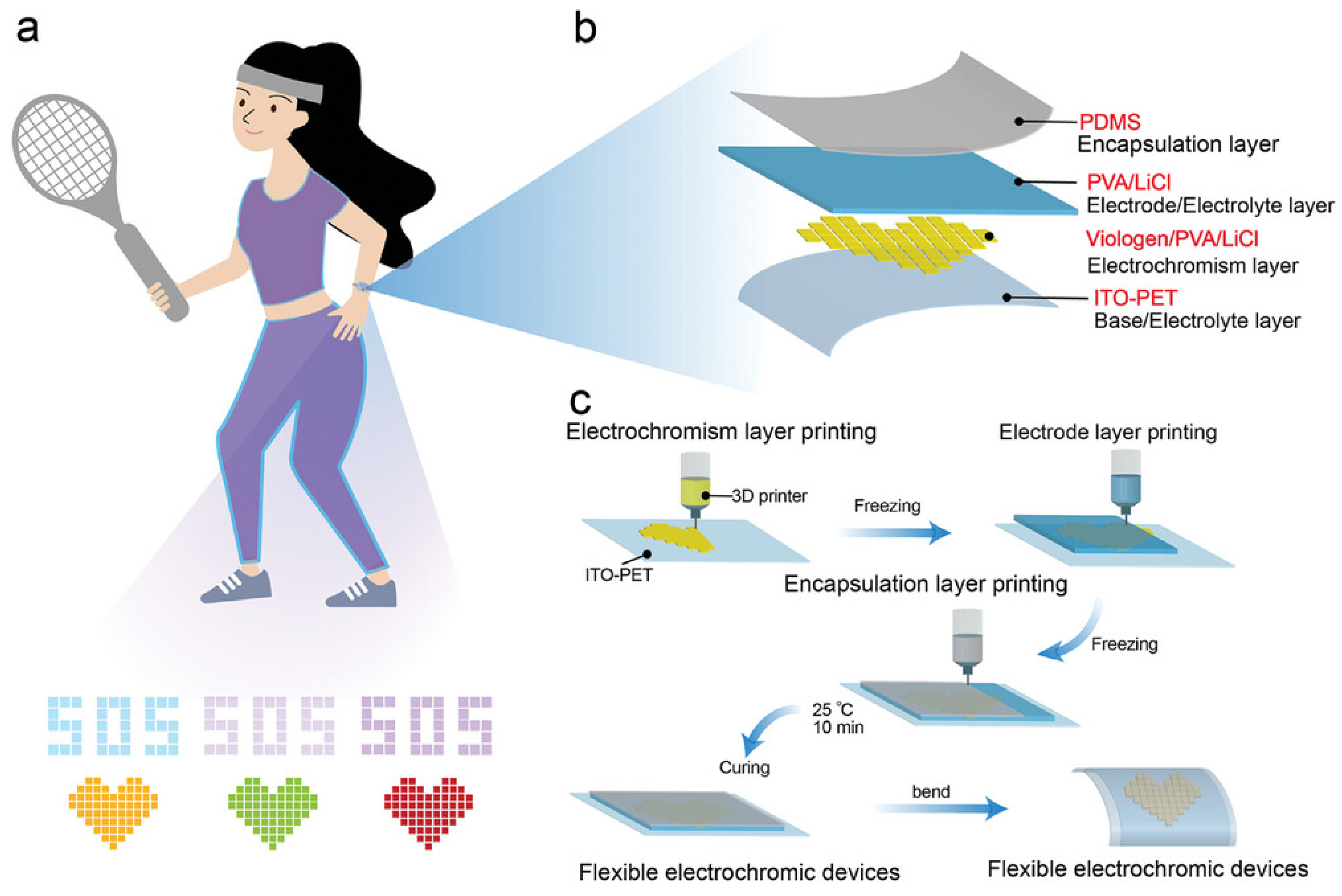
- Luo, X.; Wan, R.; Zhang, Z.; Song, M.; Yan, L.; Xu, J.; Yang, H.; Lu, B. 3D-Printed Hydrogel-Based Flexible Electrochromic Device for Wearable Displays. Adv. Sci. 2024, 11, 2404679. [Google Scholar] [CrossRef] [PubMed]
- Kalkal, A.; Kumar, S.; Kumar, P.; Pradhan, R.; Willander, M.; Packirisamy, G.; Kumar, S.; Malhotra, B.D. Recent Advances in 3D Printing Technologies for Wearable (Bio)Sensors. Addit. Manuf. 2021, 46, 102088. [Google Scholar] [CrossRef]
- Liu, Y.; Zhu, Y. 3D-Printed Soft Wearable Electronics: Techniques, Materials, and Applications. In Additive Manufacturing; Zhou, K., Ed.; Springer International Publishing: Cham, Switzerland, 2023; pp. 1–49. [Google Scholar] [CrossRef]
- Guo, Y.; Chen, S.; Sun, L.; Yang, L.; Zhang, L.; Lou, J.; You, Z. Degradable and Fully Recyclable Dynamic Thermoset Elastomer for 3D-Printed Wearable Electronics. Adv. Funct. Mater. 2021, 31, 2009799. [Google Scholar] [CrossRef]
- Zhang, S.; Wang, S.; Zheng, Y.; Yang, R.; Dong, E.; Lu, L.; Xuan, S.; Gong, X. Coaxial 3D-Printed and Kirigami-Inspired Deployable Wearable Electronics for Complex Body Surfaces. Compos. Sci. Technol. 2021, 216, 109041. [Google Scholar] [CrossRef]
- Yang, H.; Fang, H.; Wang, W.; Zhang, D.; Zhu, J.; Chen, K.; Sun, Y.; Wang, P.; Zhou, Q.; Qi, C.; et al. 3D Printing of Flexible Batteries for Wearable Electronics. J. Power Sources 2024, 602, 234350. [Google Scholar] [CrossRef]
- Tong, Y.; Feng, Z.; Kim, J.; Robertson, J.L.; Jia, X.; Johnson, B.N. 3D Printed Stretchable Triboelectric Nanogenerator Fibers and Devices. Nano Energy 2020, 75, 104973. [Google Scholar] [CrossRef]
- Zhang, P.; Lei, I.M.; Chen, G.; Lin, J.; Chen, X.; Zhang, J.; Cai, C.; Liang, X.; Liu, J. Integrated 3D Printing of Flexible Electroluminescent Devices and Soft Robots. Nat. Commun. 2022, 13, 4775. [Google Scholar] [CrossRef]
- Liu, C.; Huang, N.; Xu, F.; Tong, J.; Chen, Z.; Gui, X.; Fu, Y.; Lao, C. 3D Printing Technologies for Flexible Tactile Sensors toward Wearable Electronics and Electronic Skin. Polymers 2018, 10, 629. [Google Scholar] [CrossRef]
- Goh, G.D.; Yeong, W.Y. Applications of Machine Learning in 3D Printing. Mater. Today Proc. 2022, 70, 95–100. [Google Scholar] [CrossRef]
- Yu, C.; Jiang, J. A Perspective on Using Machine Learning in 3D Bioprinting. Int. J. Bioprinting 2020, 6, 253. [Google Scholar] [CrossRef]
- Stoyanov, S.; Bailey, C. Machine Learning for Additive Manufacturing of Electronics. In Proceedings of the 2017 40th International Spring Seminar on Electronics Technology (ISSE), Sofia, Bulgaria, 10–14 May 2017; pp. 1–6. [Google Scholar] [CrossRef]
- Velazquez, L. A Machine Learning Approach to Robotic Additive Manufacturing of UV-Curable Polymers Using Direct Ink Writing. Master’s Theses, Louisiana State University, Baton Rouge, Louisiana, 2022. [Google Scholar] [CrossRef]
- Brishty, F.P.; Urner, R.; Grau, G. Machine Learning Based Data Driven Inkjet Printed Electronics: Jetting Prediction for Novel Inks. Flex. Print. Electron. 2022, 7, 015009. [Google Scholar] [CrossRef]
- Wu, M.-J.; Chang, M.-C.; Chung, C.-C.; Pancham, P.P.; Yen, T.-J.; Lo, C.-Y. Electromagnetic Characteristic Estimation on Spiral Antennas through AOI, ML, and AI. Flex. Print. Electron. 2022, 7, 025012. [Google Scholar] [CrossRef]
- Zhao, H.; Hefenbrock, M.; Beigl, M.; Tahoori, M.B. Highly-Dependable Printed Neuromorphic Circuits Based on Additive Manufacturing. Flex. Print. Electron. 2023, 8, 025018. [Google Scholar] [CrossRef]
- Tsai, M.-L.; Qiu, R.-Q.; Wu, K.-Y.; Hsu, T.-H.; Li, M.-H.; Lo, C.-Y. Machine-Learning Based Characteristic Estimation Method in Printed Circuit Board Production Lines. Flex. Print. Electron. 2023, 8, 034001. [Google Scholar] [CrossRef]
- Yang, Q.; Vriza, A.; Castro Rubio, C.A.; Chan, H.; Wu, Y.; Xu, J. Artificial Intelligence for Conjugated Polymers. Chem. Mater. 2024, 36, 2602–2622. [Google Scholar] [CrossRef]
- Guo, K.; Yang, Z.; Yu, C.-H.; Buehler, M.J. Artificial Intelligence and Machine Learning in Design of Mechanical Materials. Mater. Horiz. 2021, 8, 1153–1172. [Google Scholar] [CrossRef]
- Plathottam, S.J.; Rzonca, A.; Lakhnori, R.; Iloeje, C.O. A Review of Artificial Intelligence Applications in Manufacturing Operations. J. Adv. Manuf. Process. 2023, 5, e10159. [Google Scholar] [CrossRef]
- Polomoshnov, M.; Reichert, K.-M.; Rettenberger, L.; Ungerer, M.; Hernandez-Sosa, G.; Gengenbach, U.; Reischl, M. Image-Based Identification of Optical Quality and Functional Properties in Inkjet-Printed Electronics Using Machine Learning. J. Intell. Manuf. 2025, 36, 2709–2726. [Google Scholar] [CrossRef]
- Li, M.; Yin, S.; Liu, Z.; Zhang, H. Machine Learning Enables Electrical Resistivity Modeling of Printed Lines in Aerosol Jet 3D Printing. Sci. Rep. 2024, 14, 14614. [Google Scholar] [CrossRef]
- Ivy, L.; Xie, Y.; Lobo, T.; Gund, V.; Davaji, B.; Garud, M.; Doerschuk, P.; Lal, A. Feature-Based Machine Learning for Predicting Resistances in Printed Electronics. In Proceedings of the 2023 IEEE International Conference on Flexible and Printable Sensors and Systems (FLEPS), Boston, MA, USA, 9–12 July 2023; pp. 1–4. [Google Scholar] [CrossRef]
- Lall, P.; Soni, V.; Kulkarni, S.; Miller, S. Comparison of Machine Learning Approaches for Correlating Print Process Parameters to Realized Physical and Electrical Characteristics of Printed Electronics Using Inkjet Platform. In Proceedings of the ASME 2023 International Technical Conference and Exhibition on Packaging and Integration of Electronic and Photonic Microsystems, San Diego, CA, USA, 24–26 October 2023. [Google Scholar] [CrossRef]
- Pillai, A.N.; Subramania, S. A Reliable and Intelligent Ink Selection System for Printed Electronics Using Artificial Neural Network. Int. J. Eng. Trends Technol. 2024, 72, 193–201. [Google Scholar]
- Ghosh, S.; Johnson, M.V.; Neupane, R.; Hardin, J.; Berrigan, J.D.; Kalidindi, S.R.; Kong, Y.L. Machine Learning-Enabled Feature Classification of Evaporation-Driven Multi-Scale 3D Printing. Flex. Print. Electron. 2022, 7, 014011. [Google Scholar] [CrossRef] [PubMed]
- Abbasi Shirsavar, M.; Taghavimehr, M.; Ouedraogo, L.J.; Javaheripi, M.; Hashemi, N.N.; Koushanfar, F.; Montazami, R. Machine Learning-Assisted E-Jet Printing for Manufacturing of Organic Flexible Electronics. Biosens. Bioelectron. 2022, 212, 114418. [Google Scholar] [CrossRef] [PubMed]
- Tom, G.; Schmid, S.P.; Baird, S.G.; Cao, Y.; Darvish, K.; Hao, H.; Lo, S.; Pablo-García, S.; Rajaonson, E.M.; Skreta, M.; et al. Self-Driving Laboratories for Chemistry and Materials Science. Chem. Rev. 2024, 124, 9633–9732. [Google Scholar] [CrossRef] [PubMed]
- Sarkar, N.; Strathearn, D.; Lee, G.; Olfat, M.; Mansour, R.R. A 0.25 mm3 Atomic Force Microscope on-a-Chip. In Proceedings of the 2015 28th IEEE International Conference on Micro Electro Mechanical Systems (MEMS), Estoril, Portugal, 18–22 January 2015; pp. 732–735. [Google Scholar] [CrossRef]
- Siemenn, A.E.; Das, B.; Aissi, E.; Sheng, F.; Elliott, L.; Hudspeth, B.; Meyers, M.; Serdy, J.; Buonassisi, T. Archerfish: A Retrofitted 3D Printer for High-Throughput Combinatorial Experimentation via Continuous Printing. Digit. Discov. 2025, 4, 896–909. [Google Scholar] [CrossRef]
- Deed—Attribution-NonCommercial 3.0 Unported—Creative Commons. Available online: https://creativecommons.org/licenses/by-nc/3.0/ (accessed on 17 May 2025).
- Liu, Q.; Forrester, M.F.; Dileep, D.; Subbiah, A.; Garg, V.; Finley, D.; Cochran, E.W.; Kraus, G.A.; Broderick, S.R. Data-Driven Modeling and Design of Sustainable High Tg Polymers. Int. J. Mol. Sci. 2025, 26, 2743. [Google Scholar] [CrossRef]
- Bao, Y. Recent Trends in Advanced Photoinitiators for Vat Photopolymerization 3D Printing. Macromol. Rapid Commun. 2022, 43, 2200202. [Google Scholar] [CrossRef]
- Ahn, D.; Stevens, L.M.; Zhou, K.; Page, Z.A. Rapid High-Resolution Visible Light 3D Printing. ACS Cent. Sci. 2020, 6, 1555–1563. [Google Scholar] [CrossRef]
- Chekkaramkodi, D.; Jacob, L.; Shebeeb, C.M.; Umer, R.; Butt, H. Review of Vat Photopolymerization 3D Printing of Photonic Devices. Addit. Manuf. 2024, 86, 104189. [Google Scholar] [CrossRef]
- Nath, S.S.; Dineshkumar, R.; Prasad, K.; Gupta, D.; Jangir, P.; Kiruba, S. Computational Approaches to Optimize Polymerization and Curing in Low-Temperature Thermosetting Composites for Enhanced Additive Manufacturing Efficiency. Therm. Sci. Eng. Prog. 2025, 58, 103223. [Google Scholar] [CrossRef]


| Method | Accuracy (mm) | Material Compatibility | Surface Finish | Print Speed | Strength | Limitation | Equipment Cost |
|---|---|---|---|---|---|---|---|
| FDM | ±0.05 –0.3 | Thermoplastic | Moderate | 0.04–0.15 m/s | Low cost, Robust | Layer lines | $200– $15,000 |
| SLA | ±0.025 –0.1 | Photopolymer | Excellent | 10–100 mm/h | High accuracy | Limited materials | $2500– $25,000 |
| DLP | ±0.025 –0.1 | Photopolymer | Excellent | 20–100 mm/h | Faster than SLA | Limited materials | $5000– $50,000 |
| SLS | ±0.05 –0.2 | Thermoplastics & composites | Rough | 10–50 mm3/s | Mechanical properties | Powder hazard | $30,000– $200,000 |
| Poly Jet | ±0.01 –0.085 | Photopolymer | Excellent | 0.1–0.2 m/s | Very High Resolution | Expensive | $50,000– $500,000 |
| DIW | ±0.1 –0.5 | Exceptionally wide | Moderate | 0.001–0.5 m/s | Print multi- materials | Viscosity requirement | $10,000– $100,000 |
| Method | Accuracy (%) | Interpret -Ability | Training Need | Use Cases | Adaptability to New Uses | Computational Cost/Complexity |
|---|---|---|---|---|---|---|
| SVM | 80–85 | High (SHAP) | Low– Moderate | Defect classification, Parameter prediction, Optimization | Moderate | Low to Moderate |
| ANN | 80–97 | Low | High | Mechanical property prediction, thermal modeling | Limited | Moderate to High |
| CNN | 92–98 | Low– Moderate | High | Layer inspection, defect detection from images | Limited | High |
| GAN | 90–99 | Low | Very High | Generation of synthetic data, design | Limited | Very High |
| Random Forest | 80–90 | Moderate (feature importance) | Moderate | Materials Screening | High | Moderate |
| BO | N/A (Optimi- zation) | Moderate (Visualizable) | Low | Multi-parameter tuning | High | Moderate |
| Pareto Front | Optimi- zation | Low | Moderate | Multi-parameter trade-off | Moderate | High |
| Improvements by AI | Materials/Process | Model | Ref |
|---|---|---|---|
| Enhanced interfaces and sensor design | 3D printed particle-matrix composite | Computer vision, finite element analysis | [135] |
| Enhanced reliability | 3D printed neuromorphic circuits | Gradient-based optimization | [158] |
| Jetting prediction for new inks | Inkjet printed electronics | Decision trees, random forest, gradient boosting, and neural networks | [156] |
| Estimating electromagnetic characteristics | Spiral antennas | Gaussian regression | [157] |
| Property estimation | Printed circuit board (PCB) | Computer vision for automatic optical inspection (AOI) | [159] |
| Resistivity modeling of printed lines | 3D aerosol-jet printing | Convolutional neural networks | [164] |
| Predicting resistance | PCB | Computer vision | [165] |
| Relating print parameters to physical and electrical properties | Inkjet-printed electronics | Nonlinear regression, k-nearest neighbor (KNN), Gaussian process regression | [166] |
| Ink selection system | Screen-printed electronics | MLP | [167] |
| Identification of optical quality and functionality | Inkjet-printed electronics | Computer Vision | [163] |
| Feature classification | Evaporation-drivenmulti-scale 3D printing | SVM | [168] |
| Classification of electrical conductivity based on voltage, nozzle speed, and flow rate | Electro-hydrodynamic-jet of organic electronics | Decision tree classifier, KNN, random forest | [169] |
| Strain and humidity sensorsfor health monitoring | Graphene-carbon nanotube ink for jet printing | SVM | [154] |
Disclaimer/Publisher’s Note: The statements, opinions and data contained in all publications are solely those of the individual author(s) and contributor(s) and not of MDPI and/or the editor(s). MDPI and/or the editor(s) disclaim responsibility for any injury to people or property resulting from any ideas, methods, instructions or products referred to in the content. |
© 2025 by the authors. Licensee MDPI, Basel, Switzerland. This article is an open access article distributed under the terms and conditions of the Creative Commons Attribution (CC BY) license (https://creativecommons.org/licenses/by/4.0/).
Share and Cite
Chen, J.; Yuan, Y.; Wang, Q.; Wang, H.; Advincula, R.C. Bridging Additive Manufacturing and Electronics Printing in the Age of AI. Nanomaterials 2025, 15, 843. https://doi.org/10.3390/nano15110843
Chen J, Yuan Y, Wang Q, Wang H, Advincula RC. Bridging Additive Manufacturing and Electronics Printing in the Age of AI. Nanomaterials. 2025; 15(11):843. https://doi.org/10.3390/nano15110843
Chicago/Turabian StyleChen, Jihua, Yue Yuan, Qianshu Wang, Hanyu Wang, and Rigoberto C. Advincula. 2025. "Bridging Additive Manufacturing and Electronics Printing in the Age of AI" Nanomaterials 15, no. 11: 843. https://doi.org/10.3390/nano15110843
APA StyleChen, J., Yuan, Y., Wang, Q., Wang, H., & Advincula, R. C. (2025). Bridging Additive Manufacturing and Electronics Printing in the Age of AI. Nanomaterials, 15(11), 843. https://doi.org/10.3390/nano15110843