Article

Investigation of Annealing Temperature Effect of Tin Oxide on the Efficiency of Planar Structure Perovskite Solar Cells

by
Ahmed Hayali
1,* and
Maan M. Alkaisi
2,3,*
1
Department of Computer Networks and the Internet, College of Information Technology, Ninevah University, Mosul 41001, Iraq
2
Department of Electrical and Computer Engineering, University of Canterbury, Christchurch 8041, New Zealand
3
The MacDiarmid Institute for Advanced Materials and Nanotechnology, Wellington 6140, New Zealand
*
Authors to whom correspondence should be addressed.
Nanomaterials 2025, 15(11), 807; https://doi.org/10.3390/nano15110807 (registering DOI)
Submission received: 16 April 2025 / Revised: 17 May 2025 / Accepted: 20 May 2025 / Published: 28 May 2025
(This article belongs to the Special Issue Low-Dimensional Perovskite Materials and Devices)

Abstract

:
Tin oxide (SnO2) is an attractive candidate for the electron transport layer (ETL) in perovskite-based solar cells because of its low temperature process requirement. The ability to form ETL layers at low temperatures opens up opportunities for the use of flexible and low-cost materials suitable for photovoltaic applications. The ETL is necessary for the extraction of electrons and charge separation from the perovskite active layer. Herein, we present a study of the effect of annealing temperature on SnO2 used as an ETL. The annealing temperature of the SnO2 has a considerable effect on the morphology, crystallinity, grain size, and surface topography of the SnO2 layer. The surface properties of the ETL influence the structural properties of the perovskite films. In this study, the annealing temperature of the SnO2, deposited using spin coating, was changed from 90 °C to 150 °C. The SnO2 films annealed at 120   ° C resulted in reduced surface defects, improved electron extraction, and produced a significant increase in the grain size of the perovskite active layers. The increase in grain size led to improved efficiency of the PSCs. Devices annealed at 120 °C yielded PSCs with an average efficiency of 15% for a 0.36 cm2 active area, while devices treated at 90 °C and 150 °C produced an average efficiency of 12%. The PSCs fabricated at low temperatures provide an effective technique for low-cost manufacturing, especially on flexible and polymer-based substrates.

Graphical Abstract

1. Introduction

PSCs have been explored as a promising new generation of photovoltaic devices due to their outstanding light-harvesting properties, low fabrication cost, and diverse range of applications. Particularly, the power conversion efficiency (PCE) of PSCs has seen sharp increases over the past 15 years. In 2009, the efficiency of the first perovskite device prepared by Kojima et al. was 3.8% using a 0.2 cm2 active area [1]. Then, in just one decade of extensive efforts, the efficiency of PSCs has reached over 26% [2]. Due to the fact that tin oxide (SnO2) possesses good optical and electrical properties, SnO2 has been extensively utilized as an ETL in the fabrication of PSCs. Generally, the SnO2 can be deposited by different methods such as magnetron sputtering [3], chemical vapor deposition (CVD) [4], atomic layer deposition (ALD) [5], the hydrothermal process [6], electrodeposition [7], nebulized spray pyrolysis [8], and the sol-gel process [9]. In this work, the SnO2 ETL was deposited using a low-cost spin coating process.
SnO2 has been studied as a possible alternative material to titanium dioxide (TiO2) for ETLs. This is due to its high electron mobility suitable for electron extraction and similar physical structural properties to TiO2 [10]. Generally, TiO2 has been widely utilized as an ETL for PSCs [11,12,13,14,15]. However, TiO2 has low electron mobility and requires a high annealing temperature up to 500 °C for a duration of one hour [16,17,18]. The high temperature increases the device manufacturing cost and limits the use of flexible substrates. SnO2 has been explored as a substitute for TiO2 and ZnO to reduce manufacturing costs and improve the efficiency of PSC devices [19,20]. Guangfeng et al. have described the fabrication of PSCs using sputtered SnO2 as an ETL and achieved an efficiency of 18.2% using a small active area of 0.14 cm2 [21]. In 2015, Weijun et al. fabricated a perovskite film with CH3NH3PbI3 composition and utilized nanocrystalline SnO2 as an ETL to achieve a PCE of 16% [22]. In the same year, Weijun et al. prepared a vacuum-processed CH3NH3PbI3 perovskite composition and used low-temperature SnO2 as an ETL that achieved an average efficiency of 14% [23]. Qi et al. prepared perovskite using solution-processed SnO2 nanoparticles as an ETL and achieved an efficiency of 19.9% using an active area of 0.108 cm2 [24].
Generally, the photovoltaic devices and their photoelectric properties are significantly influenced by the crystallographic orientation of the perovskite active layer crystal structure [25]. The interfaces between the perovskite active layer and ETL show high defect concentrations that influence the perovskite film morphology. This causes a drop in open circuit voltage. Therefore, the topography and grain size of perovskite films are affected by the surface roughness of ETL, which influences the performance of devices [26].
The mesoscopic perovskite structure conventionally uses TiO2 as the ETL material; however, TiO2 needs to be annealed at a high temperature of 500 °C, which may hinder the large-scale commercialization of perovskite devices. Low temperatures and a simple fabrication method are the two parameters that are essential requirements for researchers and for the photovoltaic industry [27,28,29].
In this study, a low annealing temperature of SnO2 was examined in the range from 90 °C to 150 °C. The triple cation perovskite with n-i-p planar structure and a chemical formula of“CsI0.05[(FAPbI3)0.85 (MAPbBr3)0.15]0.95”was prepared at room temperature, as mentioned elsewhere [11,13]. Generally, the interfaces between the perovskite film and the ETL play a significant role in the performance of the PSCs. We have investigated the influence of changing the annealing temperature on the properties of SnO2 and its impact on the performance of PSCs. Herein, to understand the effect of changing the annealing temperature of SnO2 on the efficiency of PSCs, the optical and electrical properties of SnO2 and the perovskite active layer deposited on the ETL with different annealing temperatures were studied.
Our results suggest that perovskite films grown outside the glovebox and under ambient laboratory conditions (25 °C temperature and 45% humidity) are suitable for flexible substrate applications when combined with a low-temperature SnO2 ETL process.

2. Materials and Methods

2.1. Materials

All materials in this study were used as received from suppliers without any purification. The substrates used were “fluorine-doped tin oxide (FTO) soda lime glass with resistivity (12–15 Ω/sq), purchased from MSE proTM supplies (Tucson, AZ, USA). Methylammonium bromide (MABr) and formamidinium iodide (FAI) were purchased from GreatCell Solar. Lead (II) iodide (PbI2) 99.9% and lead (II) bromide (PbBr2) 99.9% were bought from Luminescence Technology Corp. (Lumtec), Hsin-Chu City, Taiwan. Acetonitrile anhydrous (99.8%) tin(II) chloride dehydrate SnCl2·2H2O, spiro-MeOTAD 99% (HPLC), chlorobenzene (CBZ) (95%), and 4-tert-Butylpyridine (TBP 98%) were procured from Sigma-Aldrich (Saint Louis, MO, USA). Cesium iodide (CsI 99.998%) was acquired from Alfa Aesar (Leicestershire, UK). Dimethyl sulfoxide (DMSO, 99.9%) and N,N-dimethylformamide (DMF, 99.5%) were bought from Fisher Scientific (Waltham, MA, USA).”

2.2. Methods

In this research, the “FTO glass substrate (12–15 Ω/sq)” was etched from one edge using zinc powder and dilute HCL to avoid a short-circuit problem. Then, the FTO glass substrate was washed with deionized water, followed by cleaning with acetone, methanol, and IPA each for 15 min in an ultrasonic bath. The ETL consists of two main layers: a compact TiO2 layer and an SnO2 layer. The compact TiO2 was prepared using a DC-sputtering technique with a titanium target and argon (6 sccm)-to-oxygen (12 sccm) ratio as mentioned elsewhere in more detail [11]. To clean and improve the hydrophilicity of the compact TiO2 surface, oxygen plasma ashing was applied for 10 min before SnO2 deposition. The SnO2 was prepared by dissolving 22.565 mg of SnCl2·2H2O in 1 mL of ethanol. Then, the SnCl2·2H2O precursor solutions were applied on the compact TiO2 by spin coating at 3000 RPM for 40 s. Then, it was heated on a hot plate in a laboratory at 120 °C for 30 min. In this study, the annealing temperature of SnO2 was investigated at three temperatures: 90 °C, 120 °C, and 150 °C.
The triple cation perovskite was prepared by two methods, as explained in more detail elsewhere [11,12,13]. The main material compositions used to prepare the perovskite material were MABr (0.2M), FAI (1M), PbBr2 (0.2M), PbI2 (1.1M), and CsI (1.5M), and then a 10% solution of acetonitrile was added to the perovskite precursor solution. The resulting perovskite composition was applied on the ETL in an ambient air laboratory using two spin coating steps. First, 100 µL of precursor solution was spun onto the SnO2 at 1000 RPM for 15 s. This coated the entire sample. Second, the spinning speed was increased to 6000 RPM for 30 s. Finally, after 20 s waiting time, 200 µL of CBZ was dispensed on the samples before the end of the spinning to dispose of the DMSO/DMF. Then, the perovskite film was annealed on the hot plate at 100 °C for half an hour, as mentioned elsewhere [13]. The hole transport layer (HTL) was prepared by dissolving spiro-MeOTAD (80 mg) in chlorobenzene (1 mL) and adding 29 μL of 4-tert-butylpyridine (TBP), before 18ΜL of Li+ salt TFSI was added. A total of 100 µL of this composition was dispensed on the active layer and spun at 4000 RPM for 20 s. Finally, the gold electrodes of the device were prepared by electron beam evaporation. The architecture of the full perovskite device and layer thicknesses utilized in this study is shown in Figure 1.
The PCE of the perovskite device was measured using a sunlight simulator AM 1.5G ABET Sun3000 (100 mW/cm2), Milford, USA, and a Keithley meter. A Cary 6000i UV spectrometer (Waldbronn, Germany) was utilized to measure the transparency and absorption spectrum of the SnO2 prepared with different annealing temperatures. The grain size and topography of the SnO2 and perovskite film deposited on the SnO2 treated with different temperatures were measured using a Scanning Electron Microscopy tool (Raith-150) (Dortmund, Germany). A Rigaku Smart-Lab X-ray system (Tokyo, Japan) was used to measure the XRD spectra of the perovskite film deposited on the SnO2 film with different annealing temperatures. The morphology and surface roughness of SnO2 with different annealing temperatures were measured using Digital Instruments AFM from Veeco Instruments Inc. (Aschheim/Dornach, Germany). All measurements of PSCs were conducted in the ambient laboratory at 25 °C temperature and 45% humidity.

3. Results

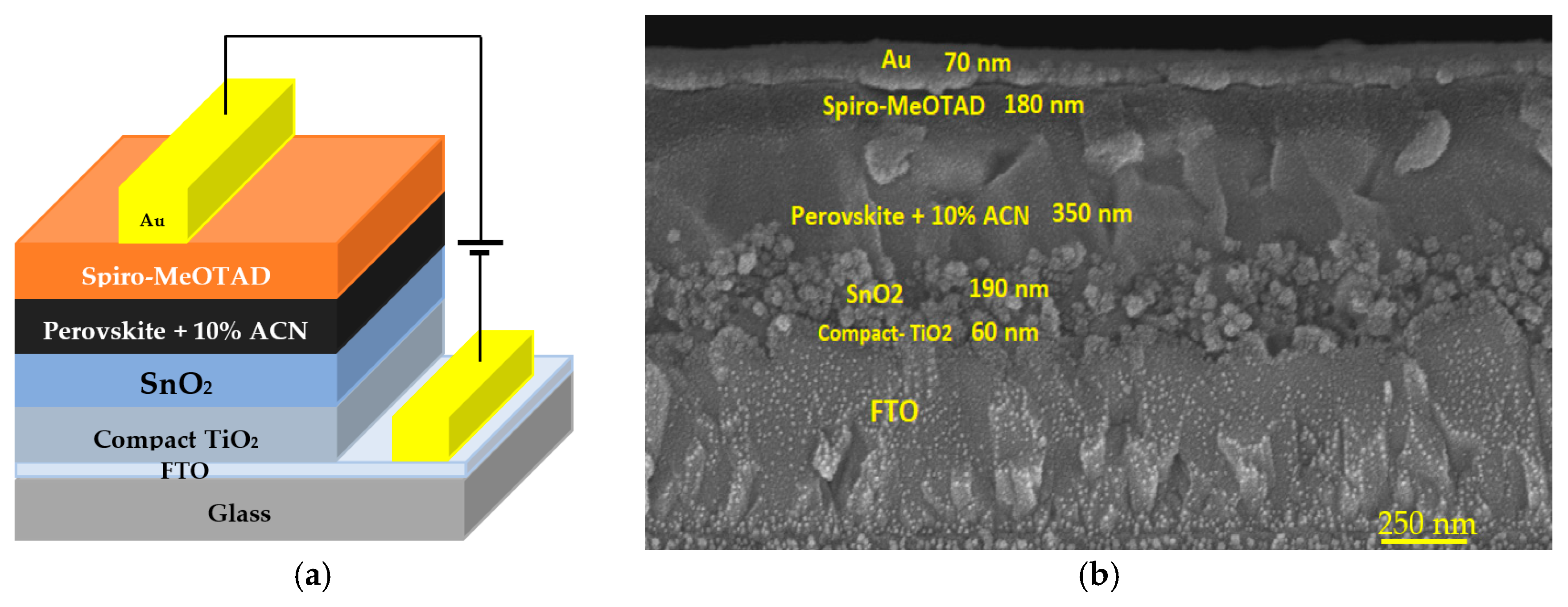
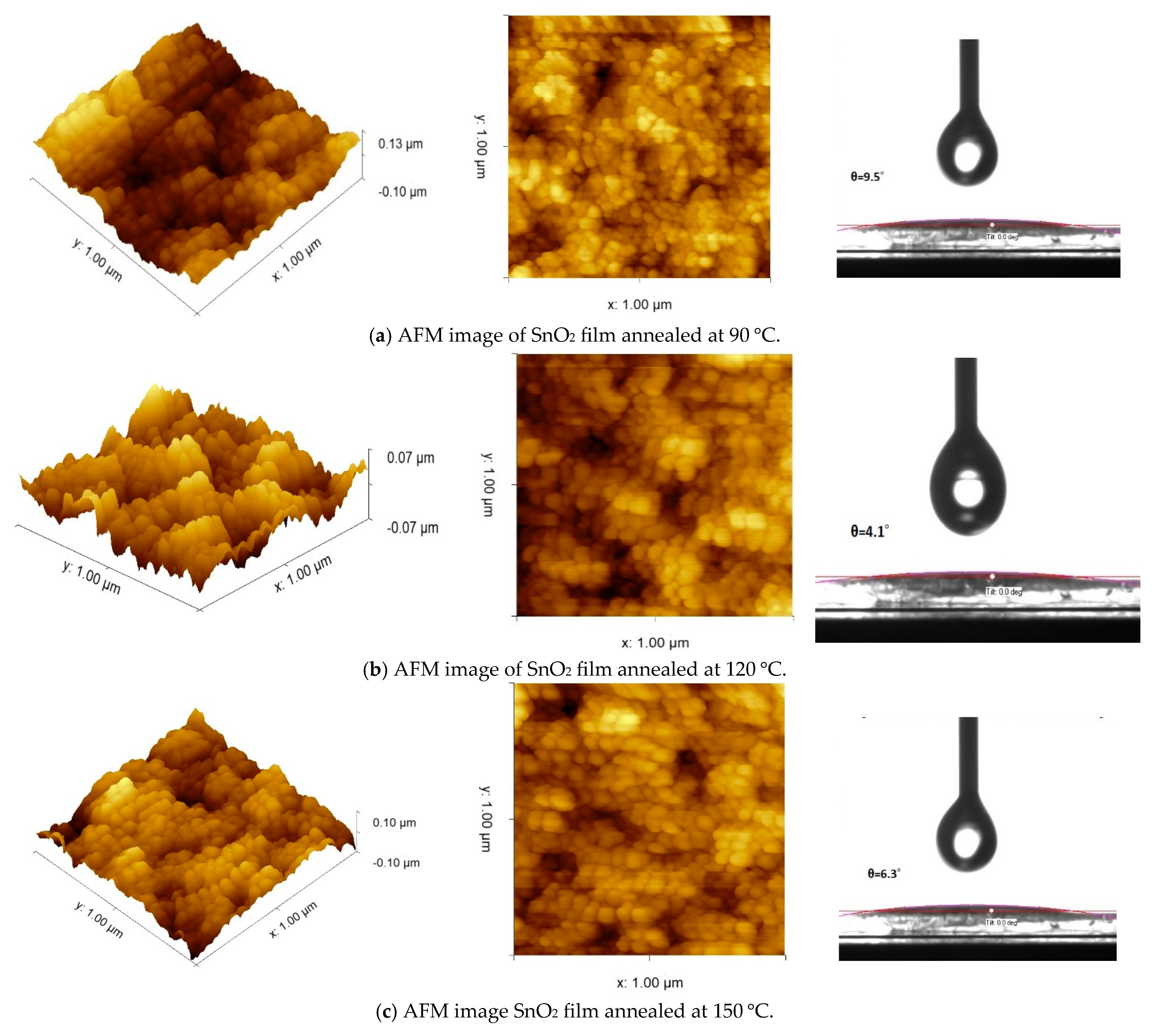
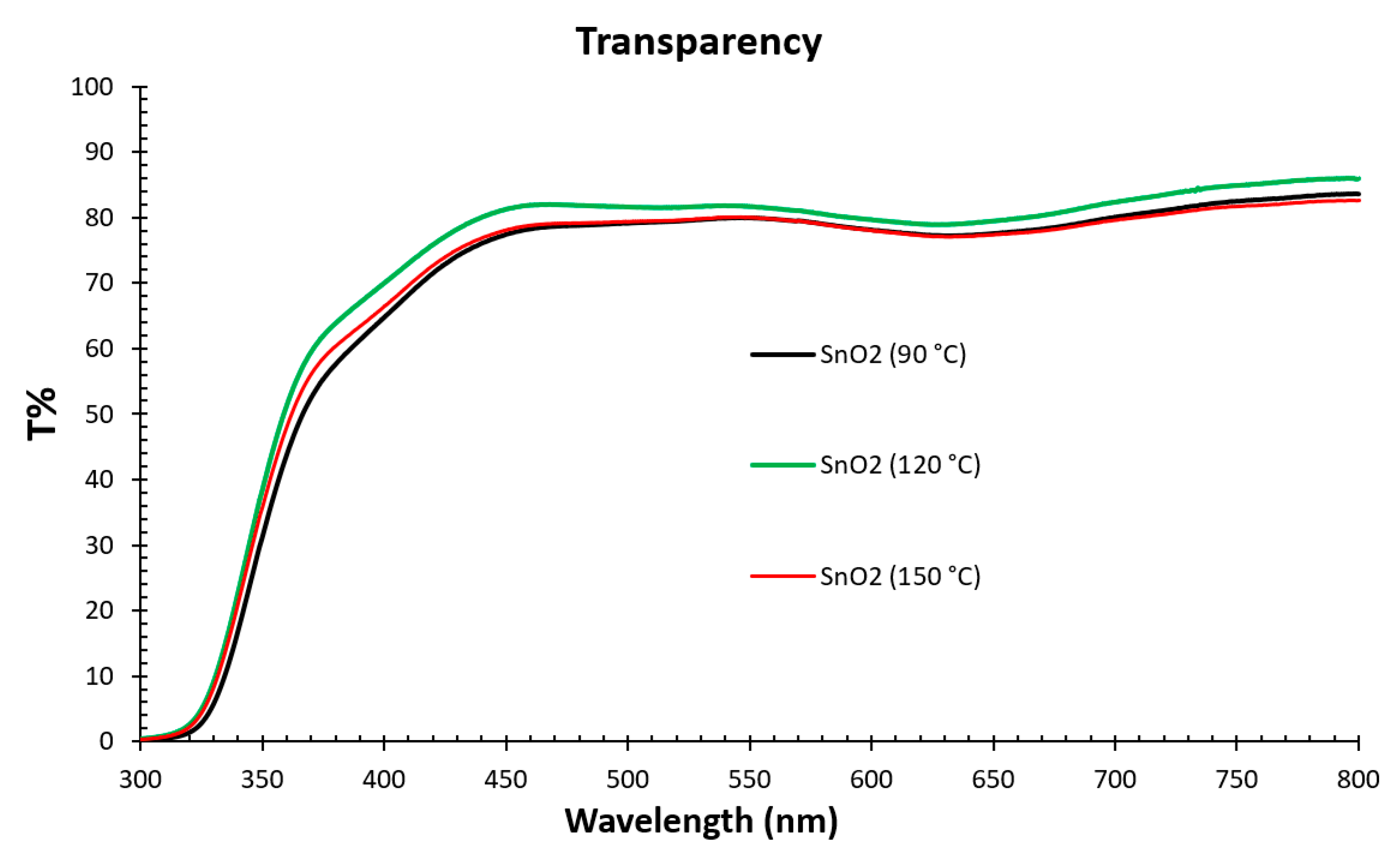
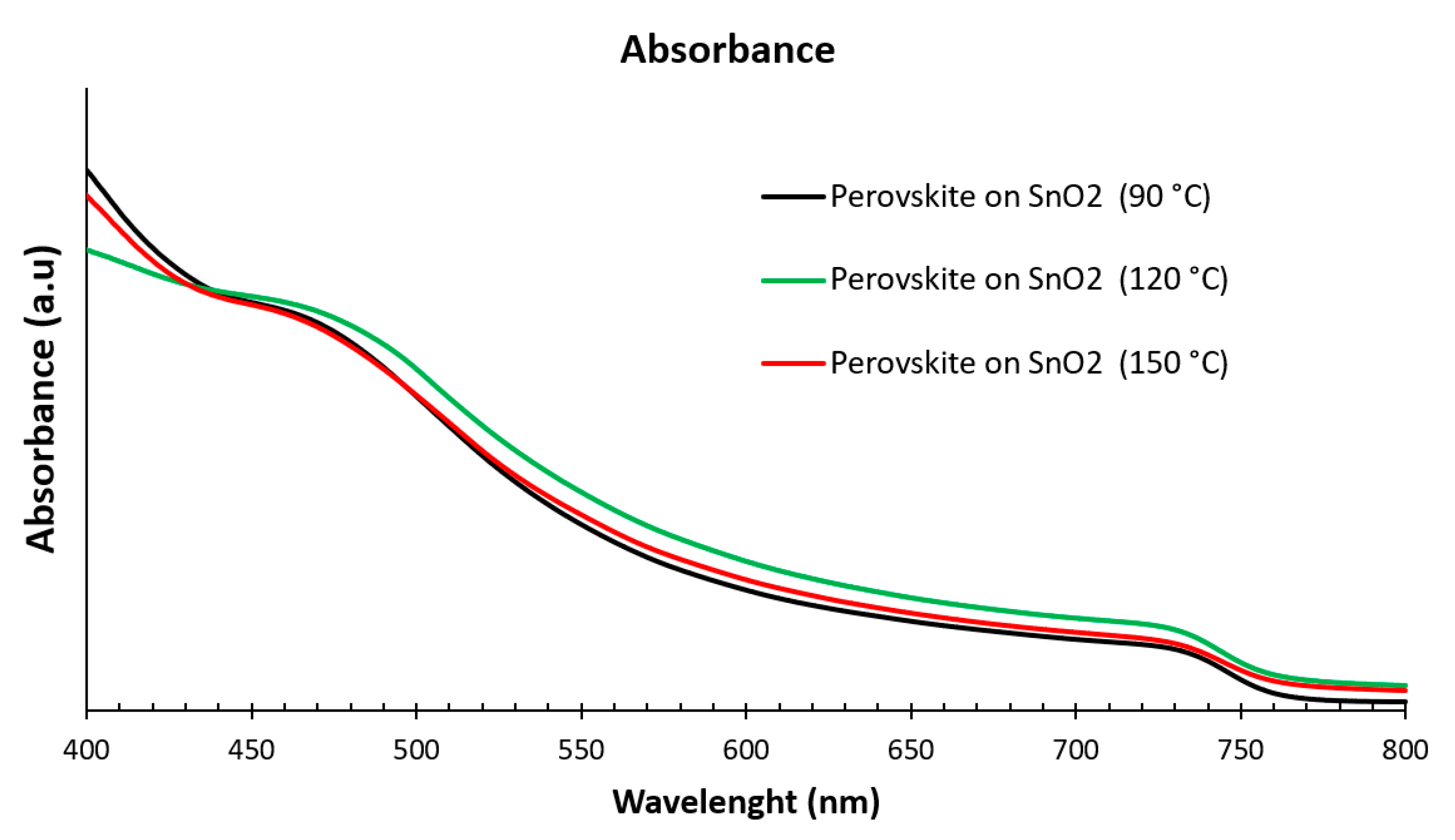
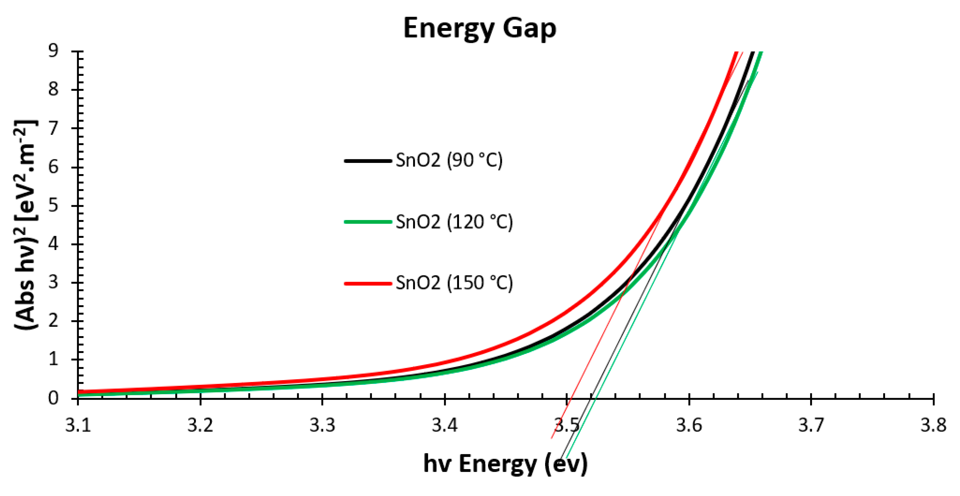
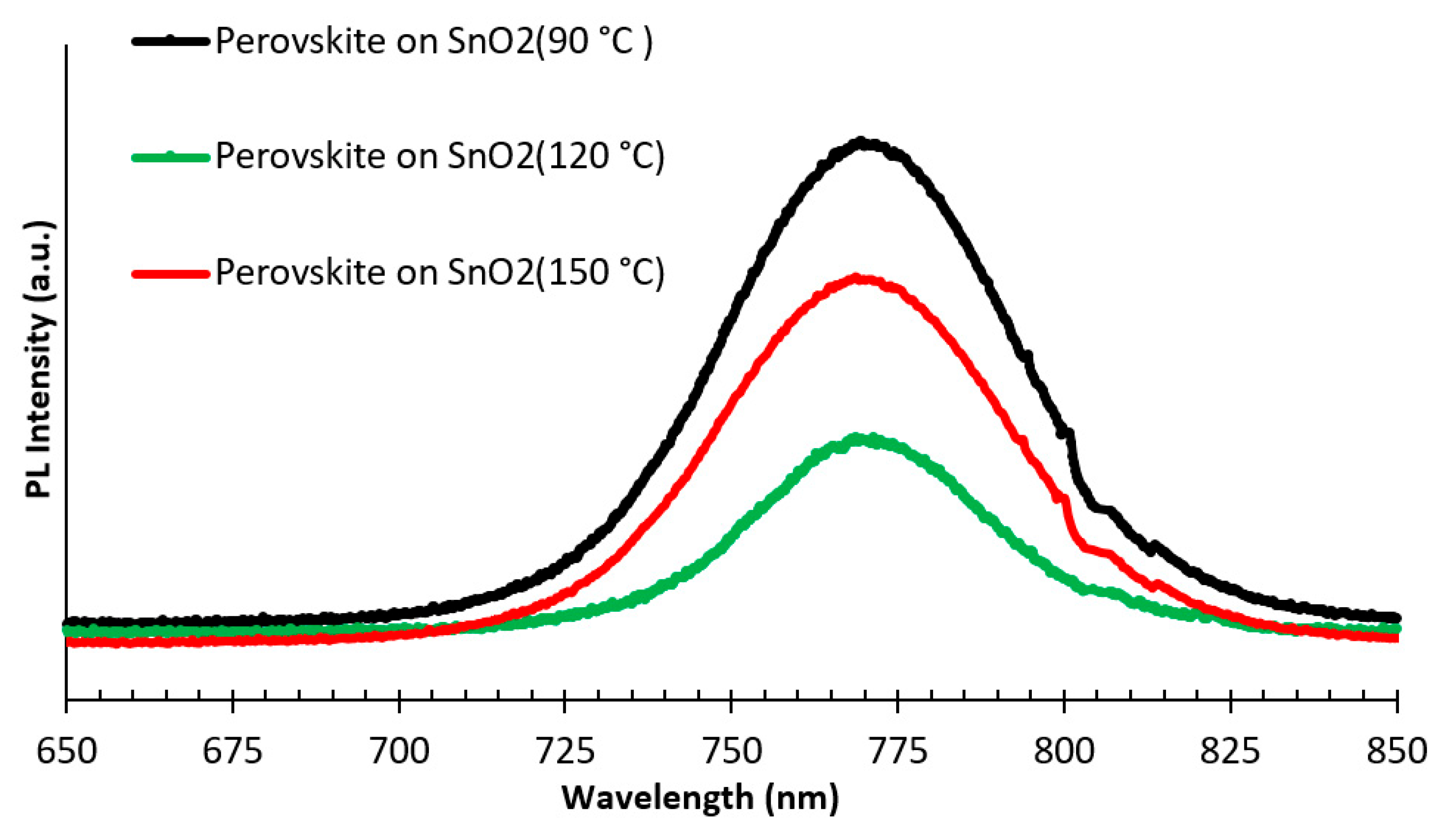
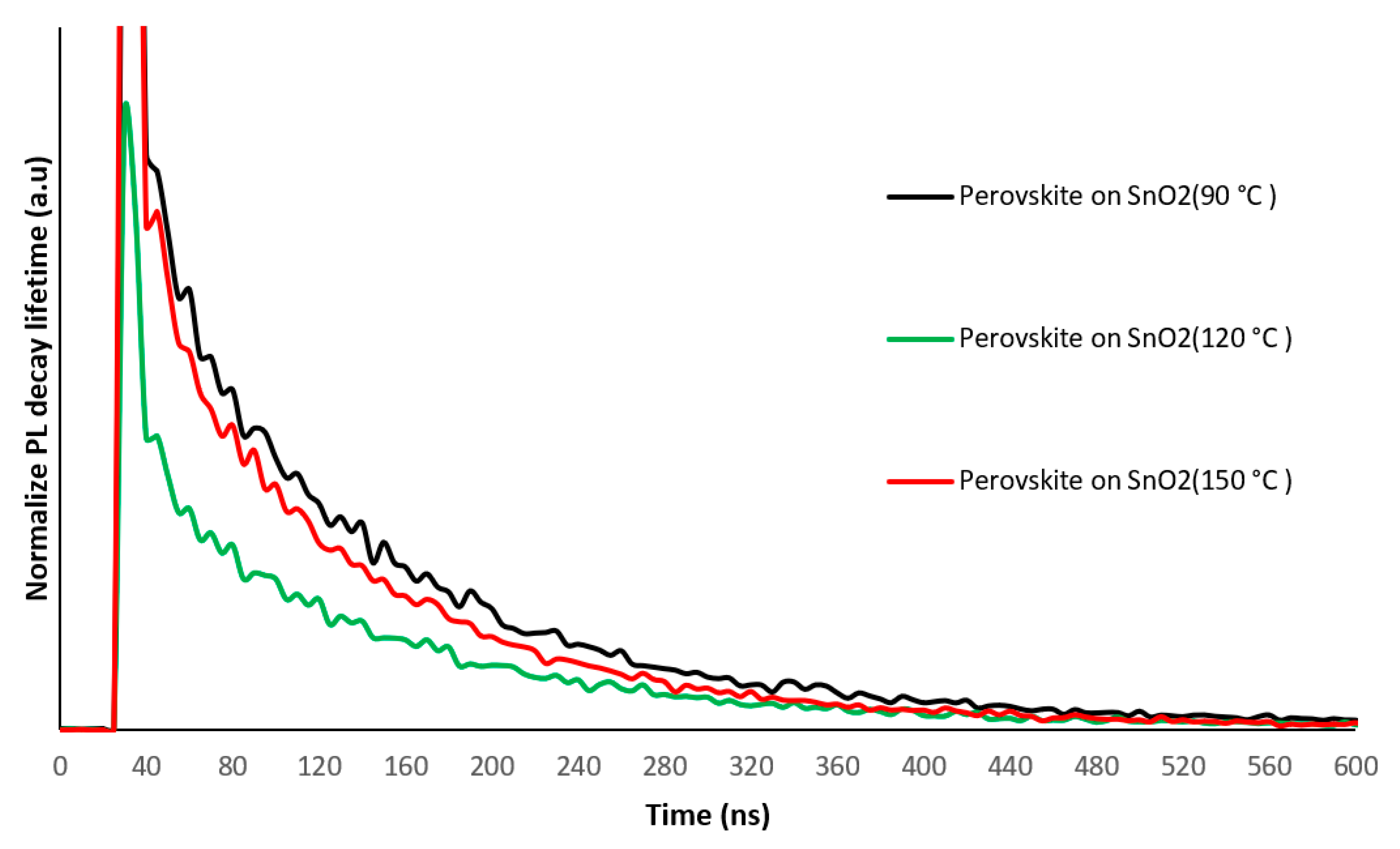
3.1. Structural and Optical Properties of the SnO2 and Perovskite Films

The interface properties between the C-TiO2 and SnO2 are critical for the electron extraction and recombination dynamics. C-TiO2 was deposited on FTO glass, and then SnO2 was deposited on C-TiO2 to decrease backflow of electrons [30]. The perovskite was deposited on the optimized ETL (SnO2/C-TiO2 to enhance the crystallinity of the perovskite active layer during the annealing method and to reduce the hysteresis of the perovskite devices [31]. The annealing temperature of SnO2 was changed from 90 °C to 150 °C. In this study, atomic force microscopy (AFM) was utilized to image the surface morphology of SnO2 annealed at different temperatures. Figure 2 shows the 3D-AFM and 2D-AFM images of SnO2 film annealed at 90 °C, 120 °C and 150 °C. The x–y axes measure from 0 to 1 um and the z-axis ranged from −0.1 µm to 0.13 µm. The root mean square (RMS) surface roughness value of the SnO2 films annealed at 120 °C is 14 nm, while the RMS values of the SnO2 annealed at 90 °C and 150 °C were 23 nm and 20 nm, respectively. This indicates that the SnO2 film annealed at 120 °C exhibits better homogeneity and produces a smoother surface. Moreover, it provides a more uniform surface and a denser grain structure, as shown in Figure 2. These SnO2 surface properties have led to a larger perovskite grain size [32]. The presence of dark and light areas in the AFM image in Figure 2 does not necessarily indicate the presence of cavities in the surface, but rather indicates differences in heights.
A contact angle (θ) measurement was used to measure the “surface wettability (hydrophilicity).” The surface energy properties of phase separation in the perovskite active layer are affected by the uniformity across the ETL materials. Measuring the contact angle θ provides an indication of the surface energy of each layer. The low θ of the ETL demonstrates a good matching between the ETL and the perovskite active layer, which enhances the perovskite film morphology properties [33]. It is shown in Figure 2 that the θ of SnO2 annealed at 120 °C is 4.1°, while the θ values of SnO2 treated at 90 °C and 150 °C are 9.5° and 6.3°, respectively. It is found that SnO2 heated at 120 °C achieved a low contact angle and high hydrophilicity, which can be attributed to the decrease in the surface roughness of the SnO2. Since SnO2 ETL acts as a seed layer for the perovskite deposition, the surface roughness and wettability of SnO2 will affect the topography and grain size of the perovskite active layer [15].
Image J and Origin 9 software (version 1.54p) were used to compute the average grain size and draw a histogram curve. Figure 3 displays the SEM images of the surface morphology of perovskite active layers deposited on SnO2 films annealed at 90 °C, 120 °C, and 150 °C. The following histogram displays the average grain size for each annealing temperature. It is found that the perovskite film deposited on SnO2 annealed at 120 °C showed a uniform structure with an average grain size of 180 nm, which is larger than the grain size of other perovskite films deposited on SnO2 annealed at 90 °C and 150 °C. The average grain sizes of perovskite film deposited on SnO2 annealed at 90 °C and 150 °C are 115 nm and 130 nm, respectively, as shown in the histogram of Figure 3. We found that perovskite films with a large grain size produce a low series resistance (Rs), resulting in improved efficiency of the device [32]. Our results showed that the perovskite active layer deposited on SnO2 annealed at 120   ° C has a larger grain size and fewer defects than other perovskite films deposited on SnO2 annealed at 90 ° C and 150   ° C. Larger grain size leads to enhancement in carrier conduction properties [34].
Figure 4 shows the transparency spectra of the SnO2 film annealed at temperatures of 90 °C, 120 °C, and 150 °C. SnO2 films deposited on the FTO glass substrate annealed at 120 °C have an average transmittancy of 85% in the visible region and a slight antireflection effect at some wavelength range [21]. The high transparency reduces the optical losses and increases the absorption of light in the perovskite film. The SnO2 annealed at 120   ° C has around 5% higher transparency for wavelengths between 350 nm and 800 nm compared to other SnO2 films annealed at 90   ° C and 150 ° C.
Figure 5 illustrates the optical absorption of perovskite film deposited on SnO2 film annealed at 90   ° C, 120   ° C, and 150   ° C. It is clear that the perovskite active layer deposited on SnO2 annealed at 120 °C has a higher absorption coefficient than other perovskite films in the wavelength range of 450–775 nm. There is around a 10% improvement in the performance of the perovskite films deposited on SnO2 annealed at 120 °C compared with the perovskite active layer deposited on SnO2 annealed at 90   ° C and 150   ° C. The perovskite active layer used in this study, when deposited on SnO2 annealed at 120   ° C, performed better when tested for light-harvesting devices. This improvement is due to larger grain size, which leads to an increase in the current density and decreased recombination rates when the device is subjected to light tests [27].
Figure 6 displays the absorbance edge of the SnO2 annealed with different temperatures. This figure also shows (Abs hυ)2 against hυ (in eV) found from the transmission spectra [35]. The Eg bandgap of SnO2 annealed at 120 °C or 90 °C obtained from the Tauc plot was 3.52 eV, while the Eg was 3.5 eV for SnO2 annealed at 150 °C. A wider Eg offers better hole-blocking ability and can reduce high-energy photon losses, resulting in lower photogenerated carrier losses [36].
To study the defect and charge extraction characteristics of perovskite deposited on SnO2 annealed at different temperatures, photoluminescence (PL) measurements of these different perovskite films deposited on SnO2 were analyzed. Perovskite films deposited on SnO2 annealed at 120 °C showed quenching of the perovskite emission peak at 770 nm. Figure 7 displays the PL spectra of perovskite active layers deposited on SnO2 annealed at 90 °C, 120 °C, and 150   ° C. From the PL spectra of perovskite deposited on SnO2 annealed at 90   ° C, it can be observed that a much stronger PL intensity peak results from high recombination rates in these films. When applying the perovskite active layer on an SnO2 film annealed at 120 °C, the PL spectra peak exhibits notable quenching, indicating effective electron extraction of the ETL and a fast charge transfer. This might be attributed to a comparatively low oxygen vacancy defect density present in the ETL prepared under these conditions [21].
Figure 8 shows the PL decay lifetime of perovskite deposited on SnO2 annealed at different temperatures. It can be seen that the PL decay lifetime of perovskite deposited on SnO2 annealed at 120 °C was 160 ns, while the lifetimes of perovskite deposited on SnO2 annealed at 90   ° C or 150   ° C were 112 ns and 125.5 ns, respectively. The longer carrier lifetime promotes the extraction and transfer of electrons from the perovskite active layer to the ETL before recombination occurs. This is consistent with the PL results [37].
Figure 9 illustrates the external quantum efficiency (EQE) spectra of perovskite deposited on SnO2 annealed at 90 °C, 120 °C, and 150 °C. It is found that perovskite deposited on SnO2 annealed at 120 °C has larger EQE values at the wavelength range between 300 nm and 800 nm, leading to a higher current density when the device is tested under sunlight conditions. The EQE graphs for perovskite deposited on SnO2 annealed at different temperatures exhibited a continued photocurrent generation at wavelengths between 300 and 800 nm and fall outside this wavelength range. The EQE data followed the PL response measurements, indicating that a low PL peak offers larger EQE values [21].
XRD measurements were performed to investigate the effect of changing annealing temperatures of the SnO2 films on the surface quality, crystallinity, and phase structure of the perovskite active layer. It can be seen from Figure 10 that the XRD intensity of the (001) plane of the perovskite deposited on SnO2 annealed at 120 °C is higher than the perovskite deposited on SnO2 annealed at 90 °C and 150 °C. This indicates improved crystallinity of the perovskite active layer with a “high absorption in the short wavelength region” [31]. These results are consistent with the PL spectra results. Our results exhibited a decrease in the PbI2 peak intensity for perovskite devices deposited on SnO2 annealed at 120 °C compared to other devices deposited on SnO2 annealed at 90 °C and 150 °C. This led to a decrease in the hysteresis phenomenon when devices are subjected to current–voltage measurement under sunlight and improved the efficiency of the PSC devices [38].

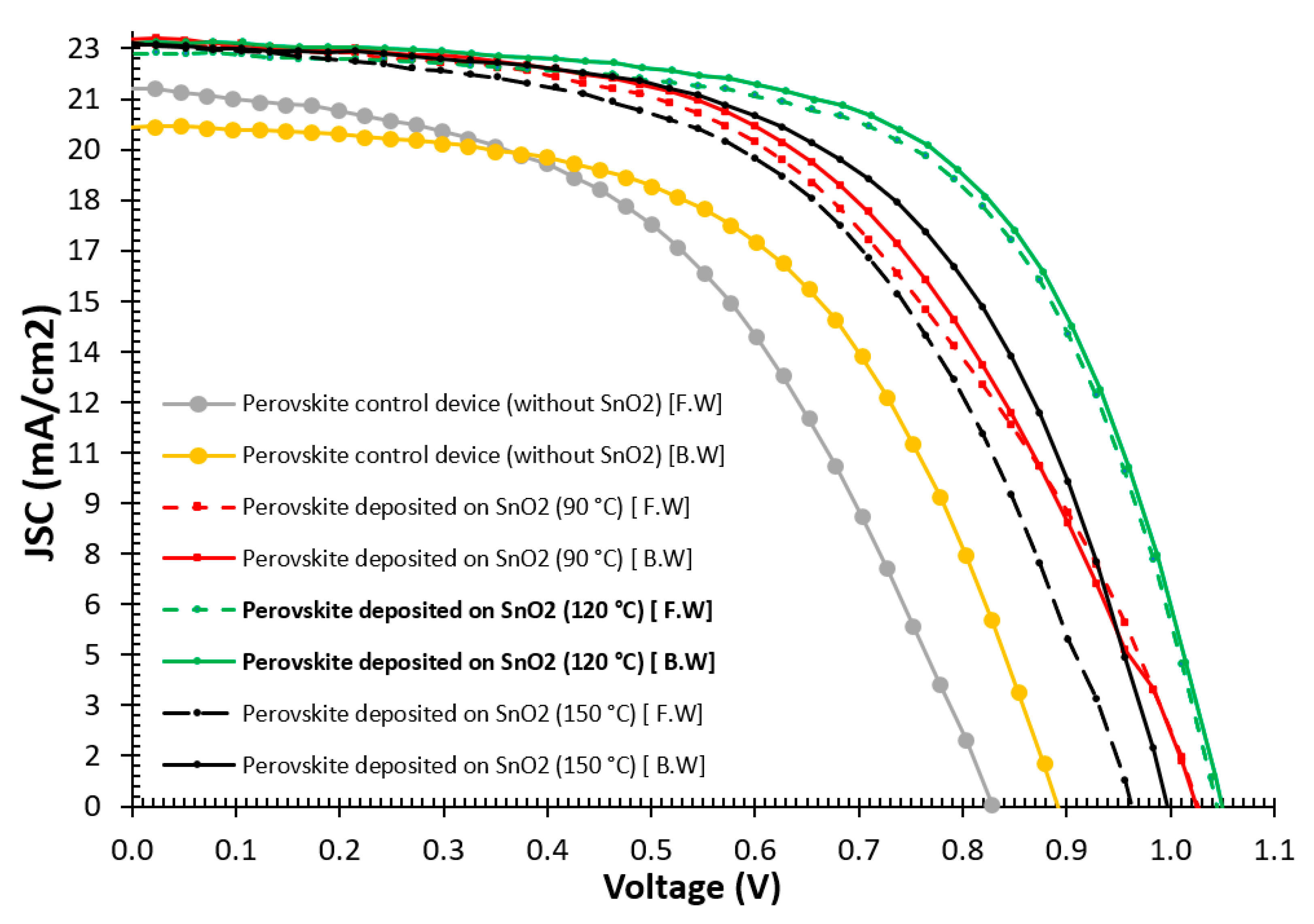
3.2. J-V Characteristics of Perovskite Solar Cells

The annealing temperature of SnO2 was changed from 90   ° C to 150   ° C to achieve the optimum annealing temperature that produced the best device efficiency. Device reproducibility is important for PSC performance with the aim of achieving the highest PCE [39]. Ten samples were fabricated using SnO2 in each experimental run to ensure reproducibility. Table 1 shows key parameters of the perovskite devices (average of 10 samples) deposited on SnO2 at different annealing temperatures. It is demonstrated from the J-V characteristic curves in Figure 11 that perovskite devices deposited on SnO2 annealed at 120 °C yielded the highest average efficiency of 15% based on an active area of 0.36 cm2. The device efficiency improvements are due to the increased perovskite grain size and the decreased recombination rates in the active perovskite layer. The hysteresis index (H.I) was calculated using Formula (1). The hysteresis phenomenon is caused by “charge accumulation, ion migration, trap-assisted charge recombination, and charge redistribution when the voltage is swept forward and backward [40,41,42]. The average PCE of the control sample without SnO2 was 9.4% with an H.I of 14.9%. The drop in efficiency of the control sample is attributed to decreased charge extraction, increased Rs, and charge recombination [7]. The H.I for perovskite devices deposited on SnO2 annealed at 120 °C was less than that used at other annealing temperatures. The perovskite deposited on SnO2 annealed at 120 °C produced around 16% higher efficiency than the PSCs deposited on SnO2 annealed at 90 °C or 150 °C. It is indicated from Table 1 that the open circuit voltage (Voc) of the perovskite deposited on SnO2 annealed at 120 °C is 1034 mV, while the average open circuit voltages of other perovskite devices deposited on SnO2 annealed at 90 °C and 150 °C were 1026 mV and 982 mV, respectively. The fill factor (FF) of the perovskite deposited on SnO2 annealed at 120 °C was 60.8%, while the average FFs of other perovskite devices deposited on SnO2 annealed at 90 °C and 150 °C were 51.8% and 55%, respectively. These improvements of perovskite devices deposited on SnO2 annealed at 120 °C are attributed to the decrease in the Rs from 11.25 to 7.7 Ω·cm2. This was also the reason for the increased current density of 22.65 mA/cm2.
Generally, perovskite devices fabricated at the ambient laboratory conditions of 25 °C temperature and 45% humidity using SnO2 as an ETL, annealed at 120 °C, showed higher PCE and lower hysteresis than other devices using SnO2 annealed at 90 °C or 150 °C. These devices also compared well with devices prepared using TiO2 ETLs in place of SnO2 [14].
Hysteresis index (H.I)% = (EFF%(B.W) − EFF%(F.W))/(EFF%(B.W))

4. Conclusions

Tin oxide (SnO2) was systematically annealed at various temperatures and explored as an ETL. Our results showed that changing the annealing temperature from 90 °C to 150 °C can affect the power conversion efficiency of the PSCs. The average PCE for 10 samples using SnO2 annealed at 120 °C as an ETL was 15% with a 1.3% hysteresis index. The PCE of PSCs fabricated under ambient laboratory conditions with SnO2 annealed at 120 °C increased from 12% to 15% based on a 0.36 cm2 active device area. It should be noted that an active area of 0.36 cm2 is larger than most reported in the literature. The average PCE of the control sample without SnO2 was 9.4% with H.I of 14.9%. The electrical, optical, and morphological properties of SnO2 layers annealed at various temperatures were investigated and correlated to the PSC device performance in terms of efficiency. The perovskite layer deposited on SnO2 annealed at 120 °C has shown an increase in grain size to 180nm and a reduction in the Rs from 11.25 Ω·cm2 to 7.7 Ω·cm2. There is around 10% enhancement in the absorption coefficient of the perovskite film deposited on SnO2 annealed at 120 °C compared to the annealed temperatures of 90 °C and 150 °C. The reduction in Rs has also improved the FF of the perovskite devices to 60.8%. It was found that the PSCs deposited on SnO2 annealed at 120 °C achieved the highest efficiency due to their 85% transparency, minimal surface roughness RMS of 14 nm, low contact angle of 4.1°, PL decay lifetime of 160 ns, and “lower PL intensity, indicating faster charge extraction before recombination occurs”. This study demonstrates the feasibility of low-temperature-processed perovskite devices, paving the way towards low-cost fabrication techniques that are compatible with flexible substrates.

Author Contributions

A.H. conceived the original idea, performed the experimental work, and wrote a manuscript draft. M.M.A. performed analysis, supervised the work, revised the manuscript, and contributed to the discussion of the results. All authors have read and agreed to the published version of the manuscript.

Funding

A.H acknowledges the University of Canterbury, New Zealand. M.M.A. acknowledges the support of the MacDiarmid Institute for Advanced Materials and Nanotechnology, New Zealand. MI funding number: 432D1MMA:E6360:1.

Data Availability Statement

The original contributions presented in the study are included in the article, further inquiries can be directed to the corresponding author.

Acknowledgments

The authors would like to thank Roger Reeves, Physics Department for the optical characterization and Linda Chen, and Gary Turner, from the Nanofabrication Laboratory, University of Canterbury, New Zealand, for providing technical assistance.

Conflicts of Interest

The authors declare no conflicts of interest.

References

  1. Kojima, A.; Teshima, K.; Shirai, Y.; Miyasaka, T. Organometal Halide Perovskites as Visible-Light Sensitizers for Photovoltaic Cells. J. Am. Chem. Soc. 2009, 131, 6050–6051. [Google Scholar] [CrossRef] [PubMed]
  2. Zheng, Y.; Li, Y.; Zhuang, R.; Wu, X.; Tian, C.; Sun, A.; Chen, C.; Guo, Y.; Hua, Y.; Meng, K.; et al. Towards 26% Efficiency in Inverted Perovskite Solar Cells via Interfacial Flipped Band Bending and Suppressed Deep-Level Traps. Energy Environ. Sci. 2023, 17, 1153–1162. [Google Scholar] [CrossRef]
  3. Leng, D.; Wu, L.; Jiang, H.; Zhao, Y.; Zhang, J.; Li, W.; Feng, L. Preparation and Properties of SnO2 Film Deposited by Magnetron Sputtering. Int. J. Photoenergy 2012, 2012, 235971. [Google Scholar] [CrossRef]
  4. Noh, M.F.M.; Arzaee, N.A.; Safaei, J.; Mohamed, N.A.; Kim, H.P.; Yusoff, A.R.M.; Jang, J.; Teridi, M.A.M. Eliminating oxygen vacancies in SnO2 films via aerosol-assisted chemical vapour deposition for perovskite solar cells and photoelectrochemical cells. J. Alloys Compd. 2019, 773, 997–1008. [Google Scholar] [CrossRef]
  5. Lee, Y.; Lee, S.; Seo, G.; Paek, S.; Cho, K.T.; Huckaba, A.J.; Calizzi, M.; Choi, D.w.; Park, J.S.; Lee, D.; et al. Efficient Planar Perovskite Solar Cells Using Passivated Tin Oxide as an Electron Transport Layer. Adv. Sci. 2018, 5, 1800130. [Google Scholar] [CrossRef]
  6. Wu, W.Q.; Chen, D.; Cheng, Y.B.; Caruso, R.A. Thin Films of Tin Oxide Nanosheets Used as the Electron Transporting Layer for Improved Performance and Ambient Stability of Perovskite Photovoltaics. Sol. RRL 2017, 1, 1700117. [Google Scholar] [CrossRef]
  7. Ko, Y.; Kim, Y.R.; Jang, H.; Lee, C.; Kang, M.G.; Jun, Y. Electrodeposition of SnO2 on FTO and Its Application in Planar Heterojunction Perovskite Solar Cells as an Electron Transport Layer. Nanoscale Res. Lett. 2017, 12, 10–16. [Google Scholar] [CrossRef]
  8. Kiruthiga, G.; Rajni, K.S.; Geethanjali, N.; Raguram, T.; Nandhakumar, E.; Senthilkumar, N. SnO2: Investigation of Optical, Structural, and Electrical Properties of Transparent Conductive Oxide Thin Films Prepared by Nebulized Spray Pyrolysis for Photovoltaic Applications. Inorg. Chem. Commun. 2022, 145, 109968. [Google Scholar] [CrossRef]
  9. Karmaoui, M.; Jorge, A.B.; McMillan, P.F.; Aliev, A.E.; Pullar, R.C.; Labrincha, J.A.; Tobaldi, D.M. One-Step Synthesis, Structure, and Band Gap Properties of SnO2 Nanoparticles Made by a Low Temperature Nonaqueous Sol-Gel Technique. ACS Omega 2018, 3, 13227–13238. [Google Scholar] [CrossRef]
  10. Chen, Y.; Meng, Q.; Zhang, L.; Han, C.; Gao, H.; Zhang, Y.; Yan, H. SnO2-Based Electron Transporting Layer Materials for Perovskite Solar Cells: A Review of Recent Progress. J. Energy Chem. 2019, 35, 144–167. [Google Scholar] [CrossRef]
  11. Hayali, A.; Alkaisi, M.M. High Efficiency Perovskite Solar Cells Using DC Sputtered Compact TiO2 electron Transport Layer. EPJ Photovolt. 2021, 12, 8. [Google Scholar] [CrossRef]
  12. Hayali, A.; Reeves, R.J.; Alkaisi, M.M. Wavelength Selective Solar Cells Using Triple Cation Perovskite. Nanomaterials 2022, 12, 3299. [Google Scholar] [CrossRef] [PubMed]
  13. Hayali, A.; Alkaisi, M.M. Improving Charge Transport in Perovskite Solar Cells Using Solvent Additive Technique. Inorganics 2024, 12, 214. [Google Scholar] [CrossRef]
  14. Hayali, A.; Reeves, R.J.; Alkaisi, M.M. Influence of FK209 Cobalt Doped Electron Transport Layer in Cesium Based Perovskite Solar Cells. Appl. Sci. 2022, 12, 9382. [Google Scholar] [CrossRef]
  15. Sidhik, S.; Cerdan Pasarán, A.; Esparza, D.; López Luke, T.; Carriles, R.; De La Rosa, E. Improving the Optoelectronic Properties of Mesoporous TiO2 by Cobalt Doping for High-Performance Hysteresis-Free Perovskite Solar Cells. ACS Appl. Mater. Interfaces 2018, 10, 3571–3580. [Google Scholar] [CrossRef]
  16. Yang, G.; Tao, H.; Qin, P.; Ke, W.; Fang, G. Recent Progress in Electron Transport Layers for Efficient Perovskite Solar Cells. J. Mater. Chem. A 2016, 4, 3970–3990. [Google Scholar] [CrossRef]
  17. Zheng, X.; Wei, Z.; Chen, H.; Zhang, Q.; He, H.; Xiao, S.; Fan, Z.; Wong, K.S.; Yang, S. Designing Nanobowl Arrays of Mesoporous TiO2 as an Alternative Electron Transporting Layer for Carbon Cathode-Based Perovskite Solar Cells. Nanoscale 2016, 8, 6393–6402. [Google Scholar] [CrossRef]
  18. Singh, T.; Öz, S.; Sasinska, A.; Frohnhoven, R.; Mathur, S.; Miyasaka, T. Sulfate-Assisted Interfacial Engineering for High Yield and Efficiency of Triple Cation Perovskite Solar Cells with Alkali-Doped TiO2 Electron-Transporting Layers. Adv. Funct. Mater. 2018, 28, 1706287. [Google Scholar] [CrossRef]
  19. Jiang, Q.; Zhang, X.; You, J. SnO2: A Wonderful Electron Transport Layer for Perovskite Solar Cells. Small 2018, 14, 1801154. [Google Scholar] [CrossRef]
  20. Xiong, L.; Guo, Y.; Wen, J.; Liu, H.; Yang, G.; Qin, P.; Fang, G. Review on the Application of SnO2 in Perovskite Solar Cells. Adv. Funct. Mater. 2018, 28, 1802757. [Google Scholar] [CrossRef]
  21. Bai, G.; Wu, Z.; Li, J.; Bu, T.; Li, W.; Li, W.; Huang, F.; Zhang, Q.; Cheng, Y.B.; Zhong, J. High Performance Perovskite Sub-Module with Sputtered SnO2 Electron Transport Layer. Sol. Energy 2019, 183, 306–314. [Google Scholar] [CrossRef]
  22. Ke, W.; Fang, G.; Liu, Q.; Xiong, L.; Qin, P.; Tao, H.; Wang, J.; Lei, H.; Li, B.; Wan, J.; et al. Lowerature Solution-Processed Tin Oxide as an Alternative Electron Transporting Layer for Efficient Perovskite Solar Cells. J. Am. Chem. Soc. 2015, 137, 6730–6733. [Google Scholar] [CrossRef] [PubMed]
  23. Ke, W.; Zhao, D.; Cimaroli, A.J.; Grice, C.R.; Qin, P.; Liu, Q.; Xiong, L.; Yan, Y.; Fang, G. Effects of Annealing Temperature of Tin Oxide Electron Selective Layers on the Performance of Perovskite Solar Cells. J. Mater. Chem. A 2015, 3, 24163–24168. [Google Scholar] [CrossRef]
  24. Jiang, Q.; Zhang, L.; Wang, H.; Yang, X.; Meng, J.; Liu, H.; Yin, Z.; Wu, J.; Zhang, X.; You, J. Enhanced Electron Extraction Using SnO2 for High-Efficiency Planar-Structure HC(NH2)2PbI3-Based Perovskite Solar Cells. Nat. Energy 2017, 2, 16177. [Google Scholar] [CrossRef]
  25. Jia, S.; Wang, Y.; Liu, H.; Yang, X.; Chen, W. Realization of p-type MA-based perovskite solar cells based on exposure of the (002) facet. Appl. Phys. Lett. 2025, 126, 021104. [Google Scholar] [CrossRef]
  26. Gao, C.; Jia, S.; Yin, X.; Li, Z.; Yang, G.; Chen, J.; Li, Z.; An, X.-T. Enhancing open-circuit voltage in FAPbI3 perovskite solar cells via self-formation of coherent buried interface FAPbIxCl3−x. Chem. Commun. 2025, 61, 2758–2761. [Google Scholar] [CrossRef]
  27. Bu, T.; Liu, X.; Zhou, Y.; Yi, J.; Huang, X.; Luo, L.; Xiao, J.; Ku, Z.; Peng, Y.; Huang, F.; et al. A Novel Quadruple-Cation Absorber for Universal Hysteresis Elimination for High Efficiency and Stable Perovskite Solar Cells. Energy Environ. Sci. 2017, 10, 2509–2515. [Google Scholar] [CrossRef]
  28. Eperon, G.E.; Burlakov, V.M.; Docampo, P.; Goriely, A.; Snaith, H.J. Morphological Control for High Performance, Solution-Processed Planar Heterojunction Perovskite Solar Cells. Adv. Funct. Mater. 2014, 24, 151–157. [Google Scholar] [CrossRef]
  29. Yang, D.; Zhou, X.; Yang, R.; Yang, Z.; Yu, W.; Wang, X.; Li, C.; Liu, S.; Chang, R.P.H. Surface Optimization to Eliminate Hysteresis for Record Efficiency Planar Perovskite Solar Cells. Energy Environ. Sci. 2016, 9, 3071–3078. [Google Scholar] [CrossRef]
  30. Yang, H.; Li, P.; Zhang, J.; Lin, Y. TiO2 Compact Layer for Dye-Sensitized SnO2 Nanocrystalline Thin Film. Electrochim. Acta 2014, 147, 366–370. [Google Scholar] [CrossRef]
  31. Sun, X.; Li, L.; Shen, S.; Wang, F. TiO2/SnO2 Bilayer Electron Transport Layer for High Efficiency Perovskite Solar Cells. Nanomaterials 2023, 13, 249. [Google Scholar] [CrossRef] [PubMed]
  32. Wang, S.; Ma, Z.; Liu, B.; Wu, W.; Zhu, Y.; Ma, R.; Wang, C. High-Performance Perovskite Solar Cells with Large Grain-Size Obtained by Using the Lewis Acid-Base Adduct of Thiourea. Sol. RRL 2018, 2, 1800034. [Google Scholar] [CrossRef]
  33. Xia, H.; Zhang, M.; Wang, H.; Sun, Y.; Li, Z.; Ma, R.; Liu, H.; Dela Peña, T.A.; Chandran, H.T.; Li, M.; et al. Leveraging Compatible Iridium(III) Complexes to Boost Performance of Green Solvent-Processed Non-Fullerene Organic Solar Cells. Adv. Funct. Mater. 2024, 34, 2411058. [Google Scholar] [CrossRef]
  34. Wu, T.; Wu, J.; Tu, Y.; He, X.; Lan, Z.; Huang, M.; Lin, J. Solvent Engineering for High-Quality Perovskite Solar Cell with an Efficiency Approaching 20%. J. Power Sources 2017, 365, 1–6. [Google Scholar] [CrossRef]
  35. Ghobadi, N. Band Gap Determination Using Absorption Spectrum Fitting Procedure. Int. Nano Lett. 2013, 3, 2–5. [Google Scholar] [CrossRef]
  36. Kam, M.; Zhang, Q.; Zhang, D.; Fan, Z. Room-Temperature Sputtered SnO2 as Robust Electron Transport Layer for Air-Stable and Efficient Perovskite Solar Cells on Rigid and Flexible Substrates. Sci. Rep. 2019, 9, 6963. [Google Scholar] [CrossRef]
  37. Park, B.-W.; Kedem, N.; Kulbak, M.; Lee, D.Y.; Yang, W.S.; Jeon, N.J.; Seo, J.; Kim, G.; Kim, K.J.; Shin, T.J.; et al. Understanding how excess lead iodide precursor improves halide perovskite solar cell performance. Nat. Commun. 2018, 9, 1–8. [Google Scholar] [CrossRef]
  38. Kang, D.; Park, N. On the Current–Voltage Hysteresis in Perovskite Solar Cells: Dependence on Perovskite Composition and Methods to Remove Hysteresis. Adv. Mater. 2019, 31, e1805214. [Google Scholar] [CrossRef] [PubMed]
  39. Zhou, H.; Sun, Y.; Zhang, M.; Ni, Y.; Zhang, F.; Jeong, S.Y.; Zhang, F. Over 18.2% efficiency of layer–by–layer all–polymer solar cells enabled by homoleptic iridium (III) carbene complex as solid additive. Sci. Bull. 2024, 69, 2862–2869. [Google Scholar] [CrossRef]
  40. Chen, B.; Yang, M.; Priya, S.; Zhu, K. Origin of J-V Hysteresis in Perovskite Solar Cells. J. Phys. Chem. Lett. 2016, 7, 905–917. [Google Scholar] [CrossRef]
  41. Van Reenen, S.; Kemerink, M.; Snaith, H.J. Modeling Anomalous Hysteresis in Perovskite Solar Cells. J. Phys. Chem. Lett. 2015, 6, 3808–3814. [Google Scholar] [CrossRef] [PubMed]
  42. Liu, P.; Wang, W.; Liu, S.; Yang, H.; Shao, Z. Fundamental Understanding of Photocurrent Hysteresis in Perovskite Solar Cells. Adv. Energy Mater. 2019, 9, 1803017. [Google Scholar] [CrossRef]
Figure 1. An architecture of the perovskite device (a) and an SEM image of the cross-sections of the perovskite device (b).
Nanomaterials 15 00807 g001
Figure 2. (left) 3D-AFM images, (middle), 2D-AFM images, and on the (right), contact angle measurement of SnO2 film annealed at (a) 90 °C, (b) 120 ° C, and (c) 150 ° C.
Nanomaterials 15 00807 g002
Figure 3. On the left SEM images of the surface morphology of the perovskite active layer deposited on SnO2 annealed at (a) 90 ° C (b) 120 ° C, (c) 150 ° C. On the right is a histogram graph for each annealing temperature.
Nanomaterials 15 00807 g003
Figure 4. The transparency of SnO2 film annealed at 90   ° C, 120   ° C, and 150   ° C as a function of wavelengths.
Nanomaterials 15 00807 g004
Figure 5. The optical absorption spectra of perovskite films deposited on SnO2 film annealed at 90 ° C, 120 ° C, and 150 ° C.
Nanomaterials 15 00807 g005
Figure 6. Energy gap extrapolation using Tauc plot of SnO2 film annealed at 90 ° C, 120 ° C, and 150 ° C.
Nanomaterials 15 00807 g006
Figure 7. The photoluminescence (PL) spectra of perovskite films deposited on SnO2 annealed at 90 ° C, 120 ° C, and 150 ° C.
Nanomaterials 15 00807 g007
Figure 8. PL decay lifetime of perovskite deposited on SnO2 annealed at 90   ° C, 120   ° C, and 150   ° C.
Nanomaterials 15 00807 g008
Figure 9. The External Quantum Efficiency (EQE) of the PSCs deposited on SnO2 annealed at 90 ° C, 120 ° C, and 150 ° C.
Nanomaterials 15 00807 g009
Figure 10. The XRD pattern of the PSCs deposited on SnO2 annealed at 90 ° C, 120 ° C, and 150 ° C.
Nanomaterials 15 00807 g010
Figure 11. J-V characteristic curves for forward and backward of PSCs devices deposited on SnO2 annealed at 90   ° C, 120   ° C, and 150   ° C.
Nanomaterials 15 00807 g011
Table 1. Key parameters of PSCs devices deposited on SnO2 annealed at 90 ° C, 120 ° C, and 150 ° C. The active area used in this study was 0.36 cm2.
Sample
Description
Sweep
Direction
EFF%HI%FF%Voc
[mV]
Jsc
[mA/cm2]
Vmax [mV]Jmax [mA/cm2]Isc
[mA]
Rshunt
[Ω·cm2]
Rseries
[Ω·cm2]
Perovskite control device without SnO2 F.W8.72 44.582921.352616.67.686515
B.W10.2514.950.489120.262616.27.3125013.4
Avg.9.4 47.486020.757616.47.4105714.2
Perovskite deposited on SnO2 (90 °C) F.W12.2 51102522.4865418.58.168711.7
B.W12.84.652.7102722.568018.48.2686310.8
Avg.12.5 51.85102622.4966718.458.15377511.25
Perovskite deposited on SnO2 (120 °C) F.W14.9 59.8102322.774919.167.975327.65
B.W15.11.361.8104522.676519.58.1376987.7
Avg.15 60.8103422.6575719.358.0276157.7
Perovskite deposited on SnO2 (150 °C)F.W12.05 5396322.4565517.988.084129.2
B.W13.47.957100122.571018.58.19368.4
Avg.12.7 5598222.45682.518.28.16748.8
Disclaimer/Publisher’s Note: The statements, opinions and data contained in all publications are solely those of the individual author(s) and contributor(s) and not of MDPI and/or the editor(s). MDPI and/or the editor(s) disclaim responsibility for any injury to people or property resulting from any ideas, methods, instructions or products referred to in the content.

