
Experiment and Analysis of Termination Robustness Design for 1200 V 4H-SiC MOSFET


Abstract
1. Introduction
2. Experimental Details
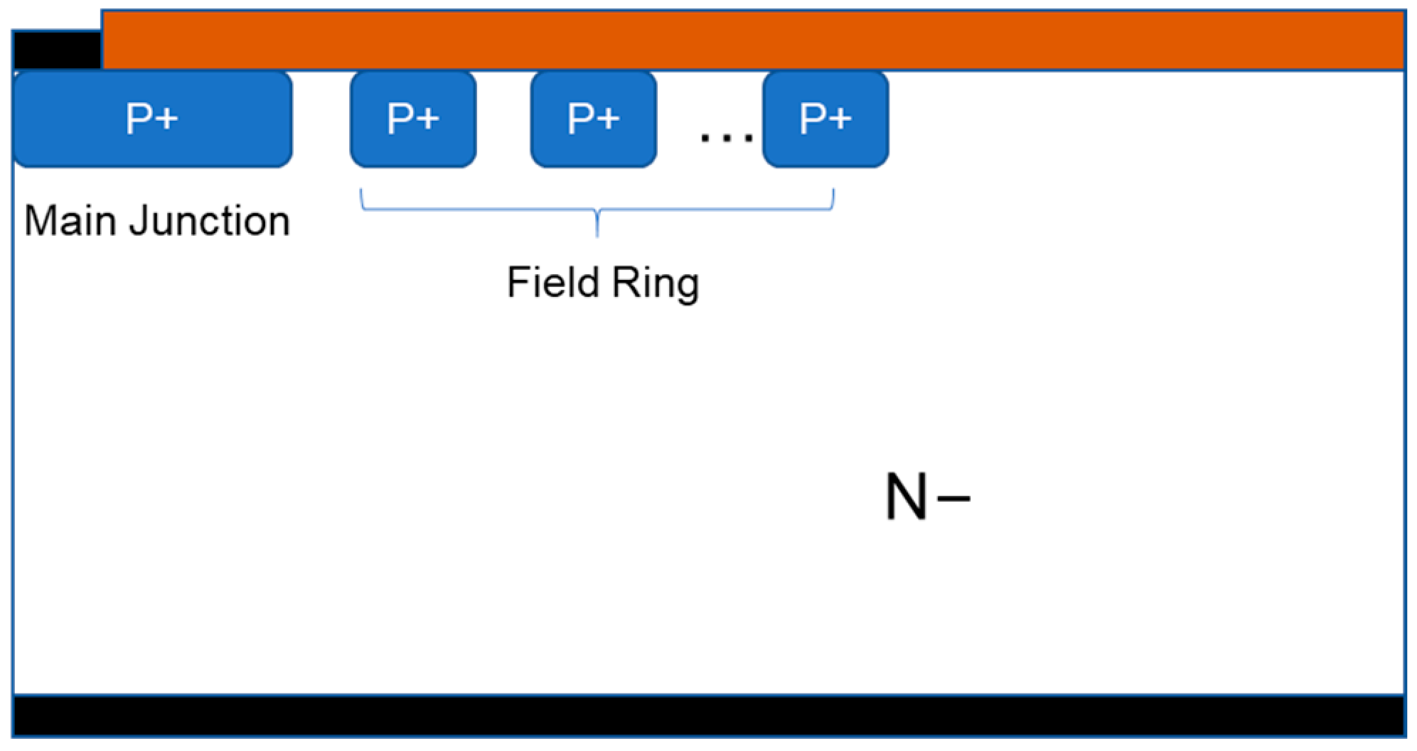
2.1. Device Under Testing
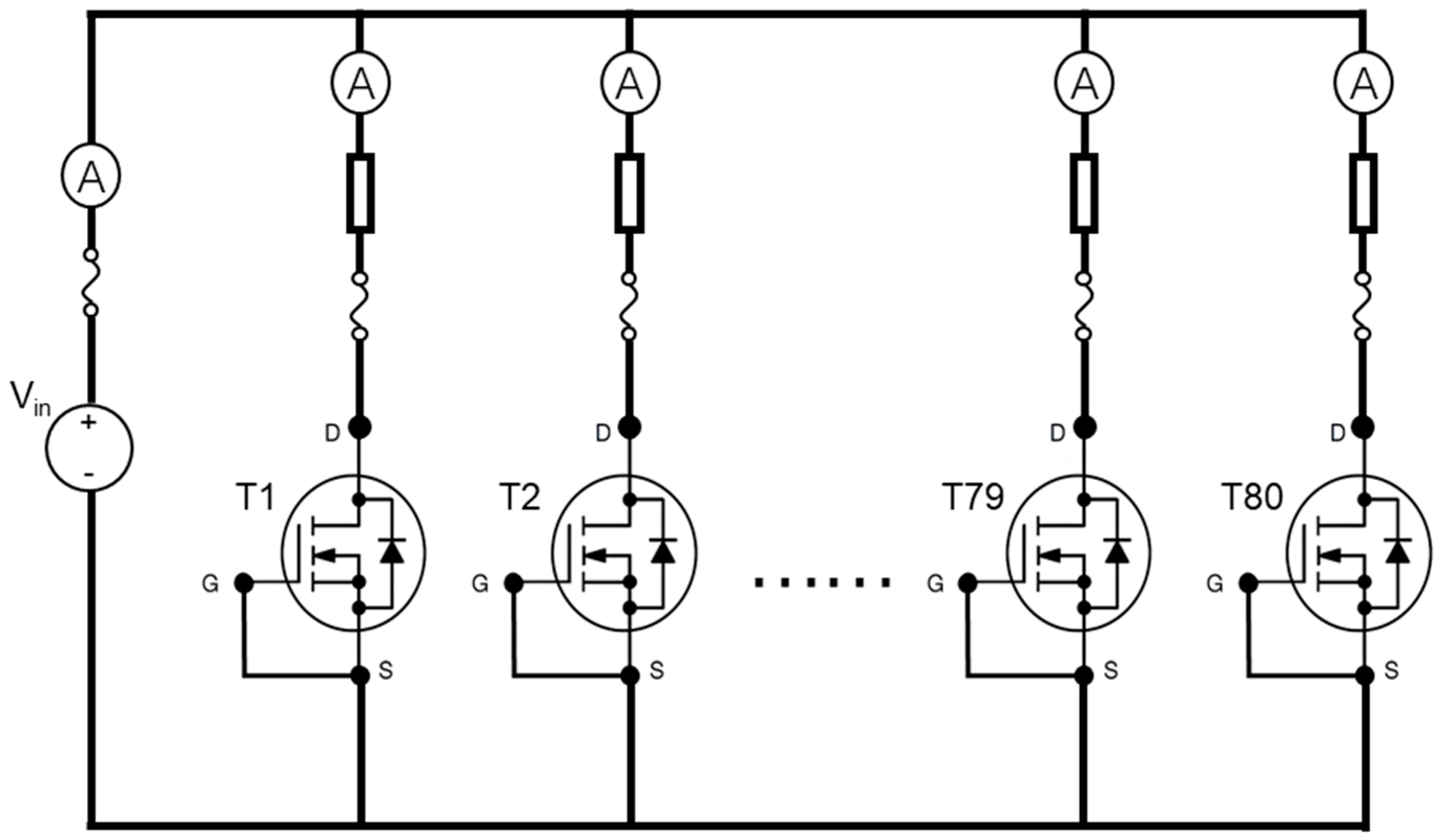
2.2. Experimental Conditions and Setup
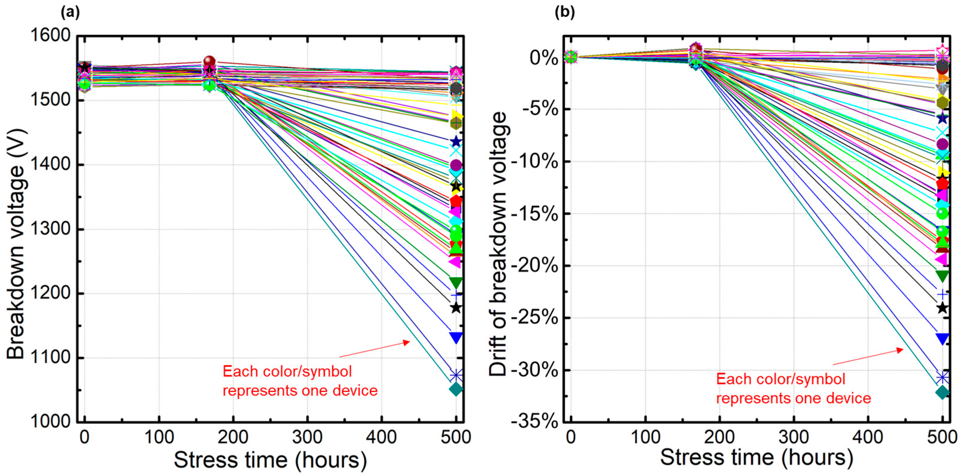
3. Results and Discussion
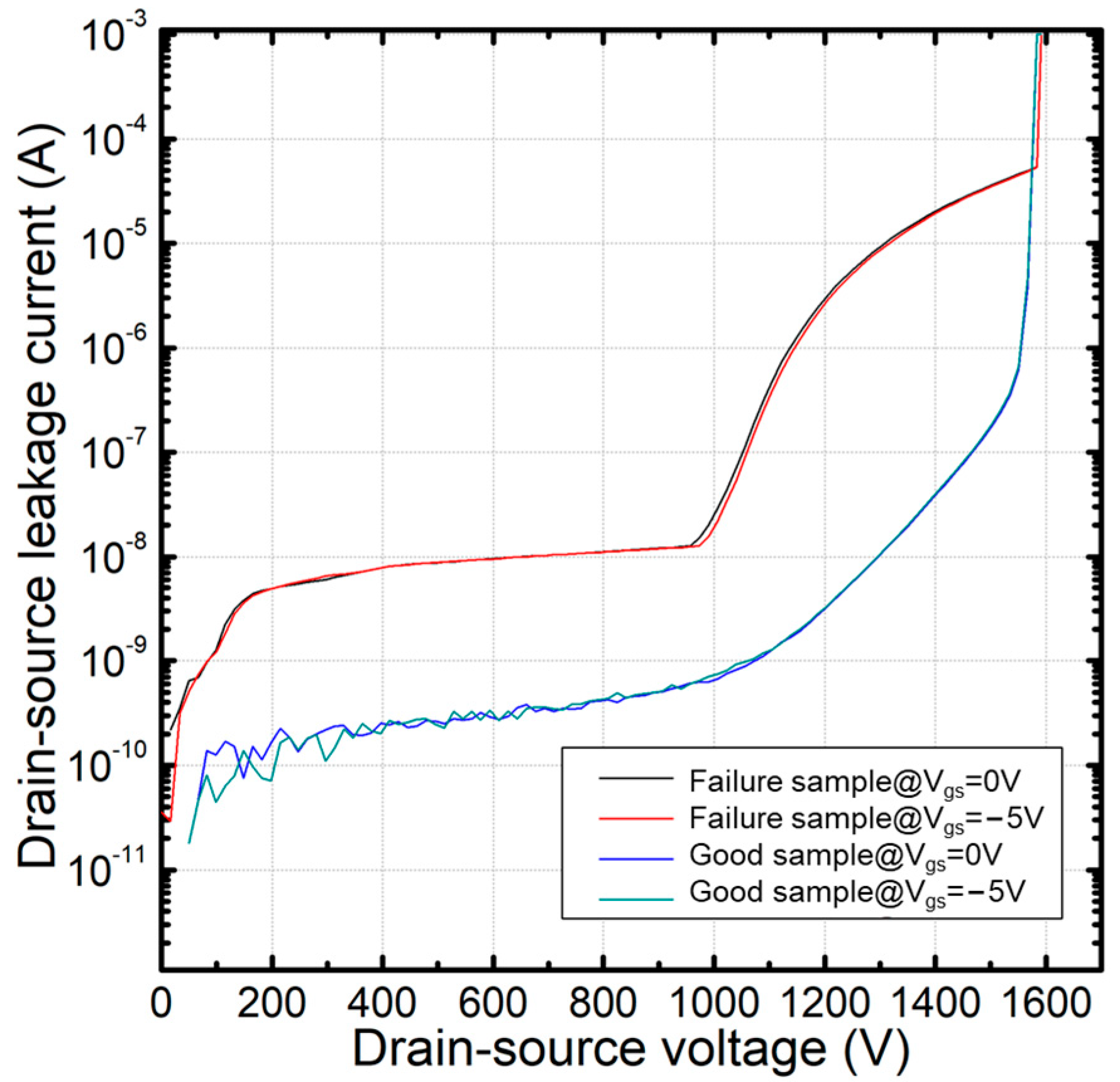
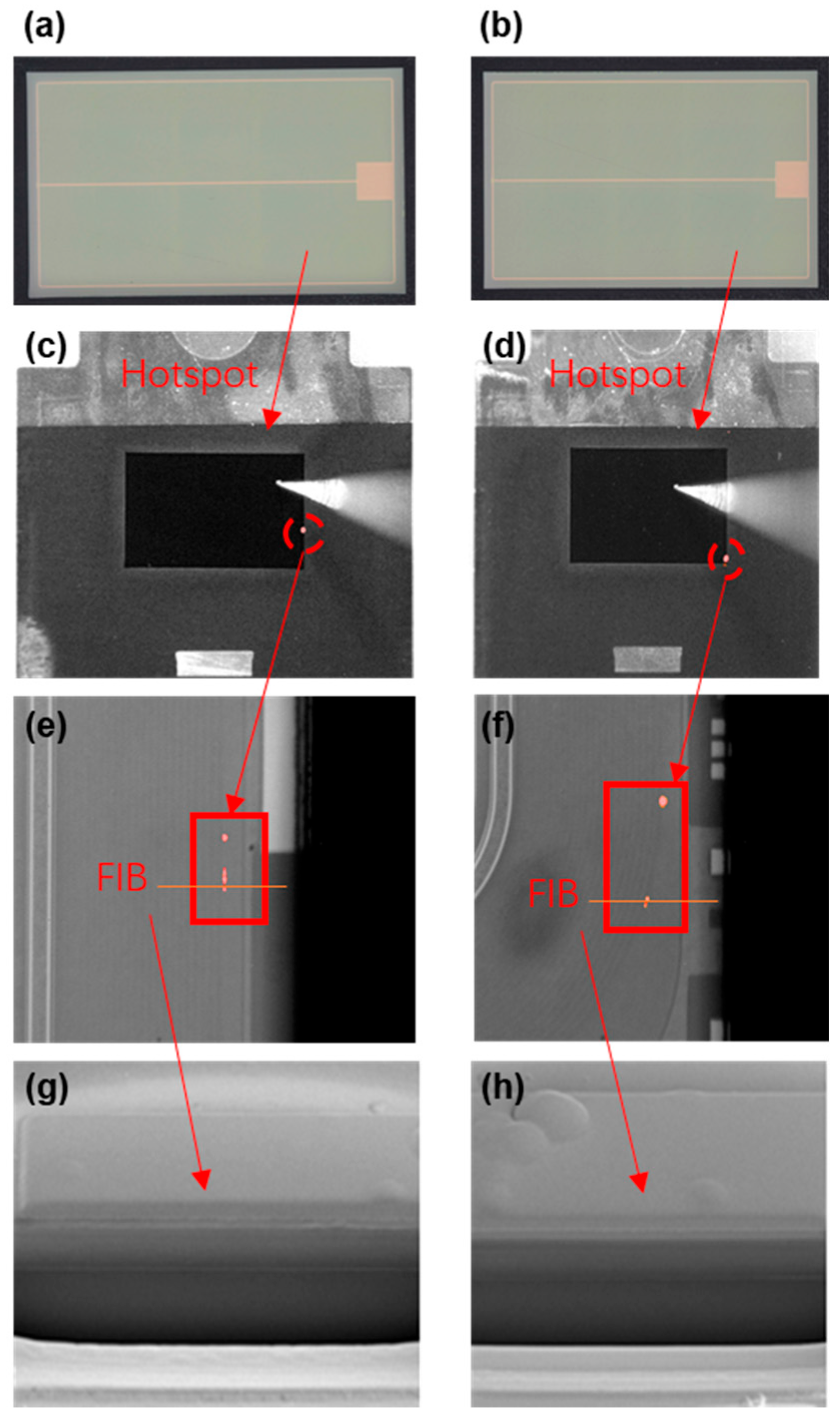
3.1. Device Failure Analysis
- The overall Idss leakage current of the failure sample is higher than that of the good sample;
- There is a sudden leakage current increase around 1000 V for the failure sample;
- The BV curves remain the same, regardless of whether the gate voltage is 0 V or −5 V.
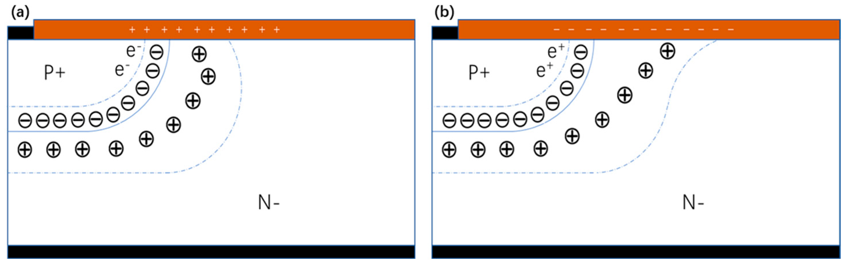
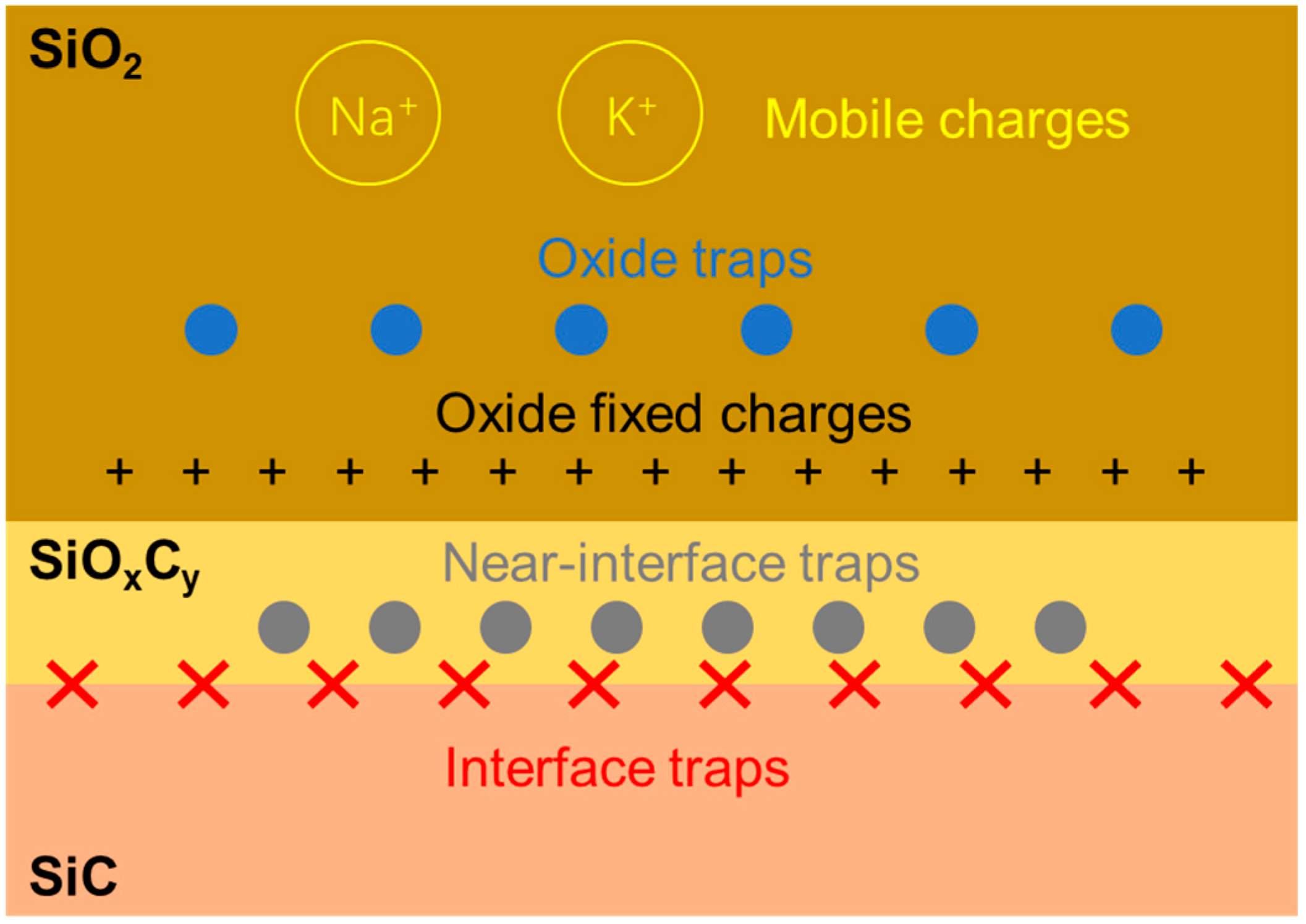
3.2. Failure Mechanism Discussion
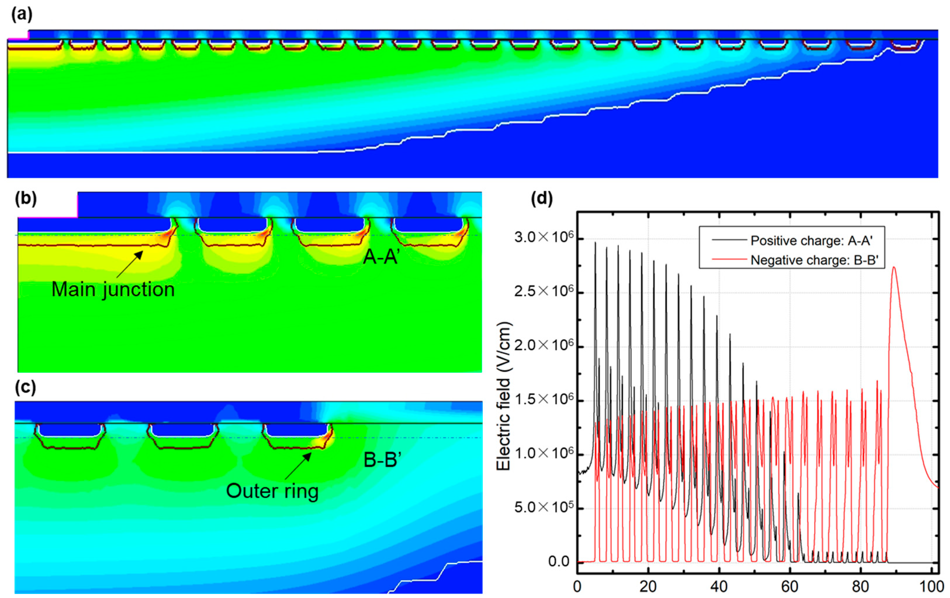
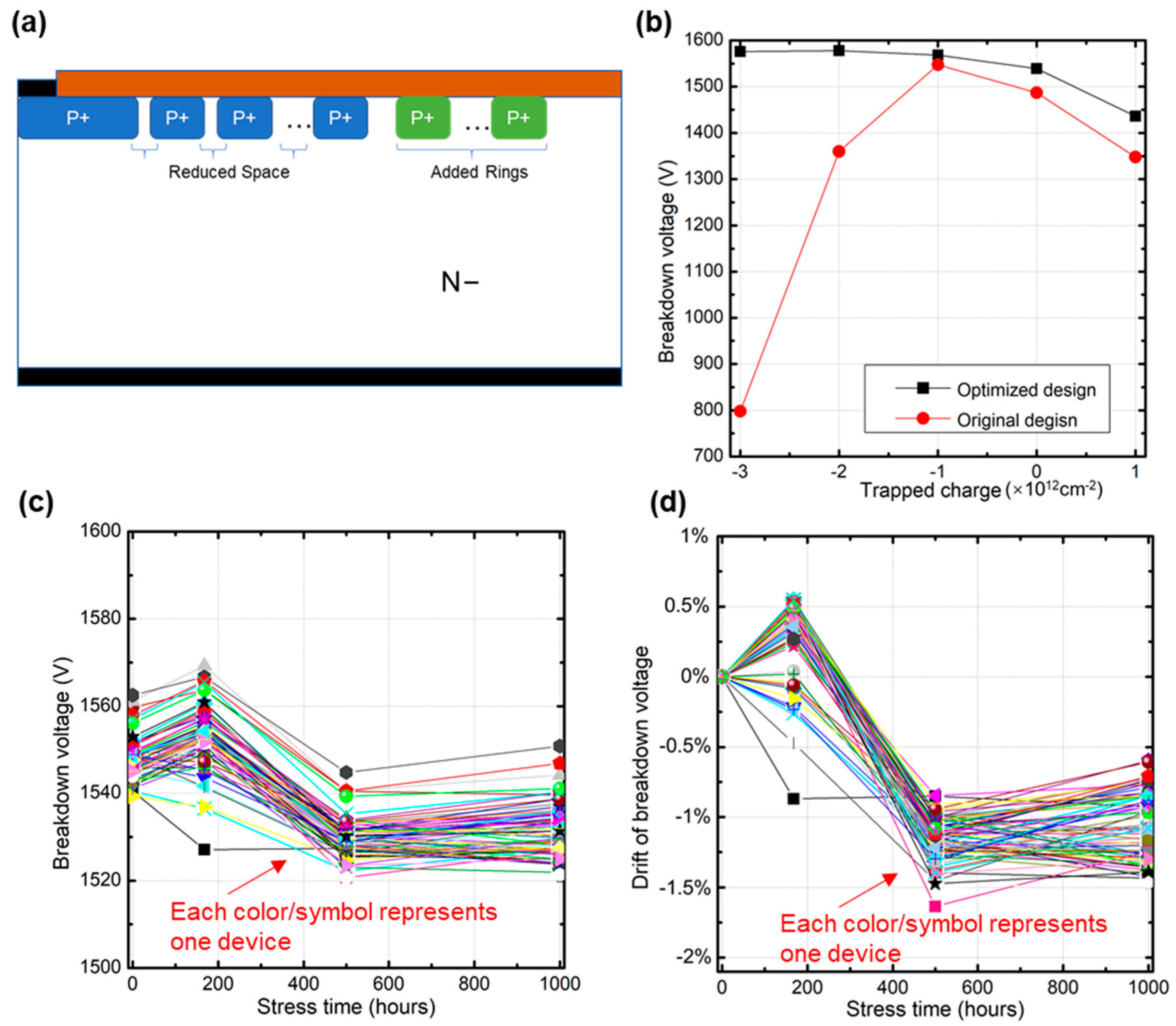
4. TCAD Simulation and Optimized Design
5. Conclusions
Author Contributions
Funding
Data Availability Statement
Conflicts of Interest
References
- Cooper, J.A.; Melloch, M.R.; Singh, R.; Agarwal, A.; Palmour, J.W. Status and prospects for SiC power MOSFETs. IEEE Trans. Electron Devices 2002, 49, 658–664. [Google Scholar] [CrossRef]
- Lucía, Ó.; She, X.; Huang, A.Q. Wide Bandgap Devices and Power Conversion Systems—Part II. IEEE Trans. Ind. Electron. 2017, 64, 8959–8961. [Google Scholar] [CrossRef]
- Kimoto, T.; Cooper, J.A. Physical Properties of Silicon Carbide. In Fundamentals of Silicon Carbide Technology: Growth, Characterization, Devices and Applications; IEEE: Piscataway, NJ, USA, 2014. [Google Scholar]
- Yuan, X.; Laird, I.; Walder, S. Opportunities, Challenges, and Potential Solutions in the Application of Fast-Switching SiC Power Devices and Converters. IEEE Trans. Power Electron. 2021, 36, 3925–3945. [Google Scholar] [CrossRef]
- Ji, S.; Zhang, Z.; Wang, F. Overview of high voltage sic power semiconductor devices: Development and application. CES Trans. Electr. Mach. Syst. 2017, 1, 254–264. [Google Scholar] [CrossRef]
- Kim, D.; Yun, N.; Jang, S.Y.; Morgan, A.J.; Sung, W. Channel Design Optimization for 1.2-kV 4H-SiC MOSFET Achieving Inherent Unipolar Diode 3rd Quadrant Operation. IEEE J. Electron Devices Soc. 2022, 10, 495–503. [Google Scholar] [CrossRef]
- Kumar, K.; Bertoluzzo, M.; Buja, G. Impact of SiC MOSFET traction inverters on compact-class electric car range. In Proceedings of the IEEE International Conference on Power Electronics, Drives and Energy Systems, Mumbai, India, 16–19 December 2014; pp. 1–6. [Google Scholar]
- Lee, J.S.; Chun, D.H.; Park, J.H.; Jung, Y.K.; Kang, E.G.; Sung, M.Y. Design of a novel SiC MOSFET structure for EV inverter efficiency improvement. In Proceedings of the IEEE International Symposium on Power Semiconductor Devices & IC’s, Waikoloa, HI, USA, 15–19 June 2014; pp. 281–284. [Google Scholar]
- Gurpinar, E.; Wiles, R.; Ozpineci, B.; Raminosoa, T.; Zhou, F.; Liu, Y.; Dede, E.M. SiC MOSFET-Based Power Module Design and Analysis for EV Traction Systems. In Proceedings of the IEEE Energy Conversion Congress and Exposition, Portland, OR, USA, 23–27 September 2018; pp. 1722–1727. [Google Scholar]
- Kim, H.; Chen, H.; Zhu, J.; Maksimovic, D.; Erickson, R. Impact of 1.2kV SiC-MOSFET EV traction inverter on urban driving. In Proceedings of the IEEE Workshop on Wide Bandgap Power Devices and Applications, Fayetteville, AR, USA, 7–9 November 2016; pp. 78–83. [Google Scholar]
- Sung, W.; Baliga, B.J. A Comparative Study 4500-V Edge Termination Techniques for SiC Devices. IEEE Trans. Electron Devices 2017, 64, 1647–1652. [Google Scholar] [CrossRef]
- Dai, T.; Zhang, L.; Vavasour, O.; Renz, A.B.; Cao, Q.; Shah, V.A.; Mawby, P.A.; Antoniou, M.; Gammon, P.M. A Compact and Cost-efficient Edge Termination Design for High Voltage 4H-SiC Devices. In Proceedings of the IEEE International Symposium on Power Semiconductor Devices and ICs, Nagoya, Japan, 30 May–3 June 2021; pp. 251–254. [Google Scholar]
- Yuan, H.; Liu, Y.; He, Y.; Hu, Y.; Zhang, T.; Tang, X.; Song, Q.; Zhang, Y.; Zhang, Y.; He, X.; et al. Characteristic and Robustness of Trench Floating Limiting Rings for 4H-SiC Junction Barrier Schottky Rectifiers. IEEE Electron Device Lett. 2020, 41, 1056–1059. [Google Scholar] [CrossRef]
- Liu, Y.; Feng, H.; Zhou, X.; Huang, L.; Xiao, C.; Peng, X.; Sin, J.K.O. A New Double Trench, Buried-P JTE Edge Termination for 1200 V-class SiC Devices. In Proceedings of the IEEE International Symposium on Power Semiconductor Devices and ICs, Vienna, Austria, 13–18 September 2020; pp. 162–165. [Google Scholar]
- Zhou, C.N.; Wang, Y.; Yue, R.F.; Dai, G.; Li, J.T. Step JTE, an Edge Termination for UHV SiC Power Devices With Increased Tolerances to JTE Dose and Surface Charges. IEEE Trans. Electron Devices 2017, 64, 1193–1196. [Google Scholar] [CrossRef]
- Deng, X.; Li, L.; Wu, J.; Li, C.; Chen, W.; Li, J.; Li, Z.; Zhang, B. A Multiple-Ring-Modulated JTE Technique for 4H-SiC Power Device With Improved JTE-Dose Window. IEEE Trans. Electron Devices 2017, 64, 5042–5047. [Google Scholar] [CrossRef]
- Mihaila, A.; Sundaramoorthy, V.K.; Minamisawa, R.; Knoll, L.; Bartolf, H.; Bianda, E.; Alfieri, G.; Rahimo, M. A novel edge termination for high voltage SiC devices. In Proceedings of the IEEE International Symposium on Power Semiconductor Devices and ICs, Prague, Czech Republic, 12–16 June 2016; pp. 223–226. [Google Scholar]
- Huang, C.F.; Hsu, H.C.; Chu, K.W.; Lee, L.H.; Tsai, M.J.; Lee, K.Y.; Zhao, F. Counter-Doped JTE, an Edge Termination for HV SiC Devices With Increased Tolerance to the Surface Charge. IEEE Trans. Electron Devices 2015, 62, 354–358. [Google Scholar] [CrossRef]
- Zhang, C.; Wang, H.; Wang, C.; Zhang, L.; Sheng, K. Termination Design of 6.5kV SiC MOSFET with Epitaxial Current Spreading Layer. In Proceedings of the IEEE International Forum on Wide Bandgap Semiconductors, Xiamen, China, 27–30 November 2023; pp. 92–95. [Google Scholar]
- Huang, L.; Cao, J.; Wang, C.; Fu, H.; Wei, J.; Liu, S.; Sun, W. High Performance Termination Design and Fabrication for SiC MOSFET Device. In Proceedings of the IEEE 17th International Conference on Solid-State & Integrated Circuit Technology, Zhuhai, China, 22–25 October 2024; pp. 1–3. [Google Scholar]
- Liu, Y.; Feng, H.; Peng, X.; Huang, L.; Sin, J.K.O. Experimental Demonstration of the Double-Trench, Buried-P JTE Edge Termination with Short Edge Width and High dV/dt Capability for 1200 V-class SiC Devices. In Proceedings of the IEEE 36th International Symposium on Power Semiconductor Devices and ICs, Bremen, Germany, 2–6 June 2024; pp. 17–20. [Google Scholar]
- Yuan, J.; Cheng, Z.; Guo, F.; Wang, K.; Chen, W.; Wu, Y.; Xu, S.; Xin, G.; Wang, Z. A Trench and Field Limiting Rings Co-Assisted JTE Termination With N-P-N Sandwich Epitaxial Wafers for 4H-SiC Devices. IEEE Electron Device Lett. 2024, 45, 1425–1428. [Google Scholar] [CrossRef]
- Singh, P.; Karmalkar, S.; Akshay, K. Humidity and ring spacing variation tolerant design of a SiC power MOSFET using mirrored floating field rings. Microelectron. J. 2025, 158, 106611. [Google Scholar] [CrossRef]
- Chbili, Z.; Matsuda, A.; Chbili, J.; Ryan, J.T.; Campbell, J.P.; Lahbabi, M.; Ioannou, D.E.; Cheung, K.P. Modeling Early Breakdown Failures of Gate Oxide in SiC Power MOSFETs. IEEE Trans. Electron Devices 2016, 63, 3605–3613. [Google Scholar] [CrossRef]
- Puschkarsky, K.; Grasser, T.; Aichinger, T.; Gustin, W.; Reisinger, H. Review on SiC MOSFETs High-Voltage Device Reliability Focusing on Threshold Voltage Instability. IEEE Trans. Electron Devices 2019, 66, 4604–4616. [Google Scholar] [CrossRef]
- Cheung, K.P. SiC power MOSFET gate oxide breakdown reliability—Current status. In Proceedings of the IEEE International Reliability Physics Symposium, Burlingame, CA, USA, 11–15 March 2018; pp. 2B.3-1–2B.3-5. [Google Scholar]
- Gajewski, D.A.; Hull, B.; Lichtenwalner, D.J.; Ryu, S.H.; Bonelli, E.; Mustain, H.; Wang, G.; Allen, S.T.; Palmour, J.W. SiC power device reliability. In Proceedings of the IEEE International Integrated Reliability Workshop, South Lake Tahoe, CA, USA, 9–13 October 2016; pp. 29–34. [Google Scholar]
- Hull, B.; Allen, S.; Zhang, Q.; Gajewski, D.; Pala, V.; Richmond, J.; Ryu, S.; O’Loughlin, M.; Van Brunt, E.; Cheng, L.; et al. Reliability and stability of SiC power mosfets and next-generation SiC MOSFETs. In Proceedings of the IEEE Workshop on Wide Bandgap Power Devices and Applications, Knoxville, TN, USA, 13–15 October 2014; pp. 139–142. [Google Scholar]
- Habersat, D.B.; Lelis, A.J.; Green, R. Towards a Robust Approach to Threshold Voltage Characterization and High Temperature Gate Bias Qualification. In Proceedings of the IEEE International Reliability Physics Symposium, Dallas, TX, USA, 28 April–30 May 2020; pp. 1–4. [Google Scholar]
- Afanasev, V.V.; Bassler, M.; Pensl, G.; Schulz, M. Intrinsic SiC/SiO2 Interface States. Phys. Status Solidi (a) 1997, 162, 321–337. [Google Scholar] [CrossRef]
- Fujino, Y.; Kita, K. Quantitative Characterization of Near-Interface Oxide Traps in 4H-SiC MOS Capacitors by Transient Capacitance Measurements. In Proceedings of the 228th ECS Meeting, Phoenix, AZ, USA, 11–15 October 2015; The Electrochemical Society: Pennington, NJ, USA, 2015. [Google Scholar]
- Zhang, X.; Okamoto, D.; Hatakeyama, T.; Sometani, M.; Harada, S.; Kosugi, R.; Iwamuro, N.; Yano, H. Characterization of near-interface traps at 4H-SiC metal–oxide–semiconductor interfaces using modified distributed circuit model. Appl. Phys. Express 2017, 10, 064101. [Google Scholar] [CrossRef]
- Fiorenza, P.; Giannazzo, F.; Roccaforte, F. Characterization of SiO2/4H-SiC Interfaces in 4H-SiC MOSFETs: A Review. Energies 2019, 12, 2310. [Google Scholar] [CrossRef]
- Cuong, V.V.; Koyanagi, K.; Meguro, T.; Ishikawa, S.; Maeda, T.; Sezaki, H.; Kuroki, S.I. Study of interface-trap and near-interface-state distribution in a 4H-SiC MOS capacitor with the full-distributed circuit model. Jpn. J. Appl. Phys. 2024, 63, 015503. [Google Scholar] [CrossRef]


| Item | Test Condition | Value |
|---|---|---|
| Igss | Vgs = 25 V, Vds = 0 V | 4 nA |
| Idss | Vds = 1400 V, Vgs = 0 V | 17 nA |
| Vth | Vgs = Vds, Id = 20 mA | 2.8 V |
| Rdson | Vgs = 18 V, Id = 60 A | 17 mΩ |
| BVDSS | Vgs = 0 V, Id = 5 uA | 1540 V |
| Main Parameters | Value |
|---|---|
| Drain voltage | 1200 V |
| Gate voltage | 0 V |
| Test temperature | 175 °C |
| Test number | ≥77 pcs |
| Test lot | 3 lots |
| Test duration | 1000 h |
Disclaimer/Publisher’s Note: The statements, opinions and data contained in all publications are solely those of the individual author(s) and contributor(s) and not of MDPI and/or the editor(s). MDPI and/or the editor(s) disclaim responsibility for any injury to people or property resulting from any ideas, methods, instructions or products referred to in the content. |
© 2025 by the authors. Licensee MDPI, Basel, Switzerland. This article is an open access article distributed under the terms and conditions of the Creative Commons Attribution (CC BY) license (https://creativecommons.org/licenses/by/4.0/).
Share and Cite
Yu, M.; Shen, Y.; Ma, H.; Zhang, Q. Experiment and Analysis of Termination Robustness Design for 1200 V 4H-SiC MOSFET. Nanomaterials 2025, 15, 805. https://doi.org/10.3390/nano15110805
Yu M, Shen Y, Ma H, Zhang Q. Experiment and Analysis of Termination Robustness Design for 1200 V 4H-SiC MOSFET. Nanomaterials. 2025; 15(11):805. https://doi.org/10.3390/nano15110805
Chicago/Turabian StyleYu, Mengyuan, Yi Shen, Hongping Ma, and Qingchun Zhang. 2025. "Experiment and Analysis of Termination Robustness Design for 1200 V 4H-SiC MOSFET" Nanomaterials 15, no. 11: 805. https://doi.org/10.3390/nano15110805
APA StyleYu, M., Shen, Y., Ma, H., & Zhang, Q. (2025). Experiment and Analysis of Termination Robustness Design for 1200 V 4H-SiC MOSFET. Nanomaterials, 15(11), 805. https://doi.org/10.3390/nano15110805