

Electrical Transport Interplay with Charge Density Waves, Magnetization, and Disorder Tuned by 2D van der Waals Interface Modification via Elemental Intercalation and Substitution in ZrTe3, 2H-TaS2, and Cr2Si2Te6 Crystals


Abstract
1. Introduction
2. Electrical Transport Properties in Doped ZrTe3 [128,129]
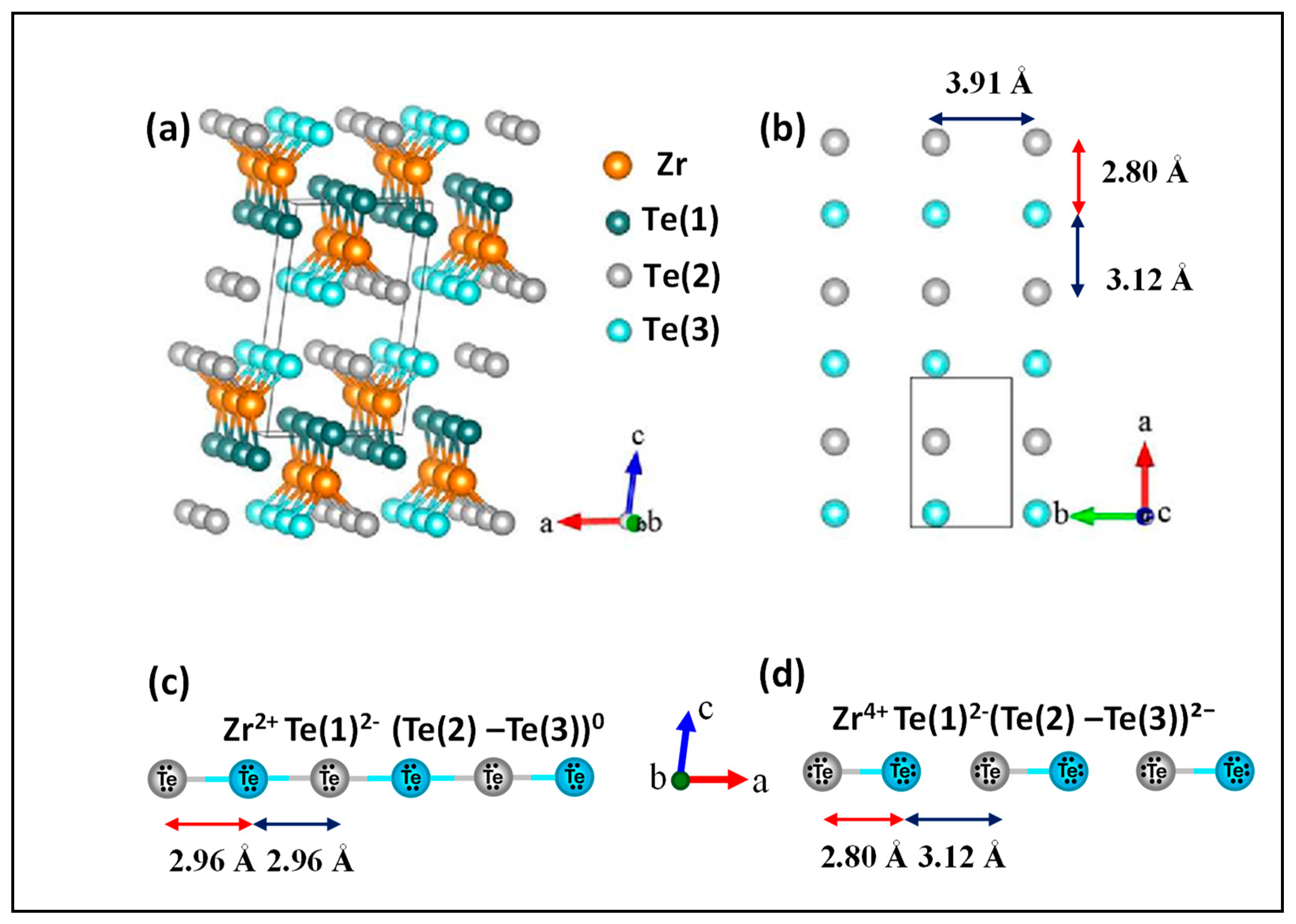
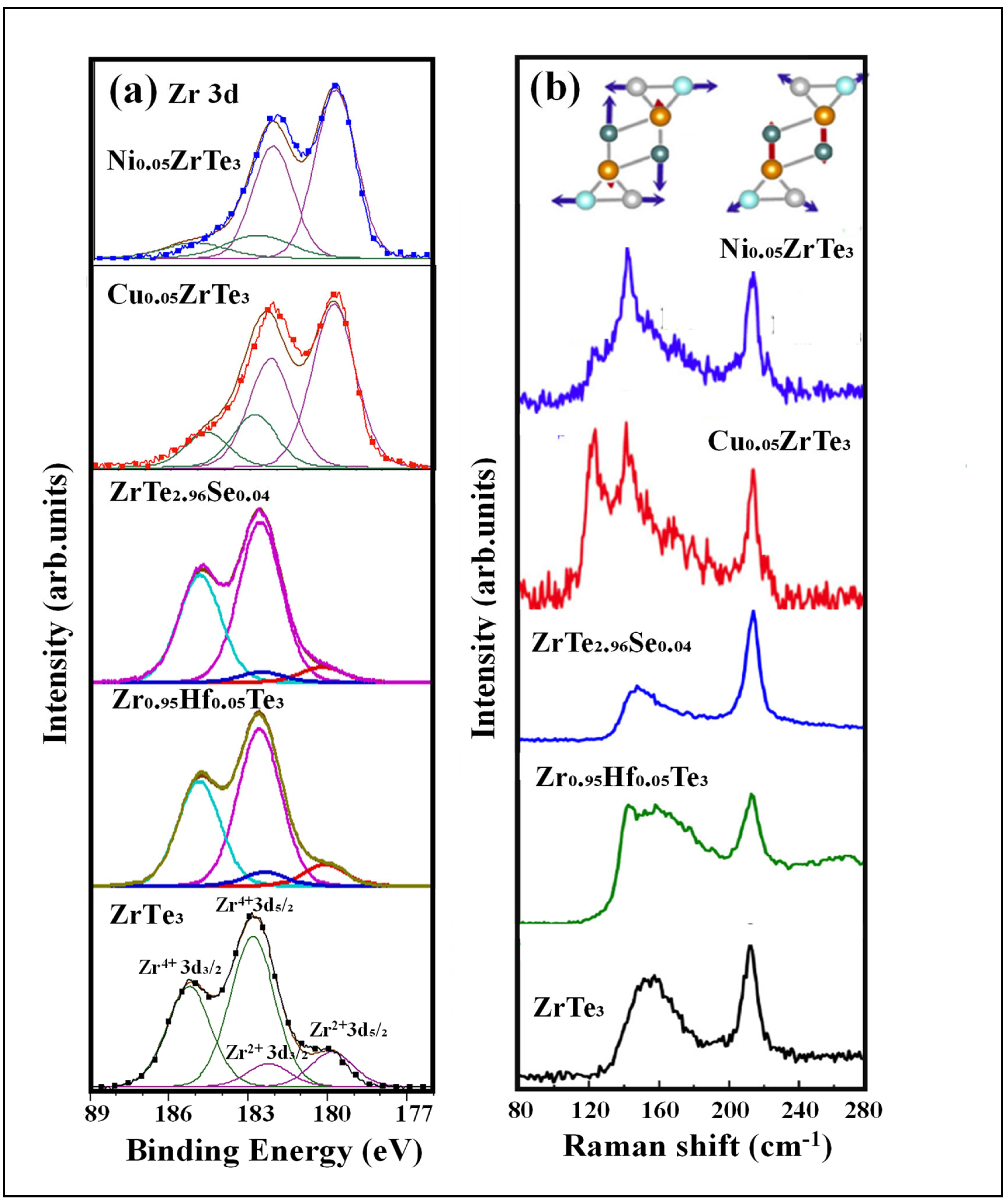
2.1. Dopant-Modulated Crystal Structures and Valence States
2.2. Dopant-Modulated Vibrational Structures
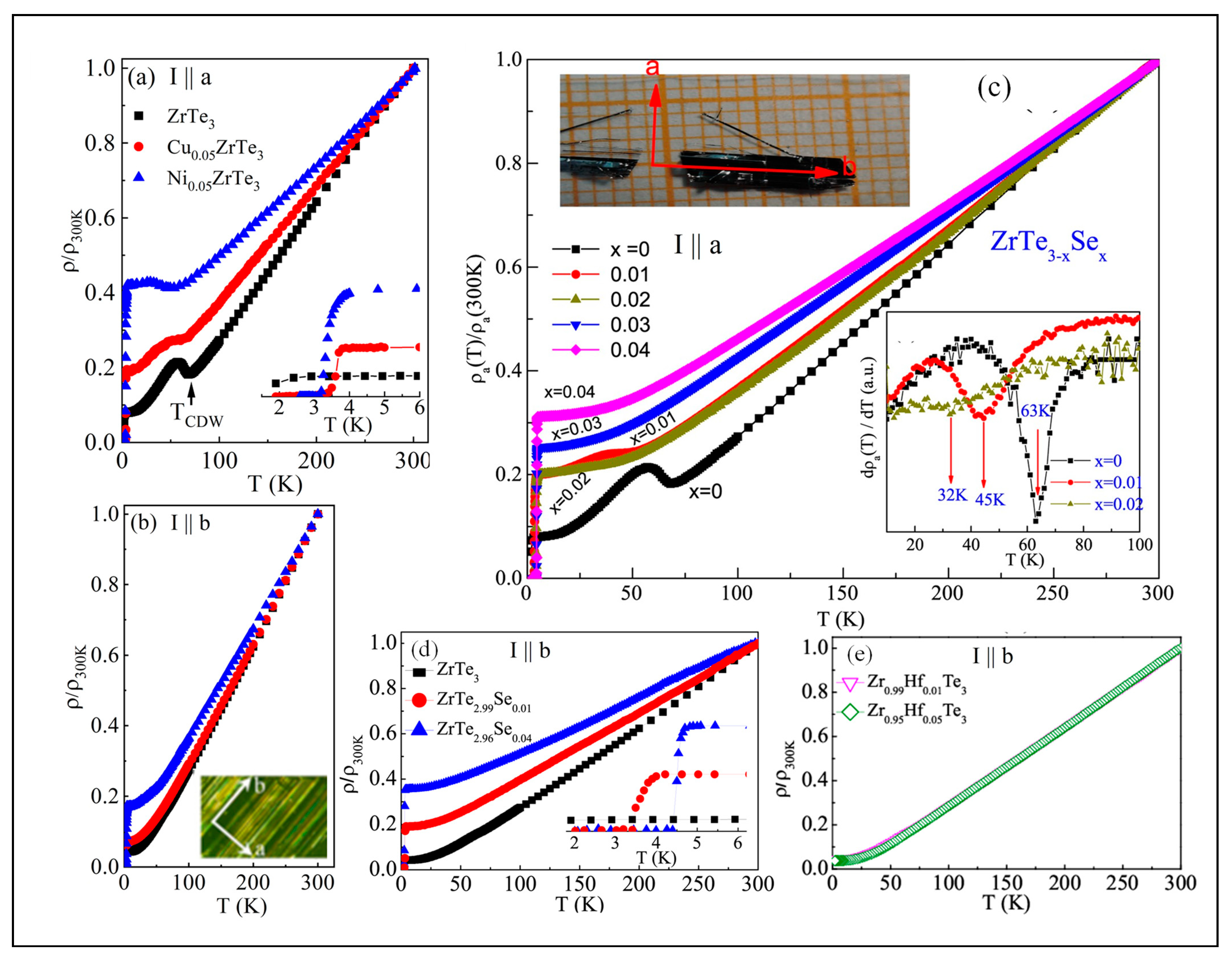
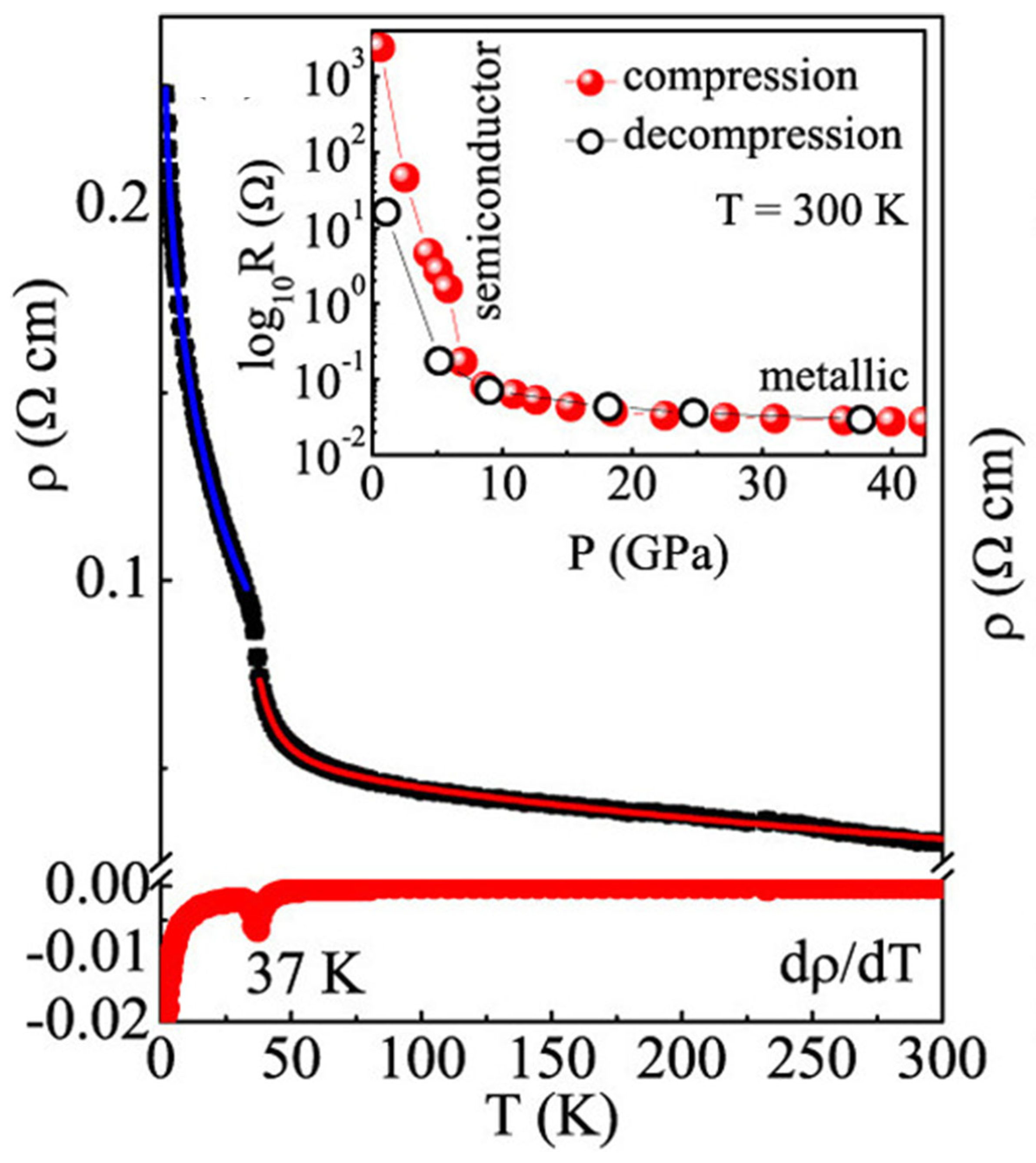
2.3. Interplay Among Electron–Phonon Coupling, CDW, and Electrical Transport
2.4. New Insights into the Superconductivity Mechanism of ZrTe3
- In the bulk: 2Zr3+ ↔ Zr2+ + Zr4+;
- In the quasi-1D lattice: 2(Te(2)-Te(3))1− ↔ (Te(2)-Te(3))2− + (Te(2)-Te(3))0.
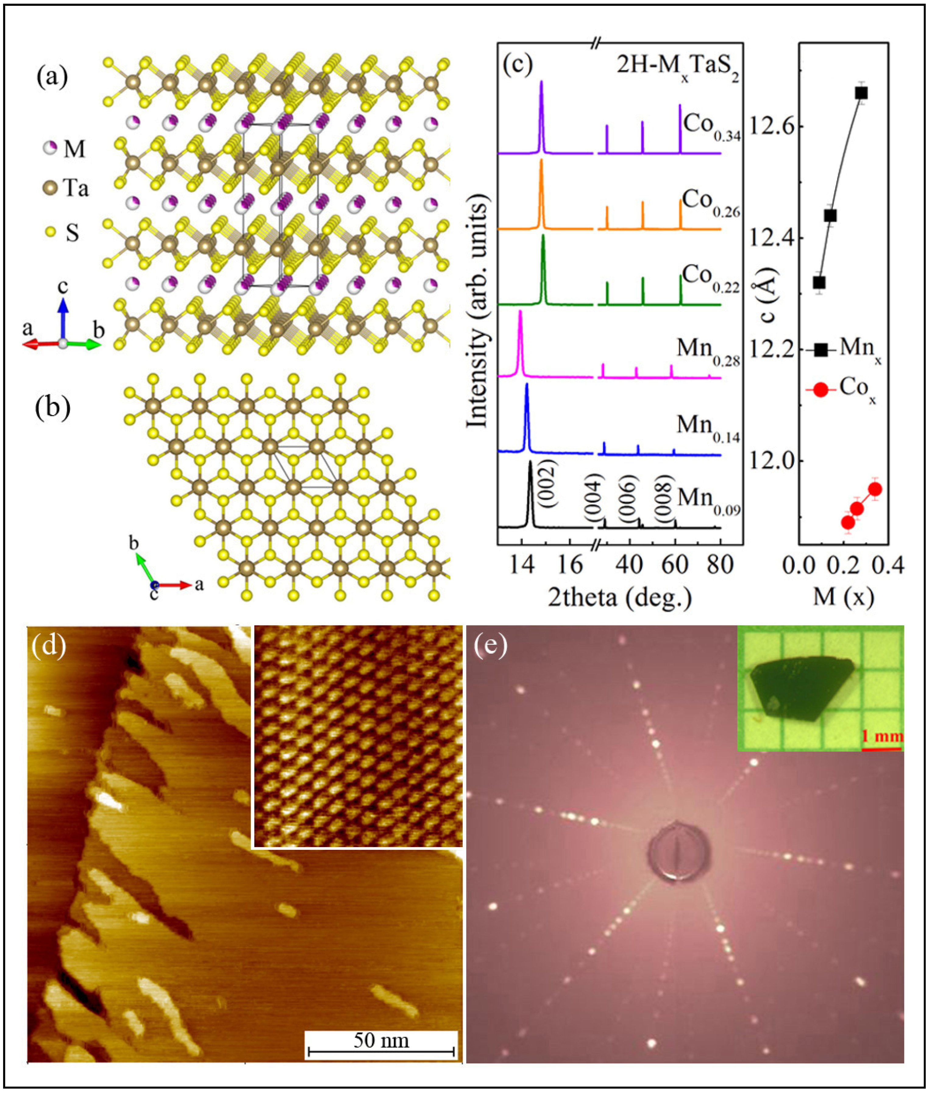
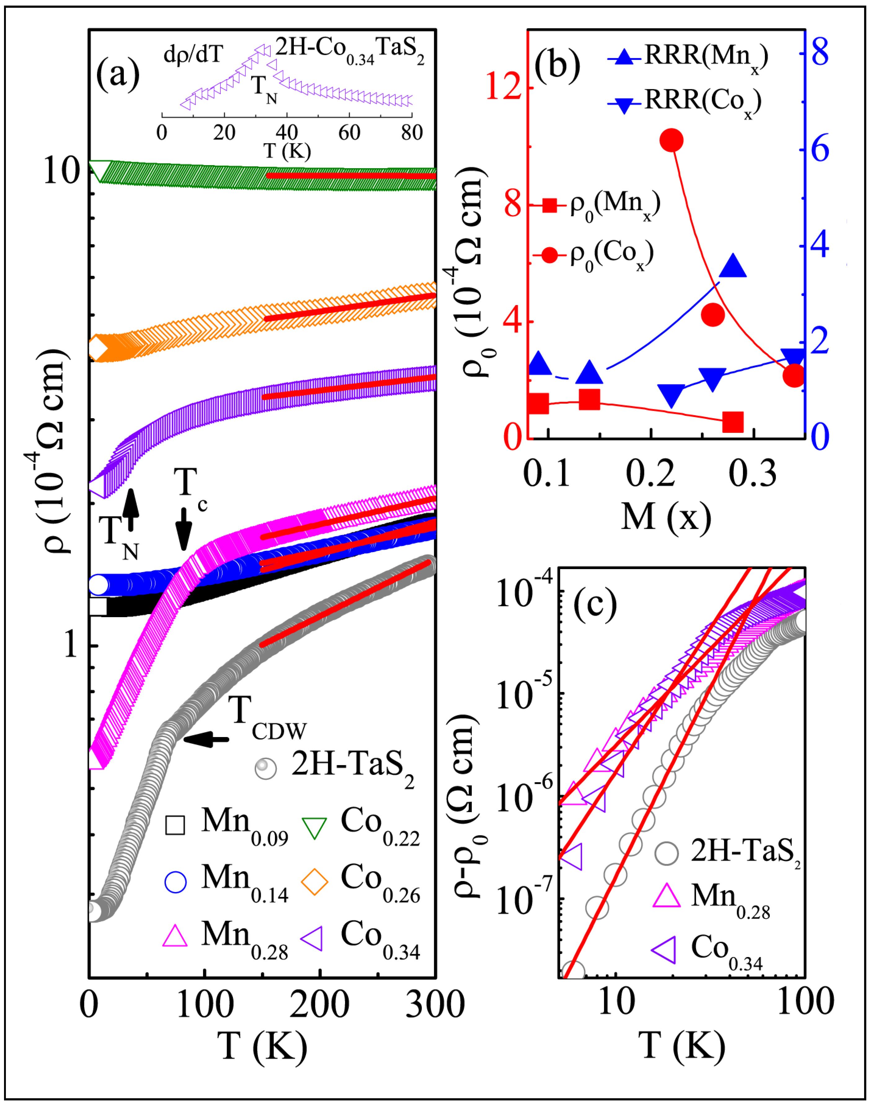
3. Electrical Transport in vdW Magnets: 2H-MxTaS2 (M = Mn, Co) [131]
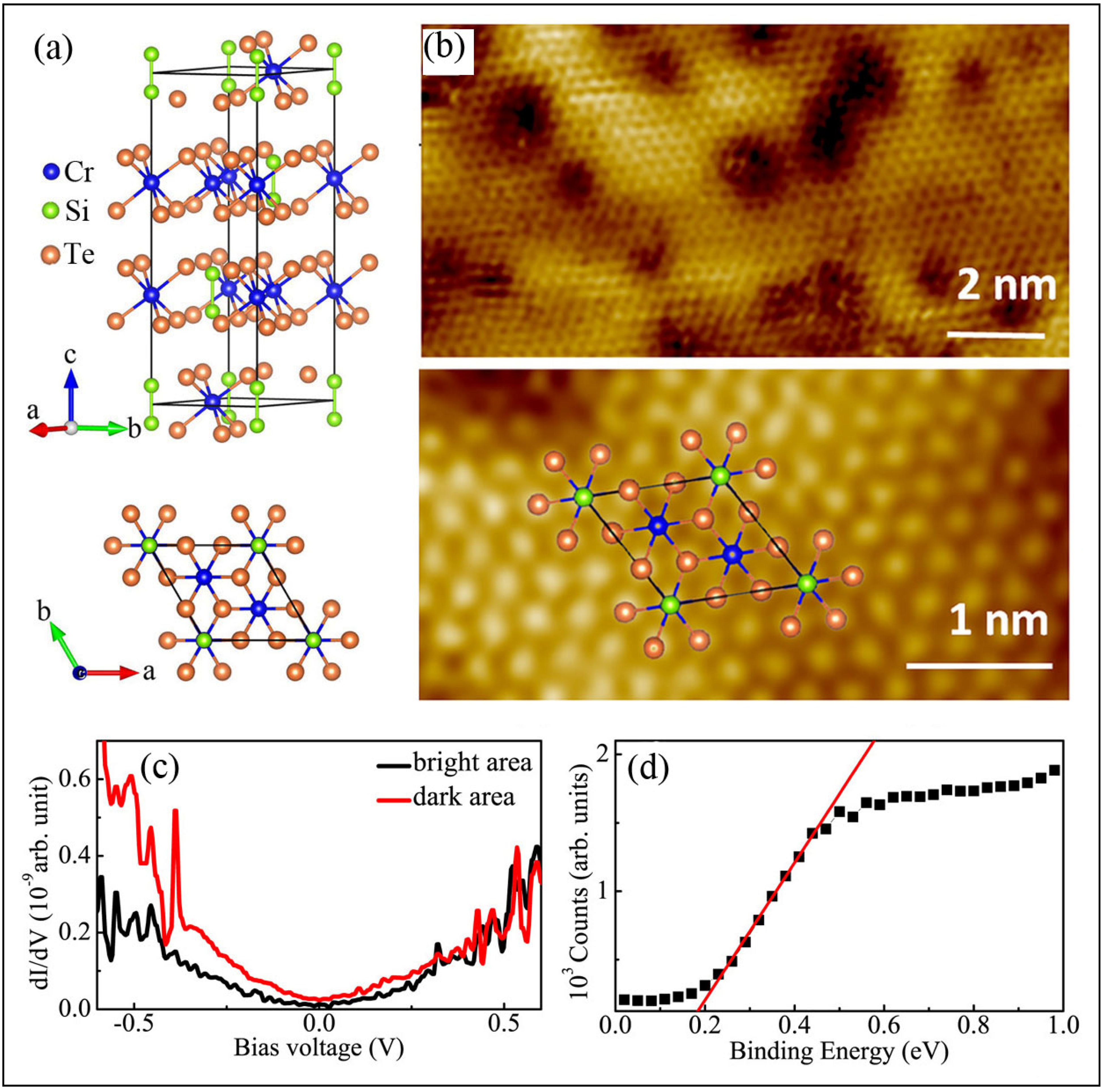
4. Short-Range Crystalline Order-Tuned Conductivity in Cr2Si2Te6 vdW Magnetic Crystals [130]
5. Future Directions
6. Conclusions
Funding
Conflicts of Interest
References
- Novoselov, K.S.; Geim, A.K.; Morozov, S.V.; Jiang, D.; Zhang, Y.; Dubonos, S.V.; Grigorieva, I.V.; Firsov, A.A. Electric field effect in atomically thin carbon films. Science 2004, 306, 666–669. [Google Scholar] [CrossRef] [PubMed]
- Wilson, N.P.; Yao, W.; Shan, J.; Xu, X.D. Excitons and emergent quantum phenomena in stacked 2D semiconductors. Nature 2021, 599, 383–392. [Google Scholar] [CrossRef] [PubMed]
- Li, J.; Yang, X.D.; Liu, Y.; Huang, B.L.; Wu, R.X.; Zhang, Z.W.; Zhao, B.; Ma, H.F.; Dang, W.Q.; Wei, Z.; et al. General synthesis of two-dimensional van der Waals heterostructure arrays. Nature 2020, 579, 368–374. [Google Scholar] [CrossRef] [PubMed]
- Geim, A.K.; Novoselov, K.S. The rise of graphene. Nat. Mater. 2007, 6, 183–191. [Google Scholar] [CrossRef]
- Zhang, Y.J.; Ideue, T.; Onga, M.; Qin, F.; Suzuki, R.; Zak, A.; Tenne, R.; Smet, J.H.; Iwasa, Y. Enhanced intrinsic photovoltaic effect in tungsten disulfide nanotubes. Nature 2019, 570, 349–353. [Google Scholar] [CrossRef]
- Kang, K.; Xie, S.E.; Huang, L.J.; Han, Y.M.; Huang, P.Y.; Mak, K.F.; Kim, C.J.; Muller, D.; Park, J. High-mobility three-atom-thick semiconducting films with wafer-scale homogeneity. Nature 2015, 520, 656–660. [Google Scholar] [CrossRef]
- Liu, L.; Li, T.T.; Ma, L.; Li, W.S.; Gao, S.; Sun, W.J.; Dong, R.K.; Zou, X.L.; Fan, D.X.; Shao, L.W.; et al. Uniform nucleation and epitaxy of bilayer molybdenum disulfide on sapphire. Nature 2022, 605, 69–75. [Google Scholar] [CrossRef]
- Imada, M.; Fujimori, A.; Tokura, Y. Metal-insulator transitions. Rev. Mod. Phys. 1998, 70, 1039–1263. [Google Scholar] [CrossRef]
- Kane, C.L.; Mele, E.J. Quantum spin Hall effect in graphene. Phys. Rev. Lett. 2005, 95, 226801. [Google Scholar] [CrossRef]
- Gall, V.; Kraft, R.; Gornyi, I.V.; Danneau, R. Spin and valley degrees of freedom in a bilayer graphene quantum point contact: Zeeman splitting and interaction effects. Phys. Rev. Res. 2022, 4, 023142. [Google Scholar] [CrossRef]
- Novoselov, K.S.; Geim, A.K.; Morozov, S.V.; Jiang, D.; Katsnelson, M.I.; Grigorieva, I.V.; Dubonos, S.V.; Firsov, A.A. Two-dimensional gas of massless Dirac fermions in graphene. Nature 2005, 438, 197–200. [Google Scholar] [CrossRef] [PubMed]
- Zhang, Y.B.; Tan, Y.W.; Stormer, H.L.; Kim, P. Experimental observation of the quantum Hall effect and Berry’s phase in graphene. Nature 2005, 438, 201–204. [Google Scholar] [CrossRef] [PubMed]
- Iordanidou, K.; Mitra, R.; Shetty, N.; Lara-Avila, S.; Dash, S.; Kubatkin, S.; Wiktor, J. Electric Field and Strain Tuning of 2D Semiconductor van der Waals Heterostructures for Tunnel Field-Effect Transistors. ACS Appl. Mater. Interfaces 2023, 15, 1762–1771. [Google Scholar] [CrossRef]
- Chaves, A.; Azadani, J.G.; Alsalman, H.; da Costa, D.R.; Frisenda, R.; Chaves, A.J.; Song, S.H.; Kim, Y.D.; He, D.W.; Zhou, J.D.; et al. Bandgap engineering of two-dimensional semiconductor materials. npj 2D Mater. Appl. 2020, 4, 29. [Google Scholar] [CrossRef]
- Boland, C.S.; Sun, Y.W.; Papageorgiou, D.G. Bandgap Engineering of 2D Materials toward High-Performing Straintronics. Nano Lett. 2024, 24, 12722–12732. [Google Scholar] [CrossRef]
- Cao, Y.; Fatemi, V.; Fang, S.; Watanabe, K.; Taniguchi, T.; Kaxiras, E.; Jarillo-Herrero, P. Unconventional superconductivity in magic-angle graphene superlattices. Nature 2018, 556, 43–50. [Google Scholar] [CrossRef]
- Guo, Y.; Pack, J.; Swann, J.; Holtzman, L.; Cothrine, M.; Watanabe, K.; Taniguchi, T.; Mandrus, D.G.; Barmak, K.; Hone, J.; et al. Superconductivity in 5.0 degrees twisted bilayer WSe(2). Nature 2025, 637, 839–845. [Google Scholar] [CrossRef]
- Hasan, M.Z.; Kane, C.L. Colloquium: Topological insulators. Rev. Mod. Phys. 2010, 82, 3045–3067. [Google Scholar] [CrossRef]
- van der Zande, A.M.; Kunstrnann, J.; Chernikov, A.; Chenet, D.A.; You, Y.M.; Zhang, X.X.; Huang, P.Y.; Berkelbach, T.C.; Wang, L.; Zhang, F.; et al. Tailoring the Electronic Structure in Bilayer Molybdenum Disulfide via Interlayer Twist. Nano Lett. 2014, 14, 3869–3875. [Google Scholar] [CrossRef]
- Lee, J.; Mak, K.F.; Shan, J. Electrical control of the valley Hall effect in bilayer MoS transistors. Nat. Nanotechnol. 2016, 11, 421–425. [Google Scholar] [CrossRef]
- Xiao, D.; Liu, G.B.; Feng, W.X.; Xu, X.D.; Yao, W. Coupled Spin and Valley Physics in Monolayers of MoS and Other Group-VI Dichalcogenides. Phys. Rev. Lett. 2012, 108, 196802. [Google Scholar] [CrossRef] [PubMed]
- Soluyanov, A.A.; Gresch, D.; Wang, Z.J.; Wu, Q.S.; Troyer, M.; Dai, X.; Bernevig, B.A. Type-II Weyl semimetals. Nature 2015, 527, 495–498. [Google Scholar] [CrossRef] [PubMed]
- Mourik, V.; Zuo, K.; Frolov, S.M.; Plissard, S.R.; Bakkers, E.P.A.M.; Kouwenhoven, L.P. Signatures of Majorana Fermions in Hybrid Superconductor-Semiconductor Nanowire Devices. Science 2012, 336, 1003–1007. [Google Scholar] [CrossRef] [PubMed]
- Li, L.; Huang, T.; Liang, K.; Si, Y.; Lian, J.C.; Huang, W.Q.; Hu, W.Y.; Huang, G.F. Symmetry-Breaking-Induced Multifunctionalities of Two-Dimensional Chromium-Based Materials for Nanoelectronics and Clean Energy Conversion. Phys. Rev. Appl. 2022, 18, 014013. [Google Scholar] [CrossRef]
- Shi, Y.Y.; Groven, B.; Serron, J.; Wu, X.Y.; Mehta, A.N.; Minj, A.; Sergeant, S.; Han, H.; Asselberghs, I.; Lin, D.; et al. Engineering Wafer-Scale Epitaxial Two-Dimensional Materials through Sapphire Template Screening for Advanced High-Performance Nanoelectronics. ACS Nano 2021, 15, 9482–9494. [Google Scholar] [CrossRef]
- Kilic, M.E.; Lee, K.R. Tetrahex carbides: Two-dimensional group-IV materials for nanoelectronics and photocatalytic water splitting. Carbon 2021, 174, 368–381. [Google Scholar] [CrossRef]
- Sopiha, K.V.; Malyi, O.I.; Persson, C. First-Principles Mapping of the Electronic Properties of Two-Dimensional Materials for Strain-Tunable Nanoelectronics. ACS Appl. Nano Mater. 2019, 2, 5614–5624. [Google Scholar] [CrossRef]
- Liu, Z.; Wang, H.D.; Sun, J.Y.; Sun, R.J.; Wang, Z.F.; Yang, J.L. Penta-PtN: An ideal two-dimensional material for nanoelectronics. Nanoscale 2018, 10, 16169–16177. [Google Scholar] [CrossRef]
- Molle, A. Xenes: A new emerging two-dimensional materials platform for nanoelectronics. Semicond. Dielectr. Met. Nanoelectron. 14 2016, 75, 163–173. [Google Scholar] [CrossRef]
- Akinwande, D.; Petrone, N.; Hone, J. Two-dimensional flexible nanoelectronics. Nat. Commun. 2014, 5, 5678. [Google Scholar] [CrossRef]
- Liu, Y.; Weiss, N.O.; Duan, X.D.; Cheng, H.C.; Huang, Y.; Duan, X.F. Van der Waals heterostructures and devices. Nat. Rev. Mater. 2016, 1, 16042. [Google Scholar] [CrossRef]
- Evaldsson, M.; Zozoulenko, I.V.; Xu, H.Y.; Heinzel, T. Edge-disorder-induced Anderson localization and conduction gap in graphene nanoribbons. Phys. Rev. B 2008, 78, 161407. [Google Scholar] [CrossRef]
- Du, X.; Skachko, I.; Duerr, F.; Luican, A.; Andrei, E.Y. Fractional quantum Hall effect and insulating phase of Dirac electrons in graphene. Nature 2009, 462, 192–195. [Google Scholar] [CrossRef] [PubMed]
- Mak, K.F.; He, K.L.; Lee, C.; Lee, G.H.; Hone, J.; Heinz, T.F.; Shan, J. Tightly bound trions in monolayer MoS. Nat. Mater. 2013, 12, 207–211. [Google Scholar] [CrossRef]
- Mak, K.F.; He, K.L.; Shan, J.; Heinz, T.F. Control of valley polarization in monolayer MoS by optical helicity. Nat. Nanotechnol. 2012, 7, 494–498. [Google Scholar] [CrossRef]
- Xu, S.Y.; Belopolski, I.; Alidoust, N.; Neupane, M.; Bian, G.; Zhang, C.L.; Sankar, R.; Chang, G.Q.; Yuan, Z.J.; Lee, C.C.; et al. Discovery of a Weyl fermion semimetal and topological Fermi arcs. Science 2015, 349, 613–617. [Google Scholar] [CrossRef]
- Nadj-Perge, S.; Drozdov, I.K.; Li, J.; Chen, H.; Jeon, S.; Seo, J.; MacDonald, A.H.; Bernevig, B.A.; Yazdani, A. Observation of Majorana fermions in ferromagnetic atomic chains on a superconductor. Science 2014, 346, 602–607. [Google Scholar] [CrossRef]
- Cook, A.; Franz, M. Majorana fermions in a topological-insulator nanowire proximity-coupled to an-wave superconductor. Phys. Rev. B 2011, 84, 201105. [Google Scholar] [CrossRef]
- Fu, L.; Kane, C.L. Superconducting proximity effect and Majorana fermions at the surface of a topological insulator. Phys. Rev. Lett. 2008, 100, 096407. [Google Scholar] [CrossRef]
- Gong, M.; Chen, G.; Jia, S.T.; Zhang, C.W. Searching for Majorana Fermions in 2D Spin-Orbit Coupled Fermi Superfluids at Finite Temperature. Phys. Rev. Lett. 2012, 109, 105302. [Google Scholar] [CrossRef]
- Oreg, Y.; Refael, G.; von Oppen, F. Helical Liquids and Majorana Bound States in Quantum Wires. Phys. Rev. Lett. 2010, 105, 177002. [Google Scholar] [CrossRef] [PubMed]
- Elliott, S.R.; Franz, M. Majorana fermions in nuclear, particle, and solid-state physics. Rev. Mod. Phys. 2015, 87, 137. [Google Scholar] [CrossRef]
- Kou, L.Z.; Chen, C.F.; Smith, S.C. Phosphorene: Fabrication, Properties, and Applications. J. Phys. Chem. Lett. 2015, 6, 2794–2805. [Google Scholar] [CrossRef]
- Li, L.K.; Yu, Y.J.; Ye, G.J.; Ge, Q.Q.; Ou, X.D.; Wu, H.; Feng, D.L.; Chen, X.H.; Zhang, Y.B. Black phosphorus field-effect transistors. Nat. Nanotechnol. 2014, 9, 372–377. [Google Scholar] [CrossRef]
- Liu, H.; Neal, A.T.; Zhu, Z.; Luo, Z.; Xu, X.F.; Tománek, D.; Ye, P.D. Phosphorene: An Unexplored 2D Semiconductor with a High Hole Mobility. ACS Nano 2014, 8, 4033–4041. [Google Scholar] [CrossRef]
- Wang, X.M.; Jones, A.M.; Seyler, K.L.; Tran, V.; Jia, Y.C.; Zhao, H.; Wang, H.; Yang, L.; Xu, X.D.; Xia, F.N. Highly anisotropic and robust excitons in monolayer black phosphorus. Nat. Nanotechnol. 2015, 10, 517–521. [Google Scholar] [CrossRef]
- Geim, A.K.; Grigorieva, I.V. Van der Waals heterostructures. Nature 2013, 499, 419–425. [Google Scholar] [CrossRef]
- Lin, C.P.; Chen, P.C.; Huang, J.H.; Lin, C.T.; Wang, D.; Lin, W.T.; Cheng, C.C.; Su, C.J.; Lan, Y.W.; Hou, T.H. Local Modulation of Electrical Transport in 2D Layered Materials Induced by Electron Beam Irradiation. ACS Appl. Electron. Mater. 2019, 1, 684–691. [Google Scholar] [CrossRef]
- Crowley, K.; Ye, G.H.; He, R.; Abbasi, K.; Gao, X.P.A. α-MoO as a Conductive 2D Oxide: Tunable n-Type Electrical Transport via Oxygen Vacancy and Fluorine Doping. ACS Appl. Nano Mater. 2018, 1, 6407–6413. [Google Scholar] [CrossRef]
- Xu, C.; Ge, J.Y.; Feng, Z.J.; Chen, F.; Kang, B.J.; Zhang, J.C.; Cao, S.X. Structure, magnetism, electrical transport, and optical properties of the electron-doped quasi-2D manganates LaCaMnO. Ceram. Int. 2019, 45, 20613–20625. [Google Scholar] [CrossRef]
- Papadogianni, A.; Rombach, J.; Berthold, T.; Polyakov, V.; Krischok, S.; Himmerlich, M.; Bierwagen, O. Two-dimensional electron gas of the InO surface: Enhanced thermopower, electrical transport properties, and reduction by adsorbates or compensating acceptor doping. Phys. Rev. B 2020, 102, 075301. [Google Scholar] [CrossRef]
- Morrison, C.; Myronov, M. Electronic transport anisotropy of 2D carriers in biaxial compressive strained germanium. Appl. Phys. Lett. 2017, 111, 192103. [Google Scholar] [CrossRef]
- Yadav, V.K.; Chakraborty, H.; Klein, M.L.; Waghmare, U.; Rao, C.N.R. Defect-enriched tunability of electronic and charge-carrier transport characteristics of 2D borocarbonitride (BCN) monolayers from calculations. Nanoscale 2019, 11, 19398–19407. [Google Scholar] [CrossRef]
- Hill, J.W.; Hill, C.M. Directly visualizing carrier transport and recombination at individual defects within 2D semiconductors. Chem. Sci. 2021, 12, 5102–5112. [Google Scholar] [CrossRef]
- Sun, X.L.; Jiang, X.X.; Wang, Z.K.; Xu, X.H.; Yang, L.; Gao, Q.; Li, D.M.; Cui, B.; Liu, D.S. Spin transport properties of T-phase VSe2 2D materials based on eight-atom-ring line defects. Results Phys. 2023, 49, 106553. [Google Scholar] [CrossRef]
- Chen, T.; Xu, L.; Li, Q.; Li, X.B.; Long, M.Q. Direction and strain controlled anisotropic transport behaviors of 2D GeSe-phosphorene vdW heterojunctions. Nanotechnology 2019, 30, 445703. [Google Scholar] [CrossRef]
- Tao, L.; Zhou, Y.Q.; Xu, J.B. Phase-controlled epitaxial growth of MoTe: Approaching high-quality 2D materials for electronic devices with low contact resistance. J. Appl. Phys. 2022, 131, 110902. [Google Scholar] [CrossRef]
- Qin, B.; Ma, C.J.; Guo, Q.L.; Li, X.Z.; Wei, W.Y.; Ma, C.J.; Wang, Q.H.; Liu, F.; Zhao, M.Z.; Xue, G.D.; et al. Interfacial epitaxy of multilayer rhombohedral transition-metal dichalcogenide single crystals. Science 2024, 385, 99–104. [Google Scholar] [CrossRef]
- Shi, Z.Y.; Zhang, X.; Lin, X.Q.; Liu, G.G.; Ling, C.Y.; Xi, S.B.; Chen, B.; Ge, Y.Y.; Tan, C.L.; Lai, Z.C.; et al. Phase-dependent growth of Pt on MoS for highly efficient H evolution. Nature 2023, 621, 300–305. [Google Scholar] [CrossRef]
- Shim, J.; Bae, S.H.; Kong, W.; Lee, D.; Qiao, K.; Nezich, D.; Park, Y.J.; Zhao, R.K.; Sundaram, S.; Li, X.; et al. Controlled crack propagation for atomic precision handling of wafer-scale two-dimensional materials. Science 2018, 362, 665–670. [Google Scholar] [CrossRef]
- Wang, C.; He, Q.Y.; Halim, U.; Liu, Y.Y.; Zhu, E.B.; Lin, Z.Y.; Xiao, H.; Duan, X.D.; Feng, Z.Y.; Cheng, R.; et al. Monolayer atomic crystal molecular superlattices. Nature 2018, 555, 231–236. [Google Scholar] [CrossRef] [PubMed]
- Sahoo, P.K.; Memaran, S.; Xin, Y.; Balicas, L.; Gutiérrez, H.R. One-pot growth of two-dimensional lateral heterostructures via sequential edge-epitaxy. Nature 2018, 553, 63–67. [Google Scholar] [CrossRef] [PubMed]
- Shen, P.C.; Su, C.; Lin, Y.X.; Chou, A.S.; Cheng, C.C.; Park, J.H.; Chiu, M.H.; Lu, A.Y.; Tang, H.L.; Tavakoli, M.M.; et al. Ultralow contact resistance between semimetal and monolayer semiconductors. Nature 2021, 593, 211–217. [Google Scholar] [CrossRef] [PubMed]
- Wang, Y.; Kim, J.C.; Li, Y.; Ma, K.Y.; Hong, S.; Kim, M.; Shin, H.S.; Jeong, H.Y.; Chhowalla, M. P-type electrical contacts for 2D transition-metal dichalcogenides. Nature 2022, 610, 61–66. [Google Scholar] [CrossRef]
- Liu, Y.; Guo, J.; Zhu, E.B.; Liao, L.; Lee, S.J.; Ding, M.N.; Shakir, I.; Gambin, V.; Huang, Y.; Duan, X.F. Approaching the Schottky-Mott limit in van der Waals metal-semiconductor junctions. Nature 2018, 557, 696–700. [Google Scholar] [CrossRef]
- Sang, P.P.; Wang, Q.W.; Yi, G.Z.; Wu, J.X.; Li, Y.; Chen, J.Z. Tunable electrical contacts in two-dimensional silicon field-effect transistors: The significance of surface engineering. Appl. Surf. Sci. 2023, 614, 156170. [Google Scholar] [CrossRef]
- Liu, X.F.; Xing, K.J.; Tang, C.S.; Sun, S.; Chen, P.; Qi, D.C.; Breese, M.B.H.; Fuhrer, M.S.; Wee, A.T.S.; Yin, X.M. Contact resistance and interfacial engineering: Advances in high-performance 2D-TMD based devices. Prog. Mater. Sci. 2025, 148, 101390. [Google Scholar] [CrossRef]
- Huang, S.L.; Qian, G.L.; Zhou, L.Y.; Luo, X.Y.; Xie, Q. Schottky-barrier-free contacts with Janus WSSe 2D semiconductor using surface-engineered MXenes. Surf. Interfaces 2024, 53, 105015. [Google Scholar] [CrossRef]
- Ding, X.; Zhao, Y.; Xiao, H.Y.; Qiao, L. Engineering Schottky-to-Ohmic contact transition for 2D metal-semiconductor junctions. Appl. Phys. Lett. 2021, 118, 091601. [Google Scholar] [CrossRef]
- Jing, H.R.; Ling, F.L.; Liu, X.Q.; Chen, Y.K.; Zeng, W.; Zhang, Y.X.; Fang, L.; Zhou, M. Strain-engineered robust and Schottky-barrier-free contact in 2D metal-semiconductor heterostructure. Electron. Struct. 2019, 1, 015010. [Google Scholar] [CrossRef]
- Rai, A.; Movva, H.C.P.; Roy, A.; Taneja, D.; Chowdhury, S.; Banerjee, S.K. Progress in Contact, Doping and Mobility Engineering of MoS: An Atomically Thin 2D Semiconductor. Crystals 2018, 8, 316. [Google Scholar] [CrossRef]
- Zhang, P.; Zhang, Y.W.; Wei, Y.; Jiang, H.N.; Wang, X.G.; Gong, Y.J. Contact engineering for two-dimensional semiconductors. J. Semicond. 2020, 41, 071901. [Google Scholar] [CrossRef]
- Chakraborty, S.K.; Kundu, B.; Nayak, B.; Dash, S.P.; Sahoo, P.K. Challenges and opportunities in 2D heterostructures for electronic and optoelectronic devices. iScience 2022, 25, 103942. [Google Scholar] [CrossRef] [PubMed]
- Nguyen, V.; Seol, M.; Kwon, J.; Lee, E.K.; Jang, W.J.; Kim, H.W.; Liang, C.; Kang, J.H.; Park, J.; Yoo, M.S.; et al. Wafer-scale integration of transition metal dichalcogenide field-effect transistors using adhesion lithography. Nat. Electron. 2023, 6, 146–153. [Google Scholar] [CrossRef]
- Majee, A.K.; Kommini, A.; Aksamija, Z. Electronic Transport and Thermopower in 2D and 3D Heterostructures-A Theory Perspective. Ann. Phys. 2019, 531, 1800510. [Google Scholar] [CrossRef]
- Kim, B.; Li, J.S.; Park, J.; Lim, H.; Myeong, G.; Shin, W.; Kim, S.; Jin, T.H.Y.; Zhang, Q.; Sung, K.Y.H.; et al. Effect of Charge Density Wave on the Electronic Transport in Graphene. ACS Appl. Electron. Mater. 2024, 6, 1174–1180. [Google Scholar] [CrossRef]
- Yuan, S.J.; Roldán, R.; Katsnelson, M.I.; Guinea, F. Effect of point defects on the optical and transport properties of MoS and WS. Phys. Rev. B 2014, 90, 041402. [Google Scholar] [CrossRef]
- Kotov, V.N.; Uchoa, B.; Pereira, V.M.; Guinea, F.; Castro Neto, A.H. Electron-Electron Interactions in Graphene: Current Status and Perspectives. Rev. Mod. Phys. 2012, 84, 1067–1125. [Google Scholar] [CrossRef]
- Giustino, F. Electron-phonon interactions from first principles. Rev. Mod. Phys. 2017, 89, 015003. [Google Scholar] [CrossRef]
- Capone, M.; Castellani, C.; Grilli, M. Electron-Phonon Interaction in Strongly Correlated Systems. Adv. Condens. Matter Phys. 2010, 2010, 920860. [Google Scholar] [CrossRef]
- Sergeev, A.; Reizer, M.Y.; Mitin, V. Effects of electron-electron and electron-phonon interactions in weakly disordered conductors and heterostructures. Phys. Rev. B 2004, 69, 075310. [Google Scholar] [CrossRef]
- Zhou, J.J.; Park, J.; Timrov, I.; Floris, A.; Cococcioni, M.; Marzari, N.; Bernardi, M. Electron-Phonon Interactions in Correlated Electron Systems. Phys. Rev. Lett. 2021, 127, 126404. [Google Scholar] [CrossRef]
- Zheng, F.P.; Feng, J. Electron-phonon coupling and the coexistence of superconductivity and charge-density wave in monolayer NbSe. Phys. Rev. B 2019, 99, 161119. [Google Scholar] [CrossRef]
- Choe, J.; Lujan, D.; Rodriguez-Vega, M.; Ye, Z.P.; Leonardo, A.; Quan, J.M.; Nunley, T.N.; Chang, L.J.; Lee, S.F.; Yan, J.Q.; et al. Electron-Phonon and Spin-Lattice Coupling in Atomically Thin Layers of MnBiTe. Nano Lett. 2021, 21, 6139–6145. [Google Scholar] [CrossRef]
- Viswanathan, M.; Kumar, P.S.A.; Bhadram, V.S.; Narayana, C.; Bera, A.K.; Yusuf, S.M. Influence of lattice distortion on the Curie temperature and spin-phonon coupling in LaMnCoO. J. Phys.-Condens. Matter 2010, 22, 346006. [Google Scholar] [CrossRef]
- Mella, J.D.; Calvo, H.L.; Torres, L.E.F.F. Entangled States Induced by Electron-Phonon Interaction in Two-Dimensional Materials. Nano Lett. 2023, 23, 11013–11018. [Google Scholar] [CrossRef]
- Kormányos, A.; Burkard, G.; Gmitra, M.; Fabian, J.; Zólyomi, V.; Drummond, N.D.; Fal’ko, V. k·p theory for two-dimensional transition metal dichalcogenide semiconductors. 2D Mater. 2015, 2, 022001. [Google Scholar] [CrossRef]
- Lev, L.L.; Maiboroda, I.O.; Husanu, M.A.; Grichuk, E.S.; Chumakov, N.K.; Ezubchenko, I.S.; Chernykh, I.A.; Wang, X.; Tobler, B.; Schmitt, T.; et al. k-space imaging of anisotropic 2D electron gas in GaN/GaAlN high-electron-mobility transistor heterostructures. Nat. Commun. 2018, 9, 2653. [Google Scholar] [CrossRef]
- Zhang, C.; Ni, Z.L.; Zhang, J.L.; Yuan, X.; Liu, Y.W.; Zou, Y.C.; Liao, Z.M.; Du, Y.P.; Narayan, A.; Zhang, H.M.; et al. Ultrahigh conductivity in Weyl semimetal NbAs nanobelts. Nat. Mater. 2019, 18, 482–488. [Google Scholar] [CrossRef]
- Tong, X.; Hasegawa, S.; Ino, S. Structures and electrical conductance of the Si(111)-root 3x root 3-Ag surface with additional Ag adsorption at low temperatures. Phys. Rev. B 1997, 55, 1310–1313. [Google Scholar] [CrossRef]
- Tong, X.; Jiang, C.S.; Hasegawa, S. Electronic structure of the Si(111)-√21x√21-(Ag+Au) surface. Phys. Rev. B 1998, 57, 9015–9023. [Google Scholar] [CrossRef]
- Tong, X.; Horikoshi, K.; Hasegawa, S. Structure and electrical conductance of Pb-covered Si(111) surfaces. Phys. Rev. B 1999, 60, 5653–5658. [Google Scholar] [CrossRef]
- Tong, X.; Jiang, C.S.; Horikoshi, K.; Hasegawa, S. Surface-stale electrical conduction on the Si(111)-√3 × √3-Ag surface with noble-metal adatoms. Surf. Sci. 2000, 449, 125–134. [Google Scholar] [CrossRef]
- Liu, L.X.; Luo, X.; Yang, X.C.; Li, Y.; Tu, W.Q.; Cheng, M.; Wang, T.Y.; Zhou, N.; Zhang, R.R.; Zhu, X.G.; et al. Origin of the Anomalous Electrical Transports in Quasi-One-Dimensional TaNiSe. J. Phys. Chem. Lett. 2023, 14, 10736–10747. [Google Scholar] [CrossRef]
- Whangbo, M.H.; Canadell, E.; Foury, P.; Pouget, J.P. Hidden Fermi-Surface Nesting and Charge-Density Wave Instability in Low-Dimensional Metals. Science 1991, 252, 96–98. [Google Scholar] [CrossRef]
- Knowles, P.; Yang, B.; Muramatsu, T.; Moulding, O.; Buhot, J.; Sayers, C.J.; Da Como, E.; Friedemann, S. Fermi Surface Reconstruction and Electron Dynamics at the Charge-Density-Wave Transition in TiSe. Phys. Rev. Lett. 2020, 124, 167602. [Google Scholar] [CrossRef]
- Madjoe, R.H.; Koveshnikov, A.N.; Harwell, C.; Hall, R.; Stockbauer, R.L.; Kurtz, R.L. Changes in the Fermi surface at the magnetization reorientation transition in Fe/Cu (100). J. Appl. Phys. 1999, 85, 6211–6213. [Google Scholar] [CrossRef]
- LeBoeuf, D.; Doiron-Leyraud, N.; Levallois, J.; Daou, R.; Bonnemaison, J.B.; Hussey, N.E.; Balicas, L.; Ramshaw, B.J.; Liang, R.X.; Bonn, D.A.; et al. Electron pockets in the Fermi surface of hole-doped high-superconductors. Nature 2007, 450, 533–536. [Google Scholar] [CrossRef]
- Hazama, K.; Uji, S.; Takahide, Y.; Kimata, M.; Satsukawa, H.; Harada, A.; Terashima, T.; Kosaka, Y.; Yamamoto, H.M.; Kato, R. Fermi surface and interlayer transport in the two-dimensional magnetic organic conductor (Me-3,5-DIP)[Ni(dmit)]. Phys. Rev. B 2011, 83, 165129. [Google Scholar] [CrossRef]
- Huang, L.; Wang, C.; Liu, P.; Wang, S.; Tan, H.; Liu, Z.; Feng, Y.; Ma, X.; Wu, J.; Sun, Z.; et al. Unconventional Magnetic and Magneto-Transport Properties in Quasi-2D Ni(0.28)TaSeS Single Crystal. Small 2024, 20, e2403002. [Google Scholar] [CrossRef]
- Luican-Mayer, A.; Zhang, Y.; DiLullo, A.; Li, Y.; Fisher, B.; Ulloa, S.E.; Hla, S.W. Negative differential resistance observed on the charge density wave of a transition metal dichalcogenide. Nanoscale 2019, 11, 22351–22358. [Google Scholar] [CrossRef] [PubMed]
- Behera, P.; Bera, S.; Patidar, M.M.; Ganesan, V. CDW Transition in Fe Intercalated TiSe. In Prof. Dinesh Varshney Memorial National Conference on Physics and Chemistry of Materials (Ncpcm 2018); AIP Publishing: Melville, NY, USA, 2019; Volume 2100. [Google Scholar]
- Behera, P.; Bera, S.; Patidar, M.M.; Mishra, A.K.; Krishnan, M.; Venkatesh, R.; Deshpande, U.P.; Gangrade, M.; Ganesan, V. Transport properties of a modified CDW insulator—Co:TiSe. Phys. B 2020, 590, 412145. [Google Scholar] [CrossRef]
- Chen, P.; Chan, Y.H.; Fang, X.Y.; Zhang, Y.; Chou, M.Y.; Mo, S.K.; Hussain, Z.; Fedorov, A.V.; Chiang, T.C. Charge density wave transition in single-layer titanium diselenide. Nat. Commun. 2015, 6, 8943. [Google Scholar] [CrossRef] [PubMed]
- Chikina, A.; Lund, H.; Bianchi, M.; Curcio, D.; Dalgaard, K.J.; Bremholm, M.; Lei, S.M.; Singha, R.; Schoop, L.M.; Hofmann, P. Charge density wave generated Fermi surfaces in NdTe3. Phys. Rev. B 2023, 107, L161103. [Google Scholar] [CrossRef]
- Tam, C.C.; Zhu, M.; Ayres, J.; Kummer, K.; Yakhou-Harris, F.; Cooper, J.R.; Carrington, A.; Hayden, S.M. Charge density waves and Fermi surface reconstruction in the clean overdoped cuprate superconductor TlBaCuO. Nat. Commun. 2022, 13, 570. [Google Scholar] [CrossRef]
- Kang, J.; Fernandes, R.M. Superconductivity in FeSe Thin Films Driven by the Interplay between Nematic Fluctuations and Spin-Orbit Coupling. Phys. Rev. Lett. 2016, 117, 217003. [Google Scholar] [CrossRef]
- Wang, Z.; Gutiérrez-Lezama, I.; Ubrig, N.; Kroner, M.; Gibertini, M.; Taniguchi, T.; Watanabe, K.; Imamoglu, A.; Giannini, E.; Morpurgo, A.F. Very large tunneling magnetoresistance in layered magnetic semiconductor CrI. Nat. Commun. 2018, 9, 2516. [Google Scholar] [CrossRef]
- Duvjir, G.; Choi, B.K.; Jang, I.; Ulstrup, S.; Kang, S.; Ly, T.T.; Kim, S.; Choi, Y.H.; Jozwiak, C.; Bostwick, A.; et al. Emergence of a Metal-Insulator Transition and High-Temperature Charge-Density Waves in VSe at the Monolayer Limit. Nano Lett. 2018, 18, 5432–5438. [Google Scholar] [CrossRef]
- Yoshida, M.; Sato, T.; Kagawa, F.; Iwasa, Y. Charge density wave dynamics in nonvolatile current-induced phase transition in 1-TaS. Phys. Rev. B 2019, 100, 155125. [Google Scholar] [CrossRef]
- Vaskivskyi, I.; Gospodaric, J.; Brazovskii, S.; Svetin, D.; Sutar, P.; Goreshnik, E.; Mihailovic, I.A.; Mertelj, T.; Mihailovic, D. Controlling the metal-to-insulator relaxation of the metastable hidden quantum state in 1T-TaS. Sci. Adv. 2015, 1, e1500168. [Google Scholar] [CrossRef]
- Ying, X.Z.; Ye, M.X.; Balents, L. Current switching of valley polarization in twisted bilayer graphene. Phys. Rev. B 2021, 103, 115436. [Google Scholar] [CrossRef]
- Ralph, D.C.; Stiles, M.D. Spin transfer torques. J. Magn. Magn. Mater. 2008, 320, 1190–1216. [Google Scholar] [CrossRef]
- Manchon, A.; Zelezny, J.; Miron, I.M.; Jungwirth, T.; Sinova, J.; Thiaville, A.; Garello, K.; Gambardella, P. Current-induced spin-orbit torques in ferromagnetic and antiferromagnetic systems. Rev. Mod. Phys. 2019, 91, 035004. [Google Scholar] [CrossRef]
- Han, W.; Otani, Y.; Maekawa, S. Quantum materials for spin and charge conversion. npj Quantum Mater. 2018, 3, 27. [Google Scholar] [CrossRef]
- Wang, Q.H.; Bedoya-Pinto, A.; Blei, M.; Dismukes, A.H.; Hamo, A.; Jenkins, S.; Koperski, M.; Liu, Y.; Sun, Q.C.; Telford, E.J.; et al. The Magnetic Genome of Two-Dimensional van der Waals Materials. ACS Nano 2022, 16, 6960–7079. [Google Scholar] [CrossRef]
- Liu, Y.C.; Meng, Q.X.; Mahmoudi, P.; Wang, Z.Y.; Zhang, J.; Yang, J.; Li, W.X.; Wang, D.Y.; Li, Z.; Sorrell, C.; et al. Advancing Superconductivity with Interface Engineering. Adv. Mater. 2024, 36, e2405009. [Google Scholar] [CrossRef]
- Liu, P.; Lei, B.; Chen, X.H.; Wang, L.; Wang, X.L. Superior carrier tuning in ultrathin superconducting materials by electric-field gating. Nat. Rev. Phys. 2022, 4, 336–352. [Google Scholar] [CrossRef]
- Xi, X.X.; Berger, H.; Forró, L.; Shan, J.; Mak, K.F. Gate Tuning of Electronic Phase Transitions in Two-Dimensional NbSe. Phys. Rev. Lett. 2016, 117, 106801. [Google Scholar] [CrossRef]
- Jiang, J.; Xu, T.; Lu, J.P.; Sun, L.T.; Ni, Z.H. Defect Engineering in 2D Materials: Precise Manipulation an Improved Functionalities. Research 2019, 2019, 4641739. [Google Scholar] [CrossRef]
- Puneeth, S.B. Fermi-Surface of Magnetic Rare-Earths. Nature 1974, 248, 277. [Google Scholar]
- Peng, J.; Yu, Z.; Wu, J.J.; Zhou, Y.; Guo, Y.Q.; Li, Z.J.; Zhao, J.Y.; Wu, C.Z.; Xie, Y. Disorder Enhanced Superconductivity toward TaS Monolayer. ACS Nano 2018, 12, 9461–9466. [Google Scholar] [CrossRef] [PubMed]
- Sethulakshmi, N.; Mishra, A.; Ajayan, P.M.; Kawazoe, Y.; Roy, A.K.; Singh, A.K.; Tiwary, C.S. Magnetism in two-dimensional materials beyond graphene. Mater. Today 2019, 27, 107–122. [Google Scholar] [CrossRef]
- Lherbier, A.; Dubois, S.M.M.; Declerck, X.; Roche, S.; Niquet, Y.M.; Charlier, J.C. Two-Dimensional Graphene with Structural Defects: Elastic Mean Free Path, Minimum Conductivity, and Anderson Transition. Phys. Rev. Lett. 2011, 106, 046803. [Google Scholar] [CrossRef] [PubMed]
- Ghorbani-Asl, M.; Enyashin, A.N.; Kuc, A.; Seifert, G.; Heine, T. Defect-induced conductivity anisotropy in MoS monolayers. Phys. Rev. B 2013, 88, 245440. [Google Scholar] [CrossRef]
- Liang, Q.J.; Zhang, Q.; Zhao, X.X.; Liu, M.Z.; Wee, A.T.S. Defect Engineering of Two-Dimensional Transition-Metal Dichalcogenides: Applications, Challenges, and Opportunities. ACS Nano 2021, 15, 2165–2181. [Google Scholar] [CrossRef]
- Lin, Z.; Carvalho, B.R.; Kahn, E.; Lv, R.T.; Rao, R.; Terrones, H.; Pimenta, M.A.; Terrones, M. Defect engineering of two-dimensional transition metal dichalcogenides. 2D Mater. 2016, 3, 022002. [Google Scholar] [CrossRef]
- Liu, Y.; Tong, X.; Ivanovski, V.N.; Hu, Z.X.; Leshchev, D.; Zhu, X.D.; Lei, H.C.; Stavitski, E.; Attenkofer, K.; Koteski, V.; et al. Enhanced superconductivity and electron correlations in intercalated ZrTe3. Phys. Rev. B 2022, 106, 165113. [Google Scholar] [CrossRef]
- Liu, Y.; Hu, Z.X.; Tong, X.; Leshchev, D.; Zhu, X.D.; Lei, H.C.; Stavitski, E.; Attenkofer, K.; Petrovic, C. Thermal transport and mixed valence in ZrTe doped with Hf and Se. Appl. Phys. Lett. 2022, 120, 022601. [Google Scholar] [CrossRef]
- Liu, Y.; Susilo, R.A.; Lee, Y.B.; Abeykoon, A.M.M.; Tong, X.; Hu, Z.X.; Stavitski, E.; Attenkofer, K.; Ke, L.Q.; Chen, B.; et al. Short-Range Crystalline Order-Tuned Conductivity in CrSiTe van der Waals Magnetic Crystals. ACS Nano 2022, 16, 13134–13143. [Google Scholar] [CrossRef]
- Liu, Y.; Hu, Z.X.; Tong, X.; Bauer, E.D.; Petrovic, C. Electrical and thermal transport in van der Waals magnets 2H-MTaS (M = Mn, Co). Phys. Rev. Res. 2022, 4, 013048. [Google Scholar] [CrossRef]
- Stowe, K.; Wagner, F.R. Crystal structure and calculated electronic band structure of ZrTe. J. Solid State Chem. 1998, 138, 160–168. [Google Scholar] [CrossRef]
- Felser, C.; Finckh, E.W.; Kleinke, H.; Rocker, F.; Tremel, W. Electronic properties of ZrTe. J. Mater. Chem. 1998, 8, 1787–1798. [Google Scholar] [CrossRef]
- Yokoya, T.; Kiss, T.; Chainani, A.; Shin, S.; Yamaya, K. Role of charge-density-wave fluctuations on the spectral function in a metallic charge-density-wave system. Phys. Rev. B 2005, 71, 140504. [Google Scholar] [CrossRef]
- Hu, Y.W.; Zheng, F.P.; Ren, X.; Feng, J.; Li, Y. Charge density waves and phonon-electron coupling in ZrTe. Phys. Rev. B 2015, 91, 144502. [Google Scholar] [CrossRef]
- Hoesch, M.; Bosak, A.; Chernyshov, D.; Berger, H.; Krisch, M. Giant Kohn Anomaly and the Phase Transition in Charge Density Wave ZrTe. Phys. Rev. Lett. 2009, 102, 086402. [Google Scholar] [CrossRef]
- Yu, X.; Wen, X.K.; Zhang, W.F.; Yang, L.; Wu, H.; Lou, X.; Xie, Z.J.; Liu, Y.; Chang, H.X. Fast and controlled growth of two-dimensional layered ZrTe nanoribbons by chemical vapor deposition. Crystengcomm 2019, 21, 5586–5594. [Google Scholar] [CrossRef]
- Zhu, X.D.; Ning, W.; Li, L.J.; Ling, L.S.; Zhang, R.R.; Zhang, J.L.; Wang, K.F.; Liu, Y.; Pi, L.; Ma, Y.C.; et al. Superconductivity and Charge Density Wave in ZrTeSe. Sci. Rep. 2016, 6, 26974. [Google Scholar] [CrossRef]
- Yamaya, K.; Takayanagi, S.; Tanda, S. Mixed bulk-filament nature in superconductivity of the charge-density-wave conductor ZrTe. Phys. Rev. B 2012, 85, 184513. [Google Scholar] [CrossRef]
- Kim, M.; Klenner, S.; McNally, G.M.; Nuss, J.; Yaresko, A.; Wedig, U.; Kremer, R.K.; Pöttgen, R.; Takagi, H. Mixed Valence and Superconductivity in Perovskite Antimonates. Chem. Mater. 2021, 33, 6787–6793. [Google Scholar] [CrossRef]
- Larsson, S. Mixed valence and superconductivity. Philos. Trans. R. Soc. A-Math. Phys. Eng. Sci. 2008, 366, 47–54. [Google Scholar] [CrossRef]
- Larsson, S. Mixed valence model for superconductivity. Braz. J. Phys. 2003, 33, 744–749. [Google Scholar] [CrossRef]
- Hush, N.S. Inequivalent Xps Binding-Energies in Symmetrical Delocalized Mixed-Valence Complexes. Chem. Phys. 1975, 10, 361–366. [Google Scholar] [CrossRef]
- Brown, D.B. Mixed-Valence Compounds; Theory and Applications in Chemistry, Physics, Geology, and Biology. In Proceedings of the NATO Advanced Study Institute, Oxford, UK, 9–21 September 1979; National Library of Australia: Canberra, Australia, 2018. [Google Scholar]
- Jaccard, D.; Holmes, A.T. Spin and valence-fluctuation mediated superconductivity in pressurised Fe and CeCu(Si/Ge). Phys. B 2005, 359, 333–340. [Google Scholar] [CrossRef]
- Holmes, A.T.; Jaccard, D.; Miyake, K. Signatures of valence fluctuations in CeCuSi under high pressure. Phys. Rev. B 2004, 69, 024508. [Google Scholar] [CrossRef]
- Chen, L.C.; Yu, H.; Wang, X.Y.; Zhang, Q.; Struzhkin, V.V.; Chen, X.J. Valence fluctuation driven superconductivity in orthorhombic lead telluride. Phys. Rev. B 2022, 105, 174503. [Google Scholar] [CrossRef]
- Shim, J.H.; Haule, K.; Kotliar, G. Fluctuating valence in a correlated solid and the anomalous properties of δ-plutonium. Nature 2007, 446, 513–516. [Google Scholar] [CrossRef]
- Watanabe, S.; Imada, M.; Miyake, K. Superconductivity emerging near quantum critical point of valence transition. J. Phys. Soc. Jpn. 2006, 75, 043710. [Google Scholar] [CrossRef]
- Ramshaw, B.J.; Shekhter, A.; McDonald, R.D.; Betts, J.B.; Mitchell, J.N.; Tobash, P.H.; Mielke, C.H.; Bauer, E.D.; Migliori, A. Avoided valence transition in a plutonium superconductor. Proc. Natl. Acad. Sci. USA 2015, 112, 3285–3289. [Google Scholar] [CrossRef]
- Holmes, A.T.; Jaccard, D.; Miyake, K. Valence instability and superconductivity in heavy fermion systems. J. Phys. Soc. Jpn. 2007, 76, 051002. [Google Scholar] [CrossRef]
- Chen, X.Y.; Zhu, C.S.; Lei, B.; Zhuo, W.Z.; Wang, W.X.; Ma, J.X.; Luo, X.G.; Xiang, Z.J.; Chen, X.H. Thickness-dependent anisotropic superconductivity and charge density wave in ZrTe3 down to the two-dimensional limit. Phys. Rev. B 2024, 109, 144513. [Google Scholar] [CrossRef]
- Wang, J.; Wu, M.; Zhen, W.L.; Li, T.; Li, Y.; Zhu, X.D.; Ning, W.; Tian, M.L. Superconductivity in single-crystalline ZrTe (≤0.5) nanoplates. Nanoscale Adv. 2023, 5, 479–484. [Google Scholar] [CrossRef] [PubMed]
- Novoselov, K.S.; Mishchenko, A.; Carvalho, A.; Neto, A.H.C. 2D materials and van der Waals heterostructures. Science 2016, 353, aac9439. [Google Scholar] [CrossRef] [PubMed]
- Lee, J.U.; Lee, S.; Ryoo, J.H.; Kang, S.; Kim, T.Y.; Kim, P.; Park, C.H.; Park, J.G.; Cheong, H. Ising-Type Magnetic Ordering in Atomically Thin FePS. Nano Lett. 2016, 16, 7433–7438. [Google Scholar] [CrossRef]
- Huang, B.; Clark, G.; Navarro-Moratalla, E.; Klein, D.R.; Cheng, R.; Seyler, K.L.; Zhong, D.; Schmidgall, E.; McGuire, M.A.; Cobden, D.H.; et al. Layer-dependent ferromagnetism in a van der Waals crystal down to the monolayer limit. Nature 2017, 546, 270–273. [Google Scholar] [CrossRef]
- Bonilla, M.; Kolekar, S.; Ma, Y.J.; Diaz, H.C.; Kalappattil, V.; Das, R.; Eggers, T.; Gutierrez, H.R.; Phan, M.H.; Batzill, M. Strong room-temperature ferromagnetism in VSe monolayers on van der Waals substrates. Nat. Nanotechnol. 2018, 13, 289–293. [Google Scholar] [CrossRef]
- Deng, Y.J.; Yu, Y.J.; Song, Y.C.; Zhang, J.Z.; Wang, N.Z.; Sun, Z.Y.; Yi, Y.F.; Wu, Y.Z.; Wu, S.W.; Zhu, J.Y.; et al. Gate-tunable room-temperature ferromagnetism in two-dimensional FeGeTe. Nature 2018, 563, 94–99. [Google Scholar] [CrossRef]
- Gong, C.; Li, L.; Li, Z.L.; Ji, H.W.; Stern, A.; Xia, Y.; Cao, T.; Bao, W.; Wang, C.Z.; Wang, Y.A.; et al. Discovery of intrinsic ferromagnetism in two-dimensional van der Waals crystals. Nature 2017, 546, 265–269. [Google Scholar] [CrossRef]
- O’Hara, D.J.; Zhu, T.C.; Trout, A.H.; Ahmed, A.S.; Luo, Y.K.; Lee, C.H.; Brenner, M.R.; Rajan, S.; Gupta, J.A.; McComb, D.W.; et al. Room Temperature Intrinsic Ferromagnetism in Epitaxial Manganese Selenide Films in the Monolayer Limit. Nano Lett. 2018, 18, 3125–3131. [Google Scholar] [CrossRef]
- Zhang, G.J.; Yu, J.; Wu, H.; Yang, L.; Jin, W.; Xiao, B.C.; Zhang, W.F.; Chang, H.X. Above-room-temperature intrinsic ferromagnetism in ultrathin van der Waals crystal Fe3+xGaTe2. Appl. Phys. Lett. 2024, 125, 121901. [Google Scholar] [CrossRef]
- Friend, R.H.; Yoffe, A.D. Electronic-Properties of Intercalation Complexes of the Transition-Metal Dichalcogenides. Adv. Phys. 1987, 36, 1–94. [Google Scholar] [CrossRef]
- Parkin, S.S.P.; Friend, R.H. 3d Transition-Metal Intercalates of the Niobium and Tantalum Dichalcogenides. 2. Transport-Properties. Philos. Mag. B-Phys. Condens. Matter Stat. Mech. Electron. Opt. Magn. Prop. 1980, 41, 95–112. [Google Scholar] [CrossRef]
- Harper, J.M.E.; Geballe, T.H.; Disalvo, F.J. Thermal-Properties of Layered Transition-Metal Dichalcogenides at Charge-Density-Wave Transitions. Phys. Rev. B 1977, 15, 2943–2951. [Google Scholar] [CrossRef]
- Parkin, S.S.P.; Friend, R.H. Magnetic and Transport-Properties of 3d Transition-Metal Intercalates of Some Group-Va Transition-Metal Dichalcogenides. Physica B+C 1980, 99, 219–223. [Google Scholar] [CrossRef]
- Algaidi, H.; Zhang, C.H.; Liu, C.; Zheng, D.X.; Ma, Y.C.; Yuan, Y.Y.; Zhang, X.X. Thickness-tunable magnetic and electronic transport properties of the quasi-two-dimensional van der Waals ferromagnet Co0.27TaS2 with disordered intercalation. Phys. Rev. B 2023, 107, 134406. [Google Scholar] [CrossRef]
- Navarro-Moratalla, E.; Island, J.O.; Mañas-Valero, S.; Pinilla-Cienfuegos, E.; Castellanos-Gomez, A.; Quereda, J.; Rubio-Bollinger, G.; Chirolli, L.; Silva-Guillén, J.A.; Agraït, N.; et al. Enhanced superconductivity in atomically thin TaS. Nat. Commun. 2016, 7, 11043. [Google Scholar] [CrossRef]
- Yang, Y.F.; Fang, S.; Fatemi, V.; Ruhman, J.; Navarro-Moratalla, E.; Watanabe, K.; Taniguchi, T.; Kaxiras, E.; Jarillo-Herrero, P. Enhanced superconductivity upon weakening of charge density wave transport in 2-TaS in the two-dimensional limit. Phys. Rev. B 2018, 98, 035203. [Google Scholar] [CrossRef]
- Brataas, A.; Kent, A.D.; Ohno, H. Current-induced torques in magnetic materials. Nat. Mater. 2012, 11, 372–381. [Google Scholar] [CrossRef]
- Li, X.X.; Yang, J.L. CrXTe (X = Si, Ge) nanosheets: Two dimensional intrinsic ferromagnetic semiconductors. J. Mater. Chem. C 2014, 2, 7071–7076. [Google Scholar] [CrossRef]
- Lin, M.W.; Zhuang, H.L.L.; Yan, J.Q.; Ward, T.Z.; Puretzky, A.A.; Rouleau, C.M.; Gai, Z.; Liang, L.B.; Meunier, V.; Sumpter, B.G.; et al. Ultrathin nanosheets of CrSiTe: A semiconducting two-dimensional ferromagnetic material. J. Mater. Chem. C 2016, 4, 315–322. [Google Scholar] [CrossRef]
- Song, C.S.; Liu, X.; Wu, X.P.; Wang, J.J.; Pan, J.Q.; Zhao, T.Y.; Li, C.R.; Wang, J.Q. Surface-vacancy-induced metallicity and layer-dependent magnetic anisotropy energy in CrGeTe. J. Appl. Phys. 2019, 126, 105111. [Google Scholar] [CrossRef]
- Cheng, H.X.; Zhou, J.; Yang, M.; Shen, L.; Linghu, J.J.; Wu, Q.Y.; Qian, P.; Feng, Y.P. Robust two-dimensional bipolar magnetic semiconductors by defect engineering. J. Mater. Chem. C 2018, 6, 8435–8443. [Google Scholar] [CrossRef]
- Marsh, R.E. The Crystal-Structure of Cr2si2te6—Corrigendum. J. Solid State Chem. 1988, 77, 190–191. [Google Scholar] [CrossRef]
- Ouvrard, G.; Sandre, E.; Brec, R. Synthesis and Crystal-Structure of a New Layered Phase—The Chromium Hexatellurosilicate Cr2si2te6. J. Solid State Chem. 1988, 73, 27–32. [Google Scholar] [CrossRef]
- Carteaux, V.; Brunet, D.; Ouvrard, G.; Andre, G. Crystallographic, Magnetic and Electronic-Structures of a New Layered Ferromagnetic Compound Cr2ge2te6. J. Phys.-Condens. Matter 1995, 7, 69–87. [Google Scholar] [CrossRef]
- Carteaux, V.; Moussa, F.; Spiesser, M. 2d Ising-Like Ferromagnetic Behavior for the Lamellar Cr2si2te6 Compound—A Neutron-Scattering Investigation. Europhys. Lett. 1995, 29, 251–256. [Google Scholar] [CrossRef]
- Casto, L.D.; Clune, A.J.; Yokosuk, M.O.; Musfeldt, J.L.; Williams, T.J.; Zhuang, H.L.; Lin, M.W.; Xiao, K.; Hennig, R.G.; Sales, B.C.; et al. Strong spin-lattice coupling in CrSiTe. APL Mater. 2015, 3, 041515. [Google Scholar] [CrossRef]
- Williams, T.J.; Aczel, A.A.; Lumsden, M.D.; Nagler, S.E.; Stone, M.B.; Yan, J.Q.; Mandrus, D. Magnetic correlations in the quasi-two-dimensional semiconducting ferromagnet CrSiTe. Phys. Rev. B 2015, 92, 144404. [Google Scholar] [CrossRef]
- Hao, Z.Q.; Li, H.W.; Zhang, S.H.; Li, X.T.; Lin, G.T.; Luo, X.; Sun, Y.P.; Liu, Z.; Wang, Y.Y. Atomic scale electronic structure of the ferromagnetic semiconductor CrGeTe. Sci. Bull. 2018, 63, 825–830. [Google Scholar] [CrossRef]
- Bömerich, T.; Heinen, L.; Rosch, A. Skyrmion and tetarton lattices in twisted bilayer graphene. Phys. Rev. B 2020, 102, 100408. [Google Scholar] [CrossRef]
- Singh, S.; Pal, S.; Biswas, C. Disorder induced resistivity anomaly in NiMnSn. J. Alloys Compd. 2014, 616, 110–115. [Google Scholar] [CrossRef]
- Lee, P.A.; Ramakrishnan, T.V. Disordered Electronic Systems. Rev. Mod. Phys. 1985, 57, 287–337. [Google Scholar] [CrossRef]
- Austin, I.G.; Mott, N.F. Polarons in crystalline and non-crystalline materials. Adv. Phys. 2001, 50, 757–812. [Google Scholar] [CrossRef]
- Li, Y.; Chen, Z.; Wang, J.; Li, T.; Tian, M.L.; Karel, J.; Suzuki, K. Abnormal thickness-dependent magneto-transport properties of vdW magnetic semiconductor CrSiTe. npj 2D Mater. Appl. 2023, 7, 39. [Google Scholar] [CrossRef]
- Glinka, Y.D. Multiphoton-pumped UV-Vis transient absorption spectroscopy of 2D materials: Basic concepts and recent applications. J. Phys.-Condens. Matter 2024, 36, 413002. [Google Scholar] [CrossRef]
- Chang, H.T.; Guggenmos, A.; Chen, C.T.; Oh, J.; Géneaux, R.; Chuang, Y.D.; Schwartzberg, A.M.; Aloni, S.; Neumark, D.M.; Leone, S.R. Coupled valence carrier and core-exciton dynamics in WS probed by few-femtosecond extreme ultraviolet transient absorption spectroscopy. Phys. Rev. B 2021, 104, 064309. [Google Scholar] [CrossRef]
- Ligges, M.; Avigo, I.; Golez, D.; Strand, H.U.R.; Beyazit, Y.; Hanff, K.; Diekmann, F.; Stojchevska, L.; Kalläne, M.; Zhou, P.; et al. Ultrafast Doublon Dynamics in Photoexcited 1-TaS. Phys. Rev. Lett. 2018, 120, 166401. [Google Scholar] [CrossRef]
- Wagner, J.; Bernhardt, R.; Rieland, L.; Abdul-Aziz, O.; Li, Q.Y.; Zhu, X.Y.; Dal Conte, S.; Cerullo, G.; van Loosdrecht, P.H.M.; Hedayat, H. Unveiling Ultrafast Spin-Valley Dynamics and Phonon-Mediated Charge Transfer in MoSe/WSe Heterostructures. Adv. Opt. Mater. 2025, 13, 2402703. [Google Scholar] [CrossRef]
- Allison, T.K.; Withers, Z.H.; Li, Z.L.; Bakalis, J.; Chernov, S.; Cheng, S.Y.; Schönhense, G.; Du, X.; Kawakami, R.; Kunin, A. Ultrafast dynamics in 2D materials and heterostructures visualized with time- and angle-resolved photoemission. In Proceedings of the SPIE OPTO Ultrafast Phenomena and Nanophotonics XXVIII, San Francisco, CA, USA, 27 January–1 February 2024; Volume 12884. [Google Scholar] [CrossRef]
- Gao, S.; Flicker, F.; Sankar, R.; Zhao, H.; Ren, Z.; Rachmilowitz, B.; Balachandar, S.; Chou, F.C.; Burch, K.S.; Wang, Z.Q.; et al. Atomic-scale strain manipulation of a charge density wave. Proc. Natl. Acad. Sci. USA 2018, 115, 6986–6990. [Google Scholar] [CrossRef]
- Wei, M.J.; Lu, W.J.; Xiao, R.C.; Lv, H.Y.; Tong, P.; Song, W.H.; Sun, Y.P. Manipulating charge density wave order in monolayer 1T-TiSe by strain and charge doping: A first-principles investigation. Phys. Rev. B 2017, 96, 165404. [Google Scholar] [CrossRef]
- Tuniz, M.; Consiglio, A.; Pokharel, G.; Parmigiani, F.; Neupert, T.; Thomale, R.; Chaluvadi, S.K.; Orgiani, P.; Sangiovanni, G.; Wilson, S.D.; et al. Strain-Induced Enhancement of the Charge Density Wave in the Kagome Metal ScV6Sn6. Phys. Rev. Lett. 2025, 134, 066501. [Google Scholar] [CrossRef]
- Zhang, D.M.; Ha, J.; Baek, H.; Chan, Y.H.; Natterer, F.D.; Myers, A.F.; Schumacher, J.D.; Cullen, W.G.; Davydov, A.V.; Kuk, Y.; et al. Strain engineering a 4 x √3 charge-density-wave phase in transition-metal dichalcogenide 1T-VSe. Phys. Rev. Mater. 2017, 1, 024005. [Google Scholar] [CrossRef] [PubMed]
- Wang, Z.S.; Zhou, J.; Loh, K.P.; Feng, Y.P. Controllable phase transitions between multiple charge density waves in monolayer 1T-VSe via charge doping. Appl. Phys. Lett. 2021, 119, 163101. [Google Scholar] [CrossRef]
- John, A.P.; Thenapparambil, A.; Thalakulam, M. Strain-engineering the Schottky barrier and electrical transport on MoS. Nanotechnology 2020, 31, 275703. [Google Scholar] [CrossRef] [PubMed]
- Yue, R.X.; Su, X.M.; Lv, X.D.; Zhang, B.W.; Su, S.L.; Li, H.P.; Guo, S.Q.; Gong, J. Room-temperature ferromagnetism, half-metallicity and spin transport in monolayer CrScTe-based magnetic tunnel junction devices. Phys. Chem. Chem. Phys. 2024, 26, 19207–19216. [Google Scholar] [CrossRef]
- Rana, D.; Bhakar, M.; Basavaraja, G.; Bera, S.; Saini, N.; Pradhan, S.K.; Mondal, M.; Kabir, M.; Sheet, G. High transport spin polarization in the van der Waals ferromagnet FeGeTe. Phys. Rev. B 2023, 107, 224422. [Google Scholar] [CrossRef]
Disclaimer/Publisher’s Note: The statements, opinions and data contained in all publications are solely those of the individual author(s) and contributor(s) and not of MDPI and/or the editor(s). MDPI and/or the editor(s) disclaim responsibility for any injury to people or property resulting from any ideas, methods, instructions or products referred to in the content. |
© 2025 by the authors. Licensee MDPI, Basel, Switzerland. This article is an open access article distributed under the terms and conditions of the Creative Commons Attribution (CC BY) license (https://creativecommons.org/licenses/by/4.0/).
Share and Cite
Tong, X.; Liu, Y.; Zhu, X.; Lei, H.; Petrovic, C. Electrical Transport Interplay with Charge Density Waves, Magnetization, and Disorder Tuned by 2D van der Waals Interface Modification via Elemental Intercalation and Substitution in ZrTe3, 2H-TaS2, and Cr2Si2Te6 Crystals. Nanomaterials 2025, 15, 737. https://doi.org/10.3390/nano15100737
Tong X, Liu Y, Zhu X, Lei H, Petrovic C. Electrical Transport Interplay with Charge Density Waves, Magnetization, and Disorder Tuned by 2D van der Waals Interface Modification via Elemental Intercalation and Substitution in ZrTe3, 2H-TaS2, and Cr2Si2Te6 Crystals. Nanomaterials. 2025; 15(10):737. https://doi.org/10.3390/nano15100737
Chicago/Turabian StyleTong, Xiao, Yu Liu, Xiangde Zhu, Hechang Lei, and Cedomir Petrovic. 2025. "Electrical Transport Interplay with Charge Density Waves, Magnetization, and Disorder Tuned by 2D van der Waals Interface Modification via Elemental Intercalation and Substitution in ZrTe3, 2H-TaS2, and Cr2Si2Te6 Crystals" Nanomaterials 15, no. 10: 737. https://doi.org/10.3390/nano15100737
APA StyleTong, X., Liu, Y., Zhu, X., Lei, H., & Petrovic, C. (2025). Electrical Transport Interplay with Charge Density Waves, Magnetization, and Disorder Tuned by 2D van der Waals Interface Modification via Elemental Intercalation and Substitution in ZrTe3, 2H-TaS2, and Cr2Si2Te6 Crystals. Nanomaterials, 15(10), 737. https://doi.org/10.3390/nano15100737