
Deformation-Tailored MoS2 Optoelectronics: Fold-Induced Band Reconstruction for Programmable Polarity Switching


Abstract

1. Introduction
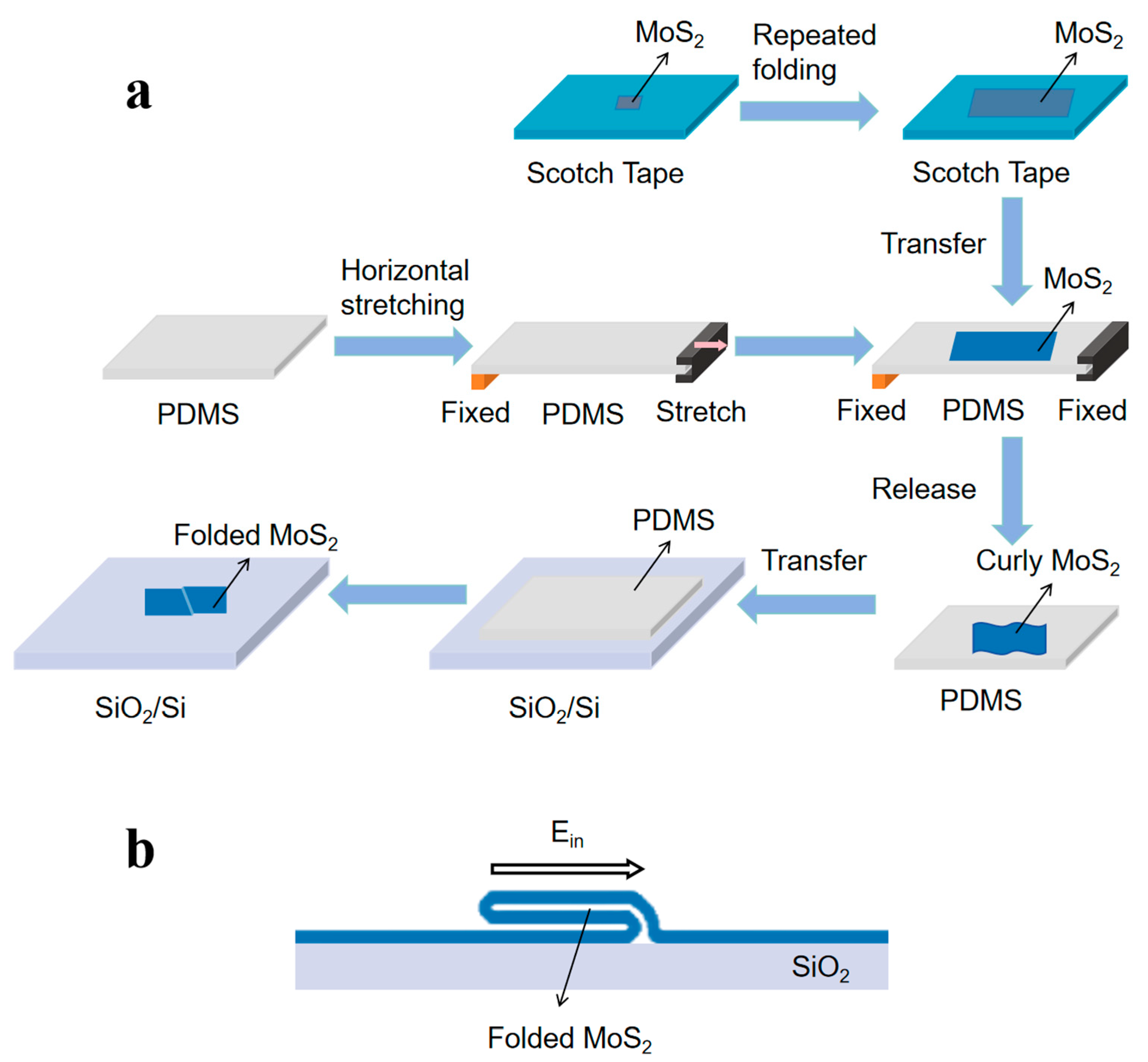
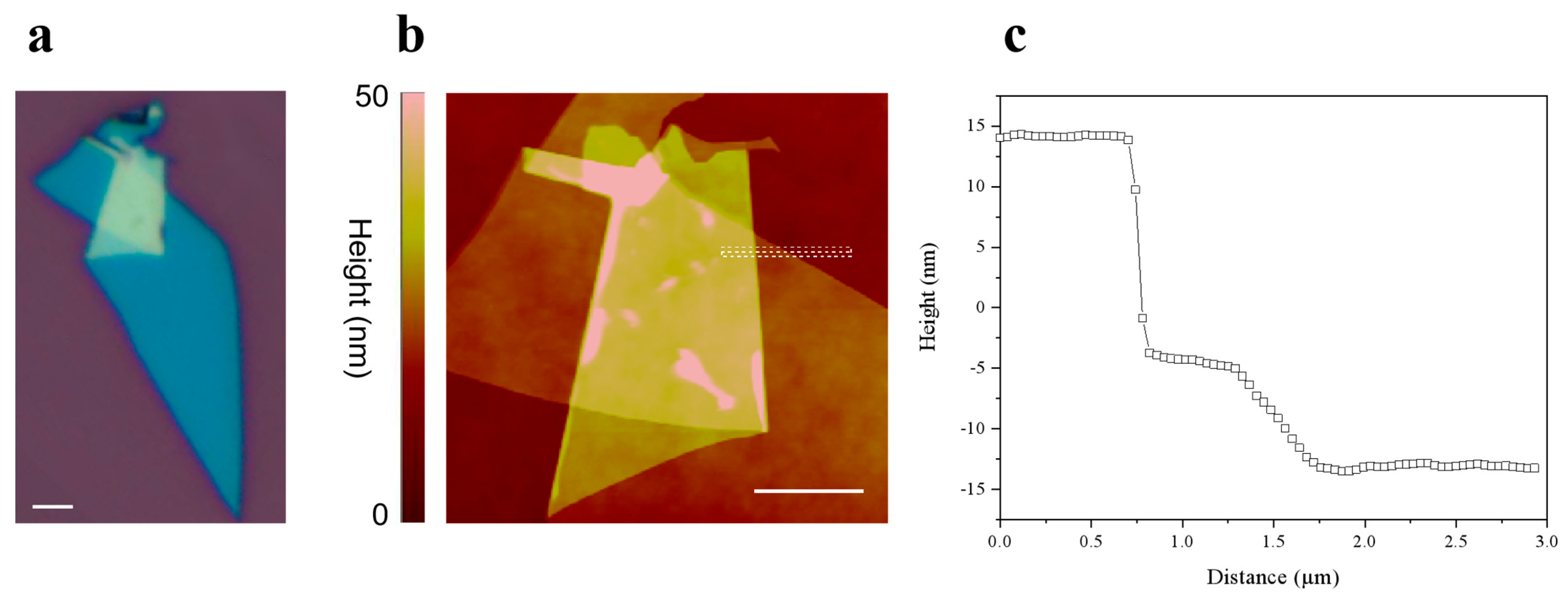
2. Methods
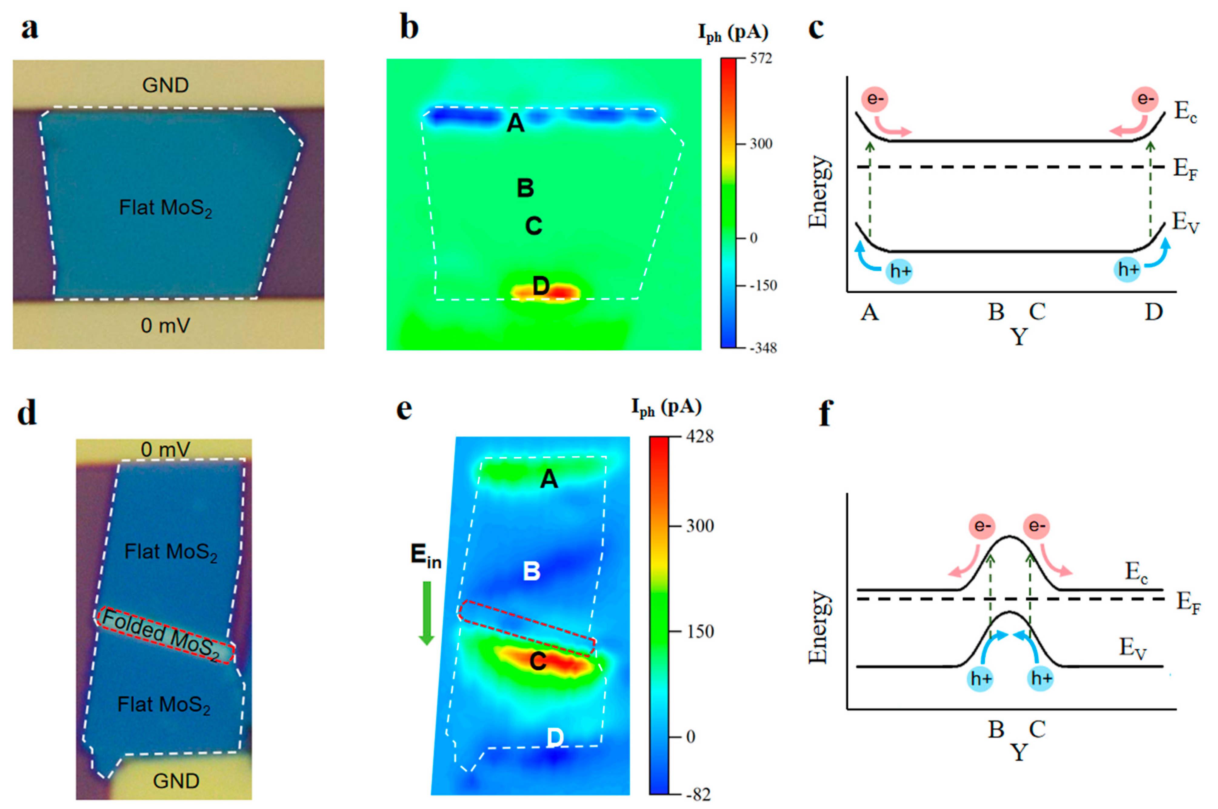
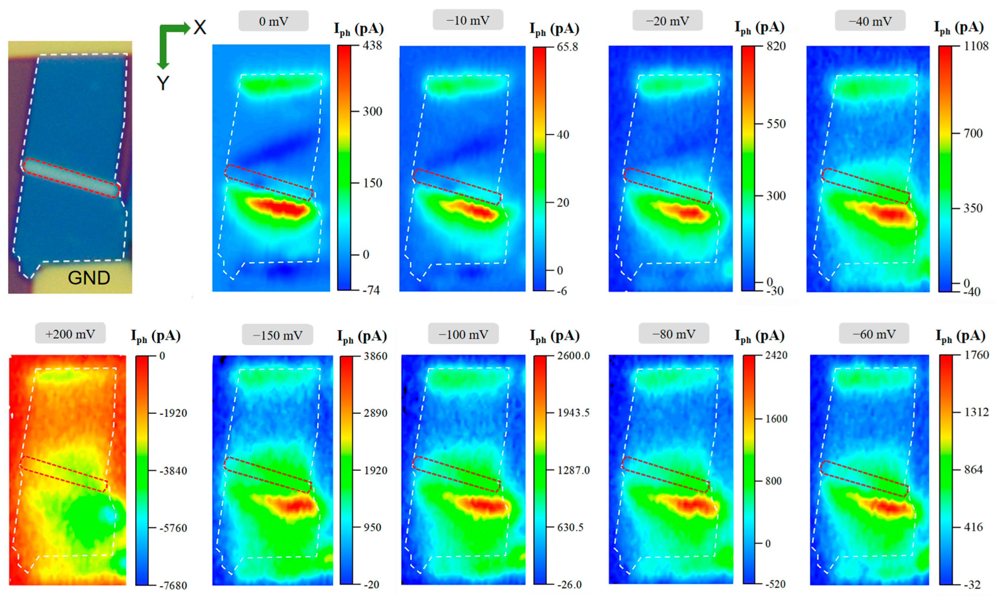
3. Results and Discussion
4. Conclusions
Author Contributions
Funding
Data Availability Statement
Conflicts of Interest
References
- Mak, K.F.; Lee, C.; Hone, J.; Shan, J.; Heinz, T.F. Atomically thin MoS2: A new direct-gap semiconductor. Phys. Rev. Lett. 2010, 105, 136805. [Google Scholar] [CrossRef] [PubMed]
- Wang, Q.H.; Kalantar-Zadeh, K.; Kis, A.; Coleman, J.N.; Strano, M.S. Electronics and optoelectronics of two-dimensional transition metal dichalcogenides. Nat. Nanotechnol. 2012, 7, 699–712. [Google Scholar] [CrossRef]
- Novoselov, K.S.; Geim, A.K.; Morozov, S.V.; Jiang, D.; Zhang, Y.; Dubonos, S.V.; Grigorieva, I.V.; Firsov, A.A. Electric Field Effect in Atomically Thin Carbon Films. Science 2004, 306, 666–669. [Google Scholar] [CrossRef]
- Kwon, J.; Seol, M.; Yoo, J.; Ryu, H.; Ko, D.S.; Lee, M.H.; Lee, E.K.; Yoo, M.S.; Lee, G.H.; Shin, H.J.; et al. 200-mm-wafer-scale integration of polycrystalline molybdenum disulfide transistors. Nat. Electron. 2024, 7, 356–364. [Google Scholar] [CrossRef]
- Hwangbo, S.; Hu, L.; Hoang, A.T.; Choi, J.Y.; Ahn, J.H. Wafer-scale monolithic integration of full-colour micro-LED display using MoS2 transistor. Nat. Nanotechnol. 2022, 17, 500–506. [Google Scholar] [CrossRef] [PubMed]
- Liu, L.T.; Kong, L.A.; Li, Q.Y.; He, C.L.; Ren, L.W.; Tao, Q.Y.; Yang, X.D.; Lin, J.; Zhao, B.; Li, Z.W.; et al. Transferred van der Waals metal electrodes for sub-1-nm MoS2 vertical transistors. Nat. Electron. 2021, 4, 342–347. [Google Scholar] [CrossRef]
- Coleman, J.N.; Lotya, M.; O’Neill, A.; Bergin, S.D.; King, P.J.; Khan, U.; Young, K.; Gaucher, A.; De, S.; Smith, R.J.; et al. Two-Dimensional Nanosheets Produced by Liquid Exfoliation of Layered Materials. Science 2011, 331, 568–571. [Google Scholar] [CrossRef]
- Manzeli, S.; Allain, A.; Ghadimi, A.; Kis, A. Piezoresistivity and Strain-induced Band Gap Tuning in Atomically Thin MoS2. Nano Lett. 2015, 15, 5330–5335. [Google Scholar] [CrossRef]
- Feng, G.; Liu, Y.; Zhu, Q.; Feng, Z.; Luo, S.; Qin, C.; Chen, L.; Xu, Y.; Wang, H.; Zubair, M.; et al. Giant tunnel electroresistance through a Van der Waals junction by external ferroelectric polarization. Nat. Commun. 2024, 15, 9701. [Google Scholar] [CrossRef]
- Zhao, Y.; Chen, F.; Liang, J.; Bahramy, M.S.; Yang, M.; Guang, Y.; Li, X.; Wei, Z.; Tang, J.; Zhao, J.; et al. Origin of Nonlinear Circular Photocurrent in 2D Semiconductor MoS_2. Phys. Rev. Lett. 2025, 134, 086201. [Google Scholar] [CrossRef]
- Wang, H.; Wang, F.; Xia, H.; Wang, P.; Li, T.; Li, J.; Wang, Z.; Sun, J.; Wu, P.; Ye, J.; et al. Direct observation and manipulation of hot electrons at room temperature. Natl. Sci. Rev. 2021, 8, nwaa295. [Google Scholar] [CrossRef] [PubMed]
- Wang, H.; Wang, F.; Xu, T.; Xia, H.; Xie, R.; Zhou, X.; Ge, X.; Liu, W.; Zhu, Y.; Sun, L.; et al. Slowing Hot-Electron Relaxation in Mix-Phase Nanowires for Hot-Carrier Photovoltaics. Nano Lett. 2021, 21, 7761–7768. [Google Scholar] [CrossRef] [PubMed]
- Nguyen, C.V.; Hieu, N.N.; Ilyasov, V.V. Band Gap Modulation of Bilayer MoS2 Under Strain Engineering and Electric Field: A Density Functional Theory. J. Electron. Mater. 2016, 45, 4038–4043. [Google Scholar] [CrossRef]
- Mei, J.; Zhang, Y.; Liao, T.; Sun, Z.; Dou, S.X. Strategies for improving the lithium-storage performance of 2D nanomaterials. Natl. Sci. Rev. 2018, 5, 389–416. [Google Scholar] [CrossRef]
- Wang, H.; Xia, H.; Liu, Y.; Chen, Y.; Xie, R.; Wang, Z.; Wang, P.; Miao, J.; Wang, F.; Li, T.; et al. Room-temperature low-threshold avalanche effect in stepwise van-der-Waals homojunction photodiodes. Nat. Commun. 2024, 15, 3639. [Google Scholar] [CrossRef]
- Zhou, H.; Auerbach, N.; Uzan, M.; Zhou, Y.; Banu, N.; Zhi, W.; Huber, M.E.; Watanabe, K.; Taniguchi, T.; Myasoedov, Y.; et al. Imaging quantum oscillations and millitesla pseudomagnetic fields in graphene. Nature 2023, 624, 275–281. [Google Scholar] [CrossRef] [PubMed]
- Wen, Z.; Ling, H.; Xin, W.; Zhou, T.; Wang, N.; Zhang, Y.; Xia, S.; Guo, J.; Tian, C.; Kong, X.Y.; et al. Engineered Band Alignment of Semiconductive Nanofluidics for Photo-Electro-Ion Mediated Ultrahigh Osmotic Energy Harvesting. Adv. Funct. Mater. 2025, 2425595. [Google Scholar] [CrossRef]
- Chen, X.; Feng, W.; Fang, Y.; Li, Q.; Huang, Y.H.; Chang, X.; Yao, C.; Shen, Y.; Liu, G.; Yang, S.; et al. Improved Conductivity of 2D Perovskite Capping Layer for Realizing High-Performance 3D/2D Heterostructured Hole Transport Layer-Free Perovskite Photovoltaics. Acs Nano 2025, 19, 4299–4308. [Google Scholar] [CrossRef] [PubMed]
- Meng, Y.-X.; Zhao, Y.-F.; Li, S.-C. Research progress of puckered honeycomb monolayers. Acta Phys. Sin. 2021, 70, 148101. [Google Scholar] [CrossRef]
- Xie, W.; Wei, Y. Roughening for Strengthening and Toughening in Monolayer Carbon Based Composites. Nano Lett. 2021, 21, 4823–4829. [Google Scholar] [CrossRef]
- Ren, K.; Shu, H.; Wang, K.; Qin, H. Two-dimensional MX(2)Y(4) systems: Ultrahigh carrier transport and excellent hydrogen evolution reaction performances. Phys. Chem. Chem. Phys. 2023, 25, 4519–4527. [Google Scholar] [CrossRef] [PubMed]
- Zhao, C.; Tian, W.; Sun, Q.; Yin, Z.; Leng, J.; Wang, S.; Liu, J.; Wu, K.; Jin, S. Trap-Enabled Long-Distance Carrier Transport in Perovskite Quantum Wells. J. Am. Chem. Soc. 2020, 142, 15091–15097. [Google Scholar] [CrossRef]
- Zhang, W.; Zhao, Z.; Yang, Y.; Zhang, Y.; Hao, H.; Li, L.; Xu, W.; Peng, B.; Long, R.; Liu, N. Paraffin-Enabled Compressive Folding of Two-Dimensional Materials with Controllable Broadening of the Electronic Band Gap. ACS Appl. Mater. Interfaces 2021, 13, 40922–40931. [Google Scholar] [CrossRef]
- Khan, A.R.; Lu, T.; Ma, W.; Lu, Y.; Liu, Y. Tunable Optoelectronic Properties of WS2 by Local Strain Engineering and Folding. Adv. Electron. Mater. 2020, 6, 1901381. [Google Scholar] [CrossRef]
- Amorim, B.; Cortijo, A.; de Juan, F.; Grushin, A.G.; Guinea, F.; Gutiérrez-Rubio, A.; Ochoa, H.; Parente, V.; Roldán, R.; San-Jose, P.; et al. Novel effects of strains in graphene and other two dimensional materials. Phys. Rep. 2016, 617, 1–54. [Google Scholar] [CrossRef]
- Li, Z.; Young, R.J.; Papageorgiou, D.G.; Kinloch, I.A.; Zhao, X.; Yang, C.; Hao, S. Interfacial stress transfer in strain engineered wrinkled and folded graphene. 2D Mater. 2019, 6, 4. [Google Scholar] [CrossRef]
- Rahman, S.; Yildirim, T.; Tebyetekerwa, M.; Khan, A.R.; Lu, Y. Extraordinary Nonlinear Optical Interaction from Strained Nanostructures in van der Waals CuInP(2)S(6). Acs Nano 2022, 16, 13959–13968. [Google Scholar] [CrossRef] [PubMed]
- Khan, A.R.; Liu, B.; Lu, T.; Zhang, L.; Sharma, A.; Zhu, Y.; Ma, W.; Lu, Y. Direct Measurement of Folding Angle and Strain Vector in Atomically Thin WS(2) Using Second-Harmonic Generation. Acs Nano 2020, 14, 15806–15815. [Google Scholar] [CrossRef]
- Becker, C.; Bao, B.; Karnaushenko, D.D.; Bandari, V.K.; Rivkin, B.; Li, Z.; Faghih, M.; Karnaushenko, D.; Schmidt, O.G. A new dimension for magnetosensitive e-skins: Active matrix integrated micro-origami sensor arrays. Nat. Commun. 2022, 13, 2121. [Google Scholar] [CrossRef]
- Lin, P.; Pan, C.; Wang, Z.L. Two-dimensional nanomaterials for novel piezotronics and piezophototronics. Mater. Today Nano 2018, 4, 17–31. [Google Scholar] [CrossRef]

Disclaimer/Publisher’s Note: The statements, opinions and data contained in all publications are solely those of the individual author(s) and contributor(s) and not of MDPI and/or the editor(s). MDPI and/or the editor(s) disclaim responsibility for any injury to people or property resulting from any ideas, methods, instructions or products referred to in the content. |
© 2025 by the authors. Licensee MDPI, Basel, Switzerland. This article is an open access article distributed under the terms and conditions of the Creative Commons Attribution (CC BY) license (https://creativecommons.org/licenses/by/4.0/).
Share and Cite
Zhang, B.; Liu, Y.; Chen, Z.; Wang, X. Deformation-Tailored MoS2 Optoelectronics: Fold-Induced Band Reconstruction for Programmable Polarity Switching. Nanomaterials 2025, 15, 727. https://doi.org/10.3390/nano15100727
Zhang B, Liu Y, Chen Z, Wang X. Deformation-Tailored MoS2 Optoelectronics: Fold-Induced Band Reconstruction for Programmable Polarity Switching. Nanomaterials. 2025; 15(10):727. https://doi.org/10.3390/nano15100727
Chicago/Turabian StyleZhang, Bo, Yaqian Liu, Zhen Chen, and Xiaofang Wang. 2025. "Deformation-Tailored MoS2 Optoelectronics: Fold-Induced Band Reconstruction for Programmable Polarity Switching" Nanomaterials 15, no. 10: 727. https://doi.org/10.3390/nano15100727
APA StyleZhang, B., Liu, Y., Chen, Z., & Wang, X. (2025). Deformation-Tailored MoS2 Optoelectronics: Fold-Induced Band Reconstruction for Programmable Polarity Switching. Nanomaterials, 15(10), 727. https://doi.org/10.3390/nano15100727