
High-Contrast and High-Speed Optical Logic Operations Using Silicon Microring Resonators


Abstract
1. Introduction
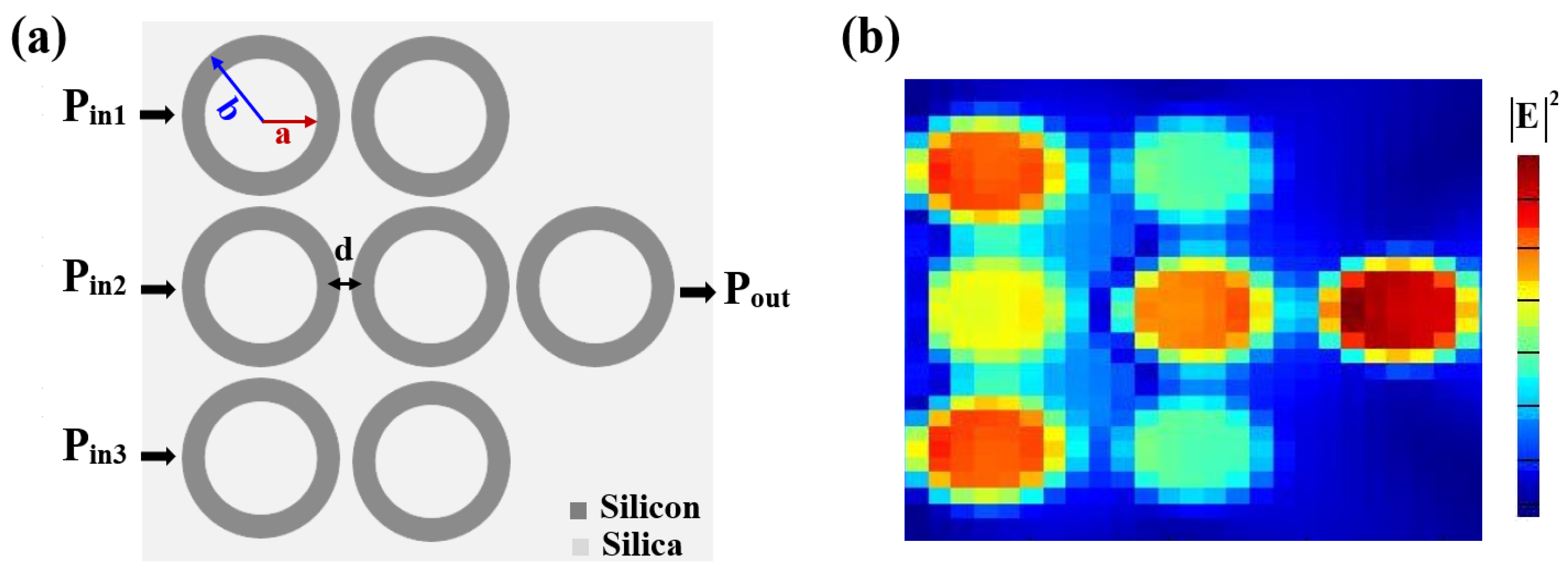
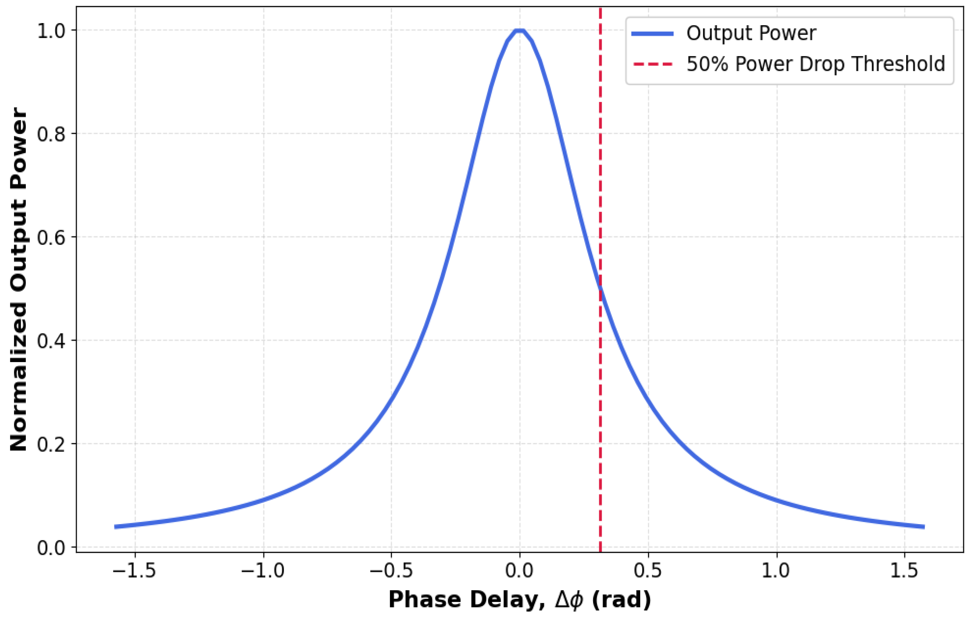
2. Waveguide Design
3. Optical Logic Operations
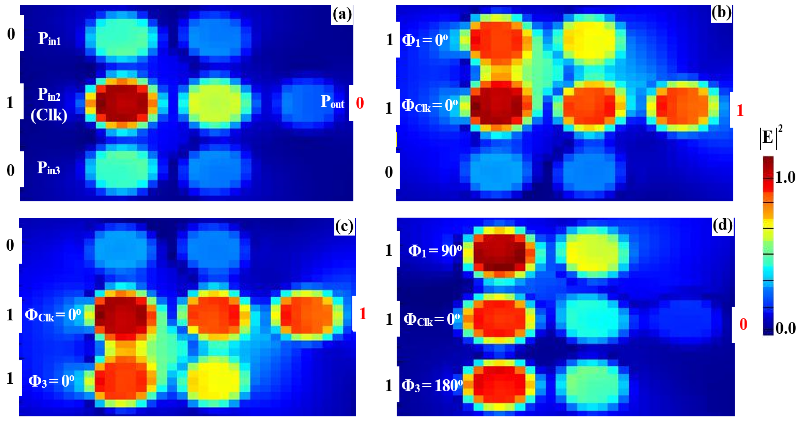
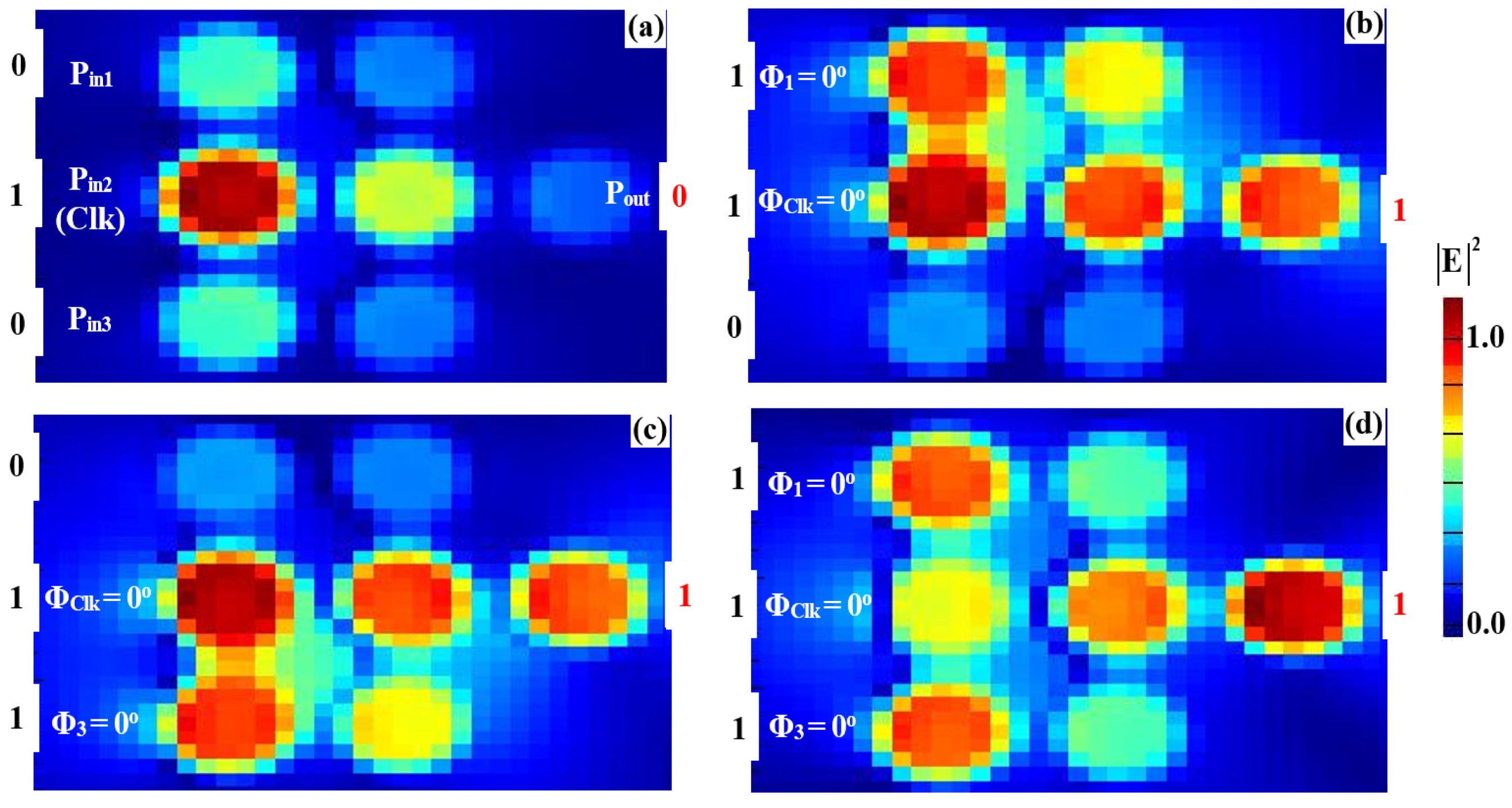
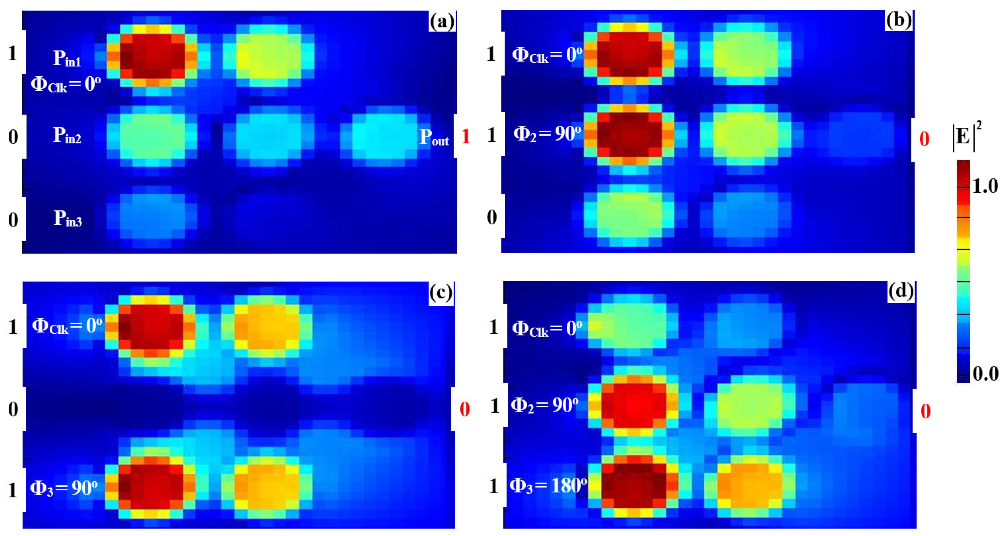
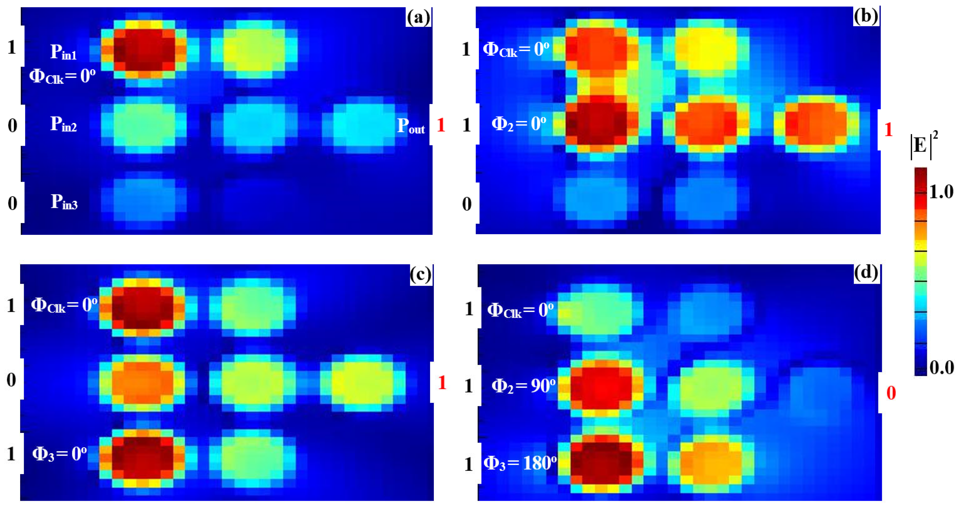
3.1. XOR, AND, OR
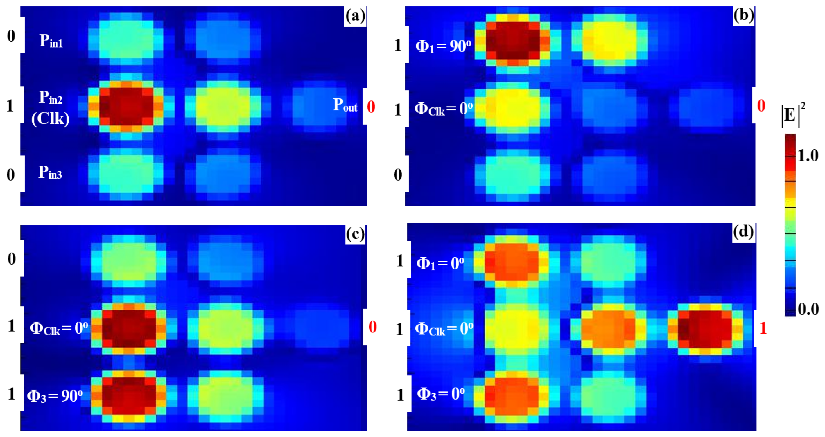
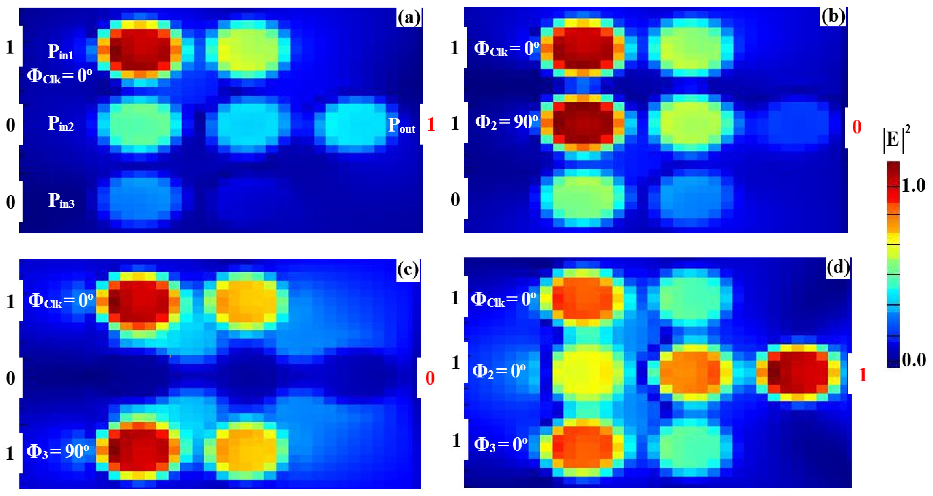
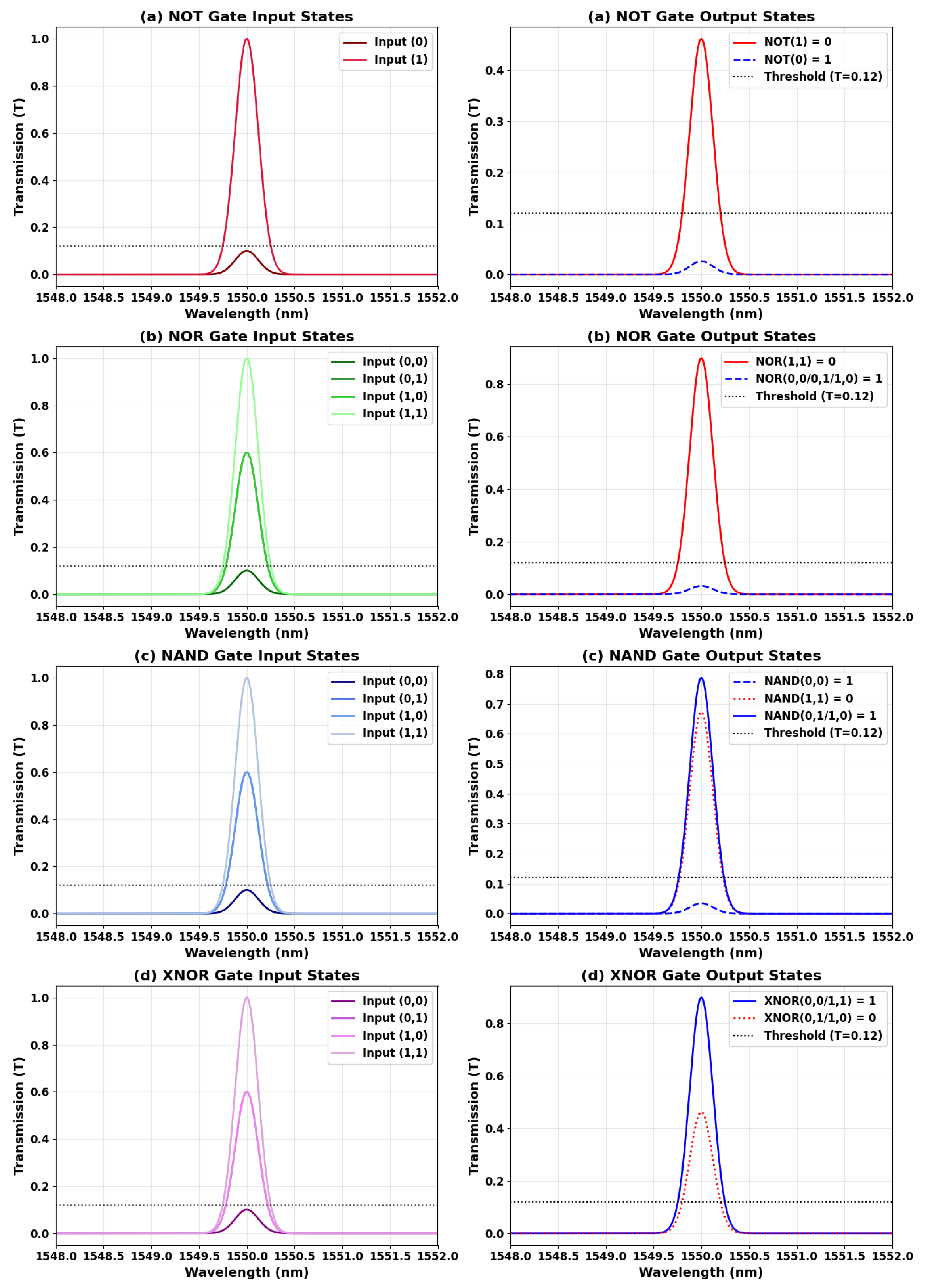
3.2. NOT, NOR, NAND, and XNOR
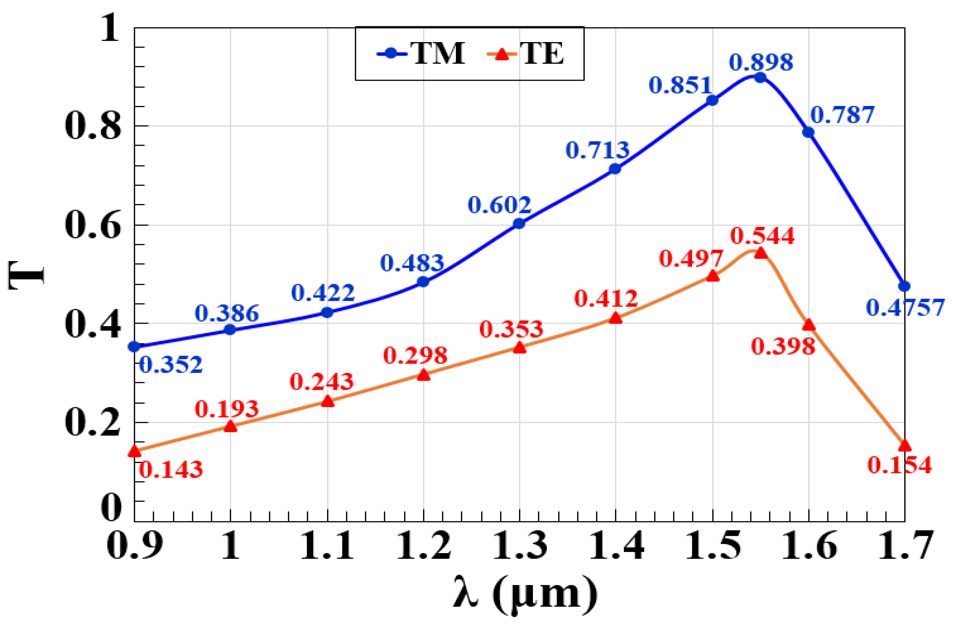
4. Performance Comparison
5. Data Rate Performance
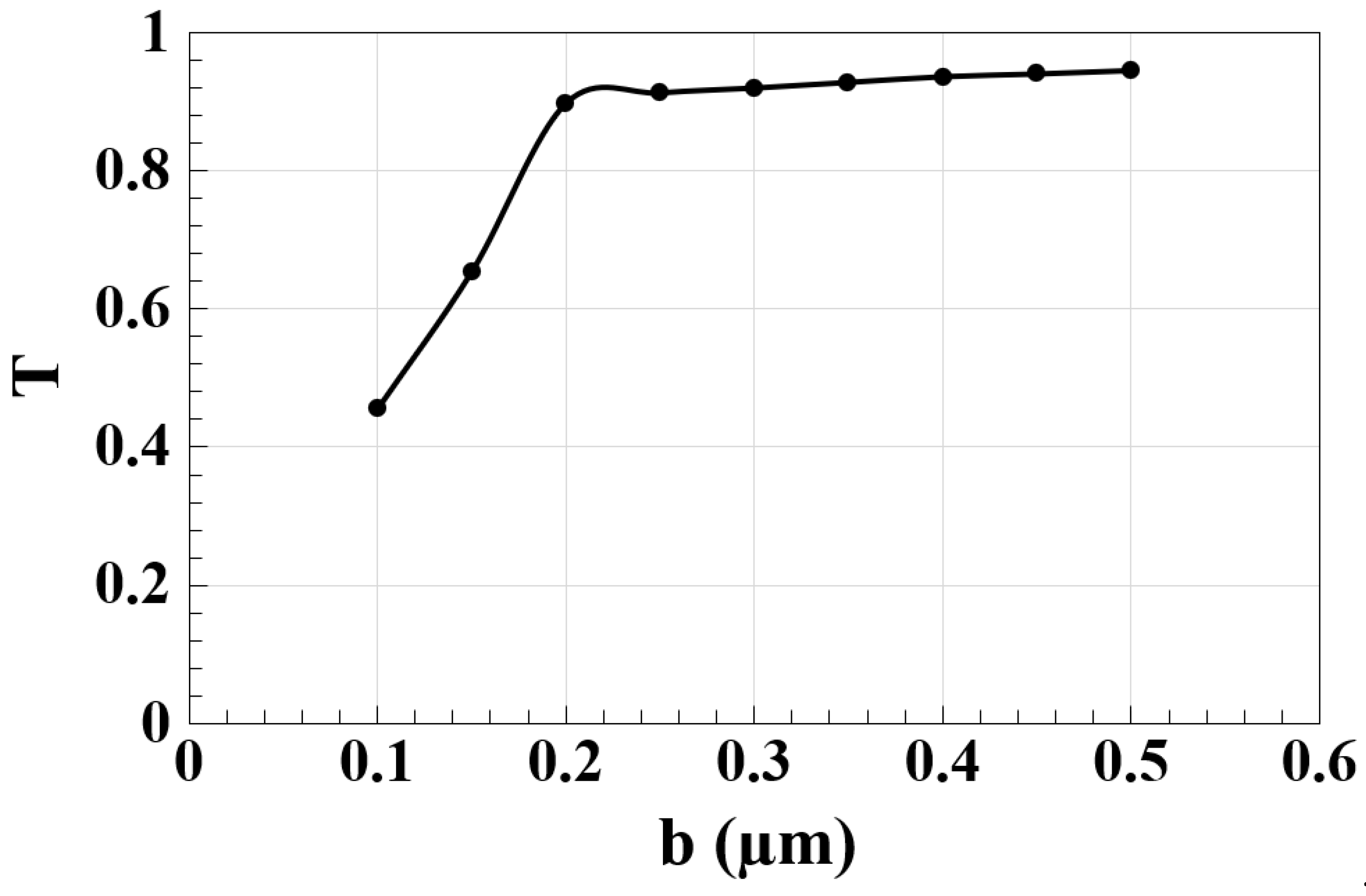
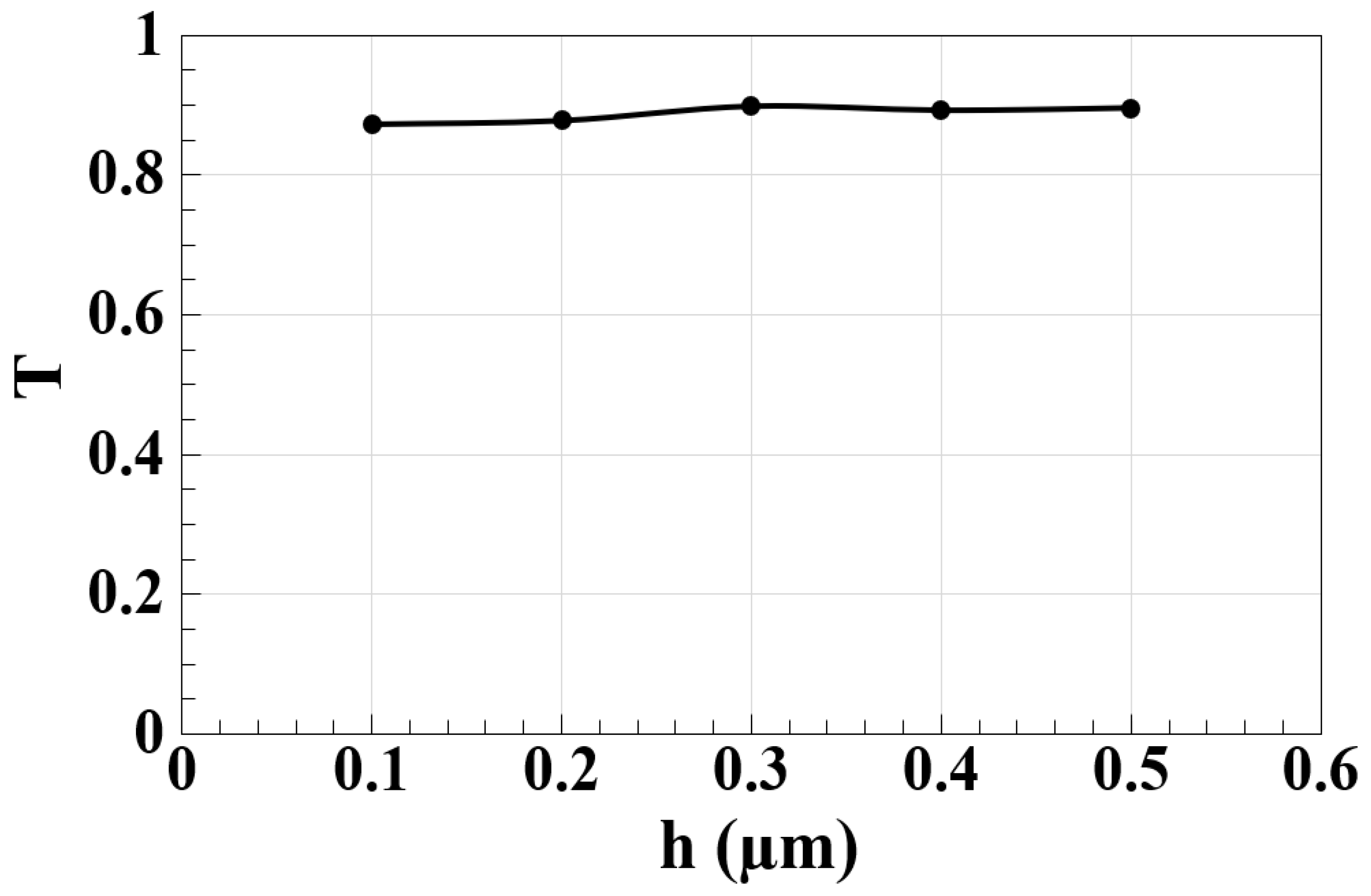
6. Fabrication Feasibility and Performance Characteristics
7. Conclusions
Author Contributions
Funding
Data Availability Statement
Acknowledgments
Conflicts of Interest
References
- Mirza, A.; Sunny, F.; Walsh, P.; Hassan, K.; Pasricha, S.; Nikdast, M. Silicon Photonic Microring Resonators: A Comprehensive Design-Space Exploration and Optimization Under Fabrication-Process Variations. IEEE Trans. Comput. Aided Des. Integr. Circuits Syst. 2022, 41, 3359–3372. [Google Scholar] [CrossRef]
- Donzella, V.; Sherwali, A.; Flueckiger, J.; Grist, S.M.; Talebi Fard, S.; Chrostowski, L. Design and fabrication of SOI micro-ring resonators based on sub-wavelength grating waveguides. Opt. Express 2015, 23, 4791–4803. [Google Scholar] [CrossRef]
- Bogaerts, W.; Heyn, P.D.; Vaerenbergh, T.V.; Vos, K.D.; Selvaraja, S.K.; Claes, T.; Dumon, P.; Bienstman, P.; Thourhout, D.V.; Baets, R. Silicon microring resonators. Laser Photon. Rev. 2012, 6, 47–73. [Google Scholar] [CrossRef]
- Lipson, M. The revolution of silicon photonics. Nat. Mater. 2022, 21, 974–975. [Google Scholar] [CrossRef]
- Dai, D.; Liang, D.; Cheben, P. Next-generation silicon photonics: Introduction. Photon. Res. 2022, 10, NGSP1–NGSP3. [Google Scholar] [CrossRef]
- Baets, R.; Van Thourhout, D.; Bienstman, P.; Roelkens, G.; Dumon, P.; Bogaerts, W. Silicon Photonics: Opportunities and Challenges. In Asia Optical Fiber Communication and Optoelectronic Exposition and Conference; OSA Technical Digest (CD); Optica Publishing Group: Washington, DC, USA, 2008; paper SaH1. [Google Scholar]
- Jalali, B.; Fathpour, S. Silicon photonics. J. Lightwave Technol. 2006, 24, 4600–4615. [Google Scholar] [CrossRef]
- Stojanović, V.; Ram, R.J.; Popović, M.; Lin, S.; Moazeni, S.; Wade, M.; Sun, C.; Alloatti, L.; Atabaki, A.; Pavanello, F.; et al. Monolithic silicon-photonic platforms in state-of-the-art CMOS SOI processes. Opt. Express 2018, 26, 13106–13121. [Google Scholar] [CrossRef]
- Kotb, A.; Zoiros, K.E.; Li, W. Silicon-on-silica waveguides-based all-optical logic gates. Phys. Scr. 2023, 98, 035517. [Google Scholar] [CrossRef]
- Kotb, A.; Yao, C. All-optical logic operations based on silicon-on-insulator waveguides. Opt. Eng. 2023, 62, 048101. [Google Scholar] [CrossRef]
- Kita, S.; Nozaki, K.; Takata, K.; Shinya, A.; Notomi, M. Ultrashort low-loss Ψ gates for linear optical logic on Si photonics platform. Commun. Phys. 2020, 3, 33. [Google Scholar] [CrossRef]
- Han, H.L.; Li, H.; Zhang, X.P.; Liu, A.; Lin, T.Y.; Chen, Z.; Lv, H.B.; Lu, M.H.; Liu, X.P.; Chen, Y.F. High performance ultra-compact SOI waveguide crossing. Opt. Express 2018, 26, 25602–25610. [Google Scholar] [CrossRef]
- Zhang, Y.; Ling, Y.-C.; Zhang, Y.; Shang, K.; Yoo, S.J.B. High-Density Wafer-Scale 3-D Silicon-Photonic Integrated Circuits. IEEE J. Sel. Top. Quantum Electron. 2018, 24, 8200510. [Google Scholar] [CrossRef]
- Ishizaka, Y.; Kawaguchi, Y.; Saitoh, K.; Koshiba, M. Design of ultracompact all-optical XOR and AND logic gates with low power consumption. Opt. Commun. 2011, 284, 3528–3533. [Google Scholar] [CrossRef]
- Husko, C.; Vo, T.D.; Corcoran, B.; Li, J.; Krauss, T.; Eggleton, B. Ultracompact all-optical XOR logic gate in a slow-light silicon photonic crystal waveguide. Opt. Express 2011, 19, 20681–20690. [Google Scholar] [CrossRef]
- Xu, Q.; Lipson, M. All-optical logic based on silicon micro-ring resonators. Opt. Express 2007, 15, 924–929. [Google Scholar] [CrossRef]
- Almeida, V.R.; Barrios, C.A.; Panepucci, R.R.; Lipson, M.; Foster, M.A.; Ouzounov, D.G.; Gaeta, A.L. All-optical switching on a silicon chip. Opt. Lett. 2004, 29, 2867–2869. [Google Scholar] [CrossRef]
- Law, F.K.; Uddin, M.R.; Hashim, H.; Hamid, Z. Simulation and Demonstration of Electro-Optic Digital Logic Gates Based on a Single Microring Resonator. Opt. Quant. Electron. 2017, 49, 413. [Google Scholar] [CrossRef]
- Law, F.K.; Uddin, M.R. Digital Electro-Optic Exclusive OR and NOR Gates Utilizing a Single Micro-Ring Resonator. Optik 2020, 200, 16336. [Google Scholar] [CrossRef]
- Law, F.K.; Uddin, M.R.; Hashim, H.; Won, Y.H. Demonstration of Photonic Micro-Ring Resonator Based Digital Bit Magnitude Comparator. Opt. Quant. Electron. 2019, 51, 1. [Google Scholar] [CrossRef]
- Law, F.K.; Uddin, M.R.; Hashim, H. Photonic D-Type Flip Flop Based on Micro-Ring Resonator. Opt. Quant. Electron. 2018, 50, 119. [Google Scholar] [CrossRef]
- Rani, P.; Kalra, Y.; Sinha, R.K. Design of all-optical logic gates in photonic crystal waveguides. Optik 2015, 126, 950–955. [Google Scholar] [CrossRef]
- Priya, N.H.; Swarnakar, S.; Krishna, S.V.; Kumar, S. Design and analysis of an optical three-input AND gate using a photonic crystal fiber. Appl. Opt. 2022, 61, 77–83. [Google Scholar]
- Priya, N.H.; Swarnakar, S.; Krishna, S.V.; Kumar, S. Design and analysis of a photonic crystal-based all-optical 3-input OR gate for high-speed optical processing. Opt. Quantum Electron. 2021, 53, 720. [Google Scholar] [CrossRef]
- Rao, D.G.S.; Swarnakar, S.; Palacharla, V.; Raju, K.S.R.; Kumar, S. Design of all-optical AND, OR, and XOR logic gates using photonic crystals for switching applications. Photon. Netw. Commun. 2021, 41, 109–118. [Google Scholar] [CrossRef]
- Mostafa, T.S.; Mohammed, N.A.; El-Rabaie, E.M. Ultra-high bit rate all-optical AND/OR logic gates based on photonic crystal with multi-wavelength simultaneous operation. J. Mod. Opt. 2019, 66, 1005–1016. [Google Scholar] [CrossRef]
- Pan, D.; Wei, H.; Xu, H. Optical interferometric logic gates based on metal slot waveguide network realizing whole fundamental logic operations. Opt. Express 2013, 21, 9556. [Google Scholar] [CrossRef]
- Bian, Y.; Gong, Q. Compact all-optical interferometric logic gates based on one-dimensional metal-insulator-metal structures. Opt. Commun. 2014, 313, 27–35. [Google Scholar] [CrossRef]
- Alali, M.J.; Raheema, M.N.; Alwahib, A.A. Nanoscale plasmonic logic gates design by using an elliptical resonator. Appl. Opt. 2023, 62, 4080–4088. [Google Scholar] [CrossRef]
- Neseli, B.; Yilmaz, Y.A.; Kurt, H.; Turduev, M. Inverse design of ultra-compact photonic gates for all-optical logic operations. J. Phys. D Appl. Phys. 2022, 55, 215107. [Google Scholar] [CrossRef]
- Webster, M.A.; Pafchek, R.M.; Mitchell, A.; Koch, T.L. Width Dependence of Inherent TM-Mode Lateral Leakage Loss in Silicon-On-Insulator Ridge Waveguides. IEEE Photonics Technol. Lett. 2007, 19, 429–431. [Google Scholar] [CrossRef]
- Fujie, A.; Shoji, Y.; Mizumoto, T. Silicon waveguide optical isolator integrated with TE-TM mode converter. In 2015 Optical Fiber Communications Conference and Exhibition (OFC); Optica Publishing Group: Los Angeles, CA, USA, 2015; pp. 1–3. [Google Scholar]
- Taflove, A.; Hagness, S.C. Computational Electrodynamics: The Finite-Difference Time-Domain Method, 3rd ed.; Artech House: Norwood, MA, USA, 2005. [Google Scholar]
- Liu, Y.; Zhang, W. Optimized Mesh Refinement for FDTD Simulations of Plasmonic Waveguides. J. Comput. Theor. Nanosci. 2017, 14, 3872–3877. [Google Scholar]
- Rahim, A.; Spuesens, T.; Baets, R.; Bogaerts, W. Open-access silicon photonics: Current status and emerging initiatives. Proc. IEEE 2013, 101, 214–231. [Google Scholar] [CrossRef]
- Poon, J.K.S.; Scheuer, J.; Xu, Y.; Yariv, A. Designing coupled-resonator optical waveguide delay lines. J. Opt. Soc. Am. B 2004, 21, 1665–1673. [Google Scholar] [CrossRef]
- Chen, L.; Preston, K.; Manipatruni, S. Reconfigurable Photonic Logic with On-Chip Pump Control. Optica 2022, 9, 128–135. [Google Scholar]
- Zhang, Y.; Li, X.; Chen, S. Time-Multiplexed Nonlinear Photonic Logic for Programmable Systems. Nat. Photon. 2021, 15, 442–448. [Google Scholar]
- Crisp, J.; Elliott, B. Introduction to Fiber Optics, 3rd ed.; Elsevier: Amsterdam, The Netherlands, 2005. [Google Scholar]
- Yang, J.; Wang, H.; Lu, L.; Liang, H.; Chen, Y. Ultra-Compact Silicon Photonic Devices Enabled by Advanced Lithography. Nat. Photon. 2020, 14, 595–602. [Google Scholar]
- Zhang, Y.; Li, X.; Chen, S.; Wang, P.; Liu, J. Sub-100 nm Silicon Photonic Devices via DUV Immersion Lithography. Optica 2020, 7, 218–224. [Google Scholar]
- Zhao, X.; Wu, P.; Liu, F. Wafer-scale silicon microfabrication technology toward realization of low-cost sub-THz waveguide devices. J. Micromech. Microeng. 2024, 34, 045003. [Google Scholar] [CrossRef]
- Lee, B.T.-H.; Huang, C.-H.; Ho, C.-C.; Lo, F.-S. Rapid Fabrication of 100 nm or Thinner Fully Depleted Silicon-on-Insulator Materials for Ultralow Energy Consumption. ACS Appl. Nano Mater. 2018, 1, 2414–2420. [Google Scholar] [CrossRef]
- Yang, J.; Wang, T.; Liu, Y. Sub-10 nm fabrication: Methods and applications. Nanotechnology 2021, 32, 412001. [Google Scholar]
- Eissa, M.; Mitarai, T.; Amemiya, T.; Miyamoto, Y.; Nishiyama, N. Fabrication of Si photonic waveguides by electron beam lithography using improved proximity effect correction. Jpn. J. Appl. Phys. 2020, 59, 126502. [Google Scholar] [CrossRef]
- Vlasov, Y.A.; McNab, S.J. Modal Engineering in Ultra-Compact Photonic Cavities. Opt. Express 2004, 12, 1622–1631. [Google Scholar] [CrossRef] [PubMed]
- Sun, C.; Wade, M.T.; Lee, Y. High-Density Optical Interconnects Using Subwavelength Resonators. Science 2021, 373, 95–98. [Google Scholar]
- Oulton, R.F.; Sorger, V.J.; Zentgraf, T. Hybrid Plasmonic Nanocavities for Enhanced Light-Matter Interaction. Nature 2009, 461, 629–632. [Google Scholar] [CrossRef]
- Chen, L.; Preston, K.; Manipatruni, S. Optimized Racetrack Resonators for CMOS Photonics. Opt. Lett. 2018, 43, 2208–2211. [Google Scholar]
- Piggott, A.Y.; Lu, J.; Lagoudakis, K.G. Inverse-Designed Photonic Components for Ultra-Compact Systems. Nat. Photon. 2017, 11, 374–379. [Google Scholar]
- De Vos, K.; Bartolozzi, I.; Schacht, E. Silicon-on-Insulator Microring Resonator for Sensitive Biomolecular Detection. Opt. Express 2007, 15, 7610–7615. [Google Scholar] [CrossRef]
- Padmaraju, K.; Bergman, K. Resolving the Energy Challenges of Optical Interconnects. IEEE J. Sel. Top. Quantum Electron. 2014, 20, 8200212. [Google Scholar]


| Mesh Size (nm) | Transmission | Loss (%) | Relative Cost * |
|---|---|---|---|
| 5 | 0.8934 | 10.66 | ~50× |
| 10 | 0.8936 | 10.64 | ~25× |
| 20 | 0.8951 | 10.49 | ~10× |
| 30 | 0.8911 | 10.89 | ~5× |
| 40 | 0.8940 | 10.60 | ~2× |
| 50 | 0.8980 | 10.20 | ~1× |
| Logic Operation | Input Signals | Output Logic | Pout (mW) | T | CR (dB) | ||
|---|---|---|---|---|---|---|---|
| Pin1 | Pin2 (Clk) | Pin3 | Pout | ||||
| XOR | 0 | 1 | 0 | 0 | 0.0074 | 0.031 | 14.04 |
| 1 | 1 | 0 | 1 | 0.1886 | 0.786 | ||
| 0 | 1 | 1 | 1 | 0.1886 | 0.786 | ||
| 1 | 1 | 1 | 0 | 0.0074 | 0.031 | ||
| AND | 0 | 1 | 0 | 0 | 0.0074 | 0.031 | 15.14 |
| 1 | 1 | 0 | 0 | 0.0069 | 0.029 | ||
| 0 | 1 | 1 | 0 | 0.0062 | 0.026 | ||
| 1 | 1 | 1 | 1 | 0.2155 | 0.898 | ||
| OR | 0 | 1 | 0 | 0 | 0.0074 | 0.031 | 15.85 |
| 1 | 1 | 0 | 1 | 0.1886 | 0.786 | ||
| 0 | 1 | 1 | 1 | 0.1886 | 0.786 | ||
| 1 | 1 | 1 | 1 | 0.2155 | 0.898 | ||
| Logic Operation | Input Signals | Output Logic | Pout (mW) | T | CR (dB) | ||
|---|---|---|---|---|---|---|---|
| Pin1 (CLK) | Pin2 | Pin3 | Pout | ||||
| NOT | 1 | - | 0 | 1 | 0.1109 | 0.462 | 13.42 |
| 1 | - | 1 | 0 | 0.0050 | 0.021 | ||
| NOR | 1 | 0 | 0 | 1 | 0.1109 | 0.462 | 12.02 |
| 1 | 1 | 0 | 0 | 0.0077 | 0.032 | ||
| 1 | 0 | 1 | 0 | 0.0050 | 0.021 | ||
| 1 | 1 | 1 | 0 | 0.0082 | 0.034 | ||
| NAND | 1 | 0 | 0 | 1 | 0.1109 | 0.462 | 12.75 |
| 1 | 1 | 0 | 1 | 0.1886 | 0.786 | ||
| 1 | 0 | 1 | 1 | 0.1613 | 0.672 | ||
| 1 | 1 | 1 | 0 | 0.0082 | 0.034 | ||
| XNOR | 1 | 0 | 0 | 0 | 0.1109 | 0.462 | 14.10 |
| 1 | 1 | 0 | 0 | 0.0077 | 0.032 | ||
| 1 | 0 | 1 | 0 | 0.0050 | 0.021 | ||
| 1 | 1 | 1 | 1 | 0.2155 | 0.898 | ||
| Logic Operations | Waveguide | Materials | Size (μm2) | λ (nm) | Metric (dB) | Experimental/ Simulation | Ref. |
|---|---|---|---|---|---|---|---|
| AND, NOR, XNOR | Si photonics platform | Si | ~3 μm-long | 1550 | CR > 10 | Exp. | [11] |
| AND, NAND | Silicon micro-ring resonators | Si/SiO2 | 0.45 × 0.25 | 1550.7 | ER~10 | Exp. | [16] |
| AND, XOR, OR, NOT, NAND, NOR XNOR | PhC waveguides | Si/Air | 9 × 5 | 1550 | CR = 5.42–9.59 | Sim. | [22] |
| AND, XOR, XNOR | T-shaped PhC waveguides | Si/Air | - | 1550 | CR = 8.29–33.05 | Sim. | [23,24,25] |
| AND, OR | 2D PhC design | Si /Air | 19.8 × 12.6 | 1520 | CR = 9.74 and 17.95 | Sim. | [26] |
| NOT, XOR, AND, OR, NOR, NAND, XNOR | Metal slot waveguide | Silver/SiO2 | 1.5 × 2.36 | 632.8 | CR = 6–16 | Exp. | [27] |
| NOT, XOR, AND, OR, NOR, NAND, XNOR | Metal–insulator–metal structures | Air/Silver | 5.33 × 0.42 | 632.8 | CR = 15 | Sim. | [28] |
| AND, NAND, OR, XOR, NOR, XNAOR, NOT | Plasmonic logic gates design | Silver/SiO2 | 0.25 × 0.25 | 850 | CR = 4.14–14.46 | Sim. | [29] |
| AND, OR, NOT, NAND | Inverse design on silicon platforms | Si/SiO2 | 1.0 × 1.5 | 1300 | CR = 0.5–5.79 | Sim. | [30] |
| XOR, AND, OR, NOT, NOR, XNOR, NAND | Silicon microrings waveguide | Si/SiO2 | 1.30 × 1.35 | 1550 | CR = 12.02–15.85 | Sim. | This work |
Disclaimer/Publisher’s Note: The statements, opinions and data contained in all publications are solely those of the individual author(s) and contributor(s) and not of MDPI and/or the editor(s). MDPI and/or the editor(s) disclaim responsibility for any injury to people or property resulting from any ideas, methods, instructions or products referred to in the content. |
© 2025 by the authors. Licensee MDPI, Basel, Switzerland. This article is an open access article distributed under the terms and conditions of the Creative Commons Attribution (CC BY) license (https://creativecommons.org/licenses/by/4.0/).
Share and Cite
Kotb, A.; Wang, Z.; Chen, W. High-Contrast and High-Speed Optical Logic Operations Using Silicon Microring Resonators. Nanomaterials 2025, 15, 707. https://doi.org/10.3390/nano15100707
Kotb A, Wang Z, Chen W. High-Contrast and High-Speed Optical Logic Operations Using Silicon Microring Resonators. Nanomaterials. 2025; 15(10):707. https://doi.org/10.3390/nano15100707
Chicago/Turabian StyleKotb, Amer, Zhiyang Wang, and Wei Chen. 2025. "High-Contrast and High-Speed Optical Logic Operations Using Silicon Microring Resonators" Nanomaterials 15, no. 10: 707. https://doi.org/10.3390/nano15100707
APA StyleKotb, A., Wang, Z., & Chen, W. (2025). High-Contrast and High-Speed Optical Logic Operations Using Silicon Microring Resonators. Nanomaterials, 15(10), 707. https://doi.org/10.3390/nano15100707