


Multi-Layer Palladium Diselenide as a Contact Material for Two-Dimensional Tungsten Diselenide Field-Effect Transistors
 , , , , , , , and
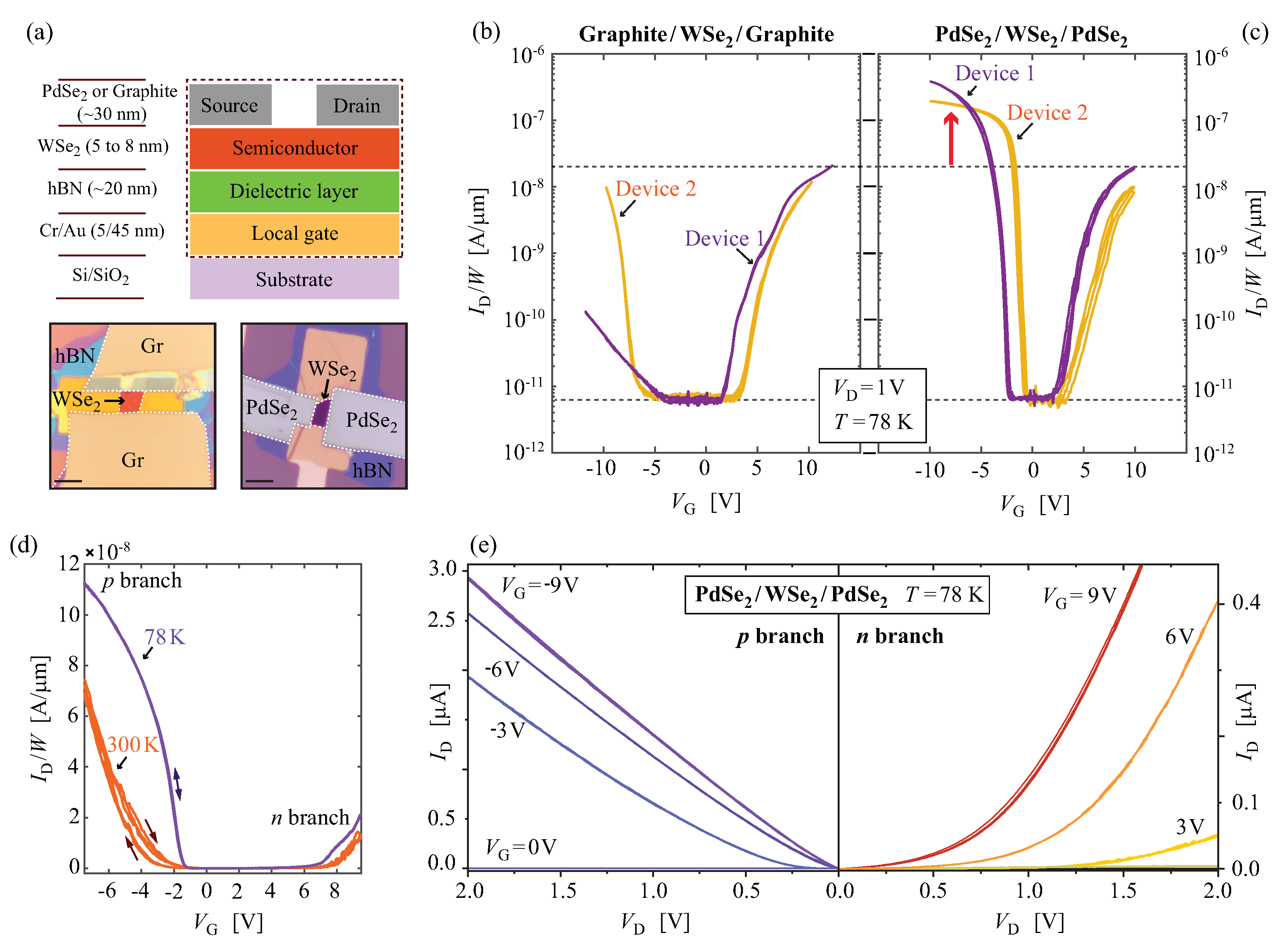
Abstract
1. Introduction
2. Materials and Methods
2.1. Crystal Growth
2.2. Device Fabrication
2.3. Electrical Characterization
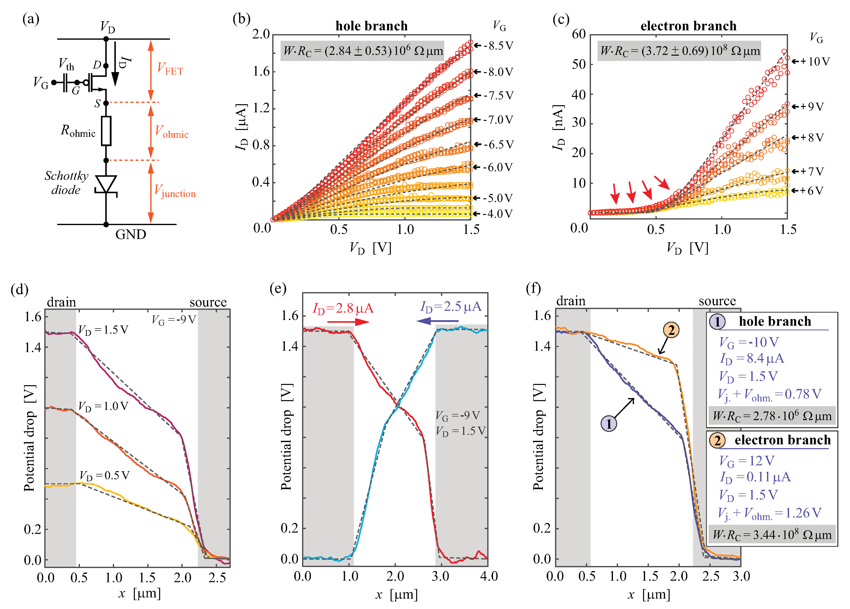
2.4. FET Figures of Merit (FOM) Extraction and Device Modelling
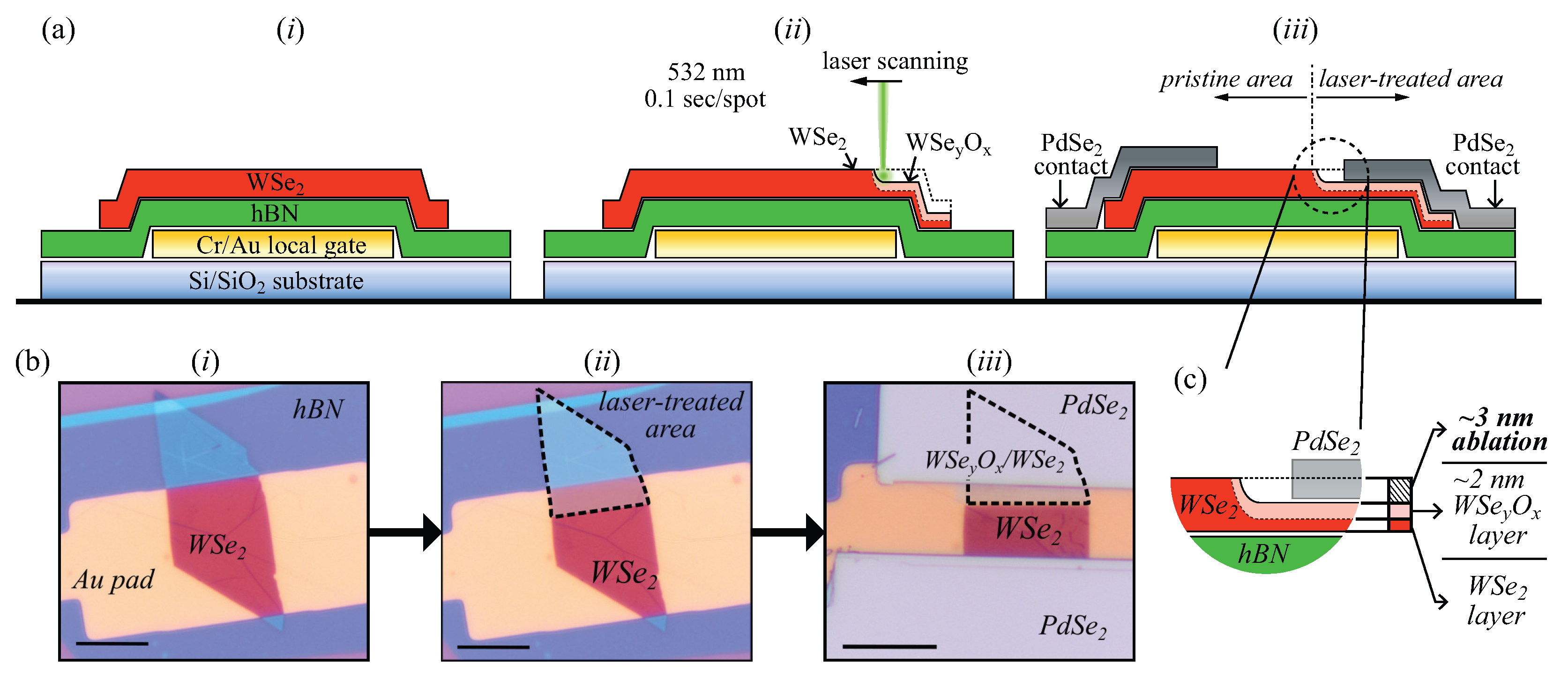
2.5. Laser Treatment of
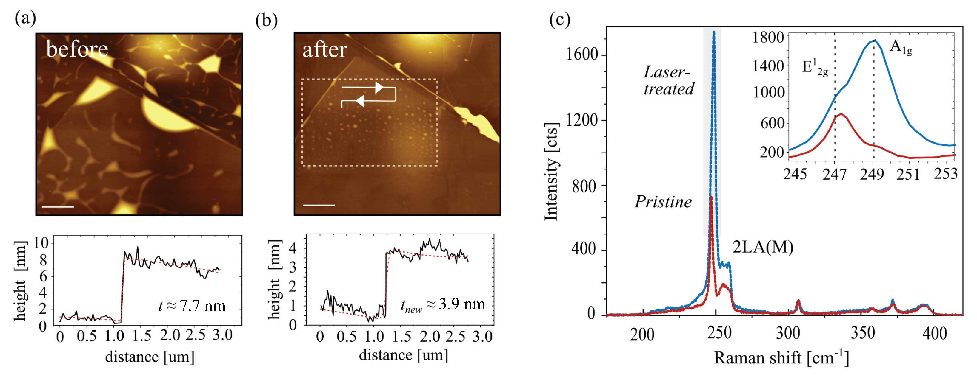
2.6. AFM and In Operando KPFM Measurements
2.7. Raman Spectroscopy
3. Results and Discussions
3.1. Electrical Characteristics of FETs with Graphite and Electrodes
3.2. Contact Resistance of the Interface
3.3. Optimizing Contact Interface via Laser-Driven Oxidation of
3.4. Electrical Characteristics of FETs with Electrode Interface
4. Conclusions
Author Contributions
Funding
Data Availability Statement
Conflicts of Interest
References
- Cao, W.; Bu, H.; Vinet, M.; Cao, M.; Takagi, S.; Hwang, S.; Ghani, T.; Banerjee, K. The future transistors. Nature 2023, 620, 501–515. [Google Scholar] [CrossRef]
- Zhu, K.; Wen, C.; Aljarb, A.A.; Xue, F.; Xu, X.; Tung, V.; Zhang, X.; Alshareef, H.N.; Lanza, M. The development of integrated circuits based on two-dimensional materials. Nat. Electron. 2021, 11, 775–785. [Google Scholar] [CrossRef]
- Ahmad, W.; Gong, Y.; Abbas, G.; Khan, K.; Khan, M.; Ali, G.; Shuja, A.; Tareen, A.K.; Khan, Q.; Li, D. Evolution of low-dimensional material-based field-effect transistors. Nanoscale 2021, 10, 5162–5186. [Google Scholar] [CrossRef] [PubMed]
- Rawat, A.; Gupta, A.K.; Rawat, B. Performance projection of 2D material-based CMO inverters for sub-10-nm channel length. IEEE Trans. Electron. Devices 2021, 68, 3622–3629. [Google Scholar] [CrossRef]
- Fiori, G.; Bonaccorso, F.; Iannaccone, G.; Palacios, T.; Neumaier, D.; Seabaugh, A.; Banerjee, S.K.; Colombo, L. Electronics based on two-dimensional materials. Nat. Nanotechnol. 2014, 9, 768–779. [Google Scholar] [CrossRef]
- Li, J.; Chen, X.; Zhang, D.W.; Zhou, P. Van-der-Waals heterostructure based field effect transistor application. Crystals 2017, 8, 8. [Google Scholar] [CrossRef]
- Illarionov, Y.Y.; Knobloch, T.; Jech, M.; Lanza, M.; Akinwande, D.; Vexler, M.I.; Mueller, T.; Lemme, M.C.; Fiori, G.; Schwierz, F.; et al. Insulators for 2D nanoelectronics: The gap to bridge. Nat. Commun. 2020, 118, 3385. [Google Scholar] [CrossRef]
- Arora, A.; Ganapathi, K.L.; Dixit, T.; Miryala, M.; Masato, M.; Rao, M.S.R.; Krishnan, A. Thickness-Dependent Nonlinear Electrical Conductivity of Few-Layer Muscovite Mica. Phys. Rev. Appl. 2022, 17, 064042. [Google Scholar] [CrossRef]
- Zhou, J.; Lin, J.; Huang, X.; Zhou, Y.; Chen, Y.; Xia, J.; Wang, H.; Xie, Y.; Yu, H.; Lei, J.; et al. A library of atomically thin metal chalcogenides. Nature 2018, 556, 355–359. [Google Scholar] [CrossRef]
- Di Bartolomeo, A. Emerging 2D materials and their van der Waals heterostructures. Nanomaterials 2020, 10, 579. [Google Scholar] [CrossRef]
- Cheng, Q.; Pang, J.; Sun, D.; Wang, J.; Zhang, S.; Liu, F.; Chen, Y.; Yang, R.; Liang, N.; Lu, X.; et al. WSe2 2D p-type semiconductor-based electronic devices for information technology: Design, preparation, and applications. InfoMat 2020, 102, 656–697. [Google Scholar] [CrossRef]
- Kumar, R.; Goel, N.; Hojamberdiev, M.; Kumar, M. Transition metal dichalcogenides-based flexible gas sensors. Sens. Actuator A Phys. 2020, 303, 111875. [Google Scholar] [CrossRef]
- Sumesh, C.K.; Peter, S.C. Two-dimensional semiconductor transition metal based chalcogenide based heterostructures for water splitting applications. Dalton Trans. 2019, 48, 12772–12802. [Google Scholar] [CrossRef]
- Maniyar, A.; Choudhary, S. Visible region absorption in TMDs/phosphorene heterostructures for use in solar energy conversion applications. RSC Adv. 2020, 10, 31730–31739. [Google Scholar] [CrossRef]
- Wang, C.; Yang, F.; Gao, Y. The highly-efficient light-emitting diodes based on transition metal dichalcogenides: From architecture to performance. Nanoscale Adv. 2020, 2, 4323–4340. [Google Scholar] [CrossRef]
- Aslam, M.A.; Tran, T.H.; Supina, A.; Siri, O.; Meunier, V.; Watanabe, K.; Taniguchi, T.; Kralj, M.; Teichert, C.; Sheremet, E.; et al. Single-crystalline nanoribbon network field effect transistors from arbitrary two-dimensional materials. npj 2D Mater. Appl. 2022, 6, 76. [Google Scholar] [CrossRef]
- Murastov, G.; Aslam, M.A.; Tran, T.H.; Lassnig, A.; Watanabe, K.; Taniguchi, T.; Wurster, S.; Nachtnebel, M.; Teichert, C.; Sheremet, E.; et al. Photoinduced edge-specific nanoparticle decoration of two-dimensional tungsten diselenide nanoribbons. Commun. Chem. 2023, 6, 166. [Google Scholar] [CrossRef]
- Pudasaini, P.R.; Oyedele, A.; Zhang, C.; Stanford, M.G.; Cross, N.; Wong, A.T.; Hoffman, A.N.; Xiao, K.; Duscher, G.; Mandrus, D.G.; et al. High-performance multilayer WSe2 field-effect transistors with carrier type control. Nano Res. 2018, 11, 722–730. [Google Scholar] [CrossRef]
- Nan, H.; Zhou, R.; Gu, X.; Xiao, S.; Ostrikov, K.K. Recent advances in plasma modification of 2D transition metal dichalcogenides. Nanoscale 2019, 11, 19202–19213. [Google Scholar] [CrossRef] [PubMed]
- Kozhakhmetov, A.; Stolz, S.; Tan, A.M.Z.; Pendurthi, R.; Bachu, S.; Turker, F.; Alem, N.; Kachian, J.; Das, S.; Hennig, R.G.; et al. Controllable p-type doping of 2D WSe2 via vanadium substitution. Adv. Funct. Mater. 2021, 31, 2105252. [Google Scholar] [CrossRef]
- Grützmacher, S.; Heyl, M.; Nardi, M.V.; Koch, N.; List-Kratochvil, E.J.W.; Ligorio, G. Local Manipulation of the Energy Levels of 2D TMDCs on the Microscale Level via Microprinted Self-Assembled Monolayers. Adv. Mater. Interf. 2023, 10, 2300276. [Google Scholar] [CrossRef]
- Pang, Y.-D.; Wu, E.-X.; Xu, Z.-H.; Hu, X.-D.; Wu, S.; Xu, L.-Y.; Liu, J. Effect of electrical contact on performance of WSe2 field effect transistors. Chin. Phys. B 2021, 30, 068501. [Google Scholar] [CrossRef]
- Liu, Y.; Duan, X.; Shin, H.-J.; Park, S.; Huang, Y.; Duan, X. Promises and prospects of two-dimensional transistors. Chin. Phys. B 2021, 519, 43–53. [Google Scholar] [CrossRef] [PubMed]
- Liao, W.; Zhao, S.; Li, F.; Wang, C.; Ge, Y.; Wang, H.; Wang, S.; Zhang, H. Interface engineering of two-dimensional transition metal dichalcogenides towards next-generation electronic devices: Recent advances and challenges. Nanoscale Horiz. 2020, 5, 787–807. [Google Scholar] [CrossRef] [PubMed]
- Rai, A.; Movva, H.C.P.; Roy, A.; Taneja, D.; Chowdhury, S.; Banerjee, S.K. Progress in contact, doping and mobility engineering of MoS2: An atomically thin 2D semiconductor. Crystals 2018, 8, 316. [Google Scholar] [CrossRef]
- Poljak, M.; Matić, M. Metallization-induced quantum limits of contact resistance in graphene nanoribbons with one-dimensional contacts. Materials 2021, 14, 3670. [Google Scholar] [CrossRef] [PubMed]
- Jain, A.; Szabó, Á.; Parzefall, M.; Bonvin, E.; Taniguchi, T.; Watanabe, K.; Bharadwaj, P.; Luisier, M.; Novotny, L. One-dimensional edge contacts to a monolayer semiconductor. Nano Lett. 2019, 19, 6914–6923. [Google Scholar] [CrossRef]
- Cheng, Z.; Yu, Y.; Singh, S.; Price, K.; Noyce, S.G.; Lin, Y.-C.; Cao, L.; Franklin, A.D. Immunity to contact scaling in MoS2transistors using in situ edge contacts. Nano Lett. 2019, 19, 5077–5085. [Google Scholar] [CrossRef] [PubMed]
- Das, S.; Chen, H.-Y.; Penumatcha, A.V.; Appenzeller, J. High performance multilayer MoS2 transistors with scandium contacts. Nano Lett. 2013, 13, 100–105. [Google Scholar] [CrossRef] [PubMed]
- English, C.D.; Shine, G.; Dorgan, V.E.; Saraswat, K.C.; Pop, E. Improved contacts to MoS2 transistors by ultra-high vacuum metal deposition. Nano Lett. 2016, 16, 3824–3830. [Google Scholar] [CrossRef]
- Kwon, G.; Choi, Y.; Lee, H.; Kim, H.; Jeong, J.; Jeong, K.; Baik, M.; Kwon, H.; Ahn, J.; Lee, E.; et al. Interaction-and defect-free van der Waals contacts between metals and two-dimensional semiconductors. Nat. Electron. 2022, 5, 241–247. [Google Scholar] [CrossRef]
- Matković, A.; Petritz, A.; Schider, G.; Krammer, M.; Kratzer, M.; Karner-Petritz, E.; Fian, A.; Gold, H.; Gärtner, M.; Terfort, A.; et al. Interfacial band engineering of MoS2/gold interfaces using pyrimidine-containing self-assembled monolayers: Toward contact-resistance-free bottom-contacts. Adv. Electron. Matter. 2020, 6, 2000110. [Google Scholar] [CrossRef]
- Liu, Y.; Guo, J.; Zhu, E.; Liao, L.; Lee, S.-J.; Ding, M.; Shakir, I.; Gambin, V.; Huang, Y.; Duan, X. Approaching the Schottky–Mott limit in van der Waals metal–semiconductor junctions. Nature 2018, 557, 696–700. [Google Scholar] [CrossRef] [PubMed]
- Liu, G.; Tian, Z.; Yang, Z.; Xue, Z.; Zhang, M.; Hu, X.; Wang, Y.; Yang, Y.; Chu, P.K.; Mei, Y.; et al. Graphene-assisted metal transfer printing for wafer-scale integration of metal electrodes and two-dimensional materials. Nat. Electron. 2022, 5, 275–280. [Google Scholar] [CrossRef]
- Poljak, M.; Matić, M.; Župančić, T.; Zeljko, A. Lower limits of contact resistance in phosphorene nanodevices with edge contacts. Nanomaterials 2022, 12, 656. [Google Scholar] [CrossRef] [PubMed]
- Poljak, M.; Matić, M. Optimum Contact Configurations for Quasi-One-Dimensional Phosphorene Nanodevices. Nanomaterials 2023, 13, 1759. [Google Scholar] [CrossRef] [PubMed]
- Shen; Su, P.C.; Lin, C.; Chou, Y.; Cheng, A.S.; Park, C.C.; Chiu, J.H.; Lu, M.H.; Tang, A.Y.; Tavakoli, H.L.; et al. Ultralow contact resistance between semimetal and monolayer semiconductors. Nature 2021, 593, 211–217. [Google Scholar] [CrossRef] [PubMed]
- Mootheri, V.; Arutchelvan, G.; Banerjee, S.; Sutar, S.; Leonhardt, A.; Boulon, M.; Huyghebaert, C.; Houssa, M.; Asselberghs, I.; Radu, I.; et al. Graphene based Van der Waals contacts on MoS2 field effect transistors. 2D Mater. 2020, 8, 015003. [Google Scholar] [CrossRef]
- Ryu, H.; Kim, D.; Kwon, J.; Park, S.K.; Lee, W.; Seo, H.; Watanabe, K.; Taniguchi, T.; Kim, S.; van der Zande, A.M.; et al. Fluorinated Graphene Contacts and Passivation Layer for MoS2 Field Effect Transistors. Adv. Electron. Matter. 2022, 8, 2101370. [Google Scholar] [CrossRef]
- Li, Z.; Wang, Y.; Jiang, J.; Liang, Y.; Zhong, B.; Zhang, H.; Yu, K.; Kan, G.; Zou, M. Temperature-dependent Raman spectroscopy studies of 1–5-layer WSe2. Nano Res. 2020, 13, 591–595. [Google Scholar] [CrossRef]
- Liu; Tan, Y.; Chou, C.; Nayak, H.; Wu, A.; Ghosh, D.; Chang, R.; Hao, H.Y.; Wang, Y.; Kim, X.; et al. Thermal oxidation of WSe2 nanosheets adhered on SiO2/Si substrates. Nano Lett. 2015, 15, 4979–4984. [Google Scholar] [CrossRef]
- Illarionov, Y.Y.; Waltl, M.; Rzepa, G.; Knobloch, T.; Kim, J.-S.; Akinwande, D.; Grasser, T. Highly-stable black phosphorus field-effect transistors with low density of oxide traps. npj 2D Mater. Appl. 2017, 1, 23. [Google Scholar] [CrossRef]
- Wang, J.-B.; Ren, Z.; Hou, Y.; Yan, X.-L.; Liu, P.-Z.; Zhang, H.; Zhang, H.-X.; Guo, J.-J. A review of graphene synthesis at low temperatures by CVD methods. New Carbon Mater. 2020, 35, 193–208. [Google Scholar] [CrossRef]
- Liu, W.; Kang, J.; Sarkar, D.; Khatami, Y.; Jena, D.; Banerjee, K. Role of metal contacts in designing high-performance monolayer n-type WSe2 field effect transistors. Nano Lett. 2013, 13, 1983–1990. [Google Scholar] [CrossRef] [PubMed]
- Zhang, L.; Zhang, Y.; Sun, X.; Jia, K.; Zhang, Q.; Wu, Z.; Yin, H. High-performance multilayer WSe2 p-type field effect transistors with Pd contacts for circuit applications. J. Mater. Sci. Mater. Electron. 2021, 32, 17427–17435. [Google Scholar] [CrossRef]
- Oyedele, A.D.; Yang, S.; Feng, T.; Haglund, A.V.; Gu, Y.; Puretzky, A.A.; Briggs, D.; Rouleau, C.M.; Chisholm, M.F.; Unocic, R.R.; et al. Defect-mediated phase transformation in anisotropic two-dimensional PdSe2 crystals for seamless electrical contacts. J. Am. Chem. Soc. 2019, 141, 8928–8936. [Google Scholar] [CrossRef] [PubMed]
- Seo, J.-E.; Park, E.; Das, T.; Kwak, J.Y.; Chang, J. Demonstration of PdSe2 CMOS Using Same Metal Contact in PdSe2 n-/p-MOSFETs through Thickness-Dependent Phase Transition. Adv. Electron. Mater. 2022, 8, 2200485. [Google Scholar] [CrossRef]
- Long, M.; Wang, Y.; Wang, P.; Zhou, X.; Xia, H.; Luo, C.; Huang, S.; Zhang, G.; Yan, H.; Fan, Z.; et al. Palladium diselenide long-wavelength infrared photodetector with high sensitivity and stability. Adv. Electron. Mater. 2019, 13, 2511–2519. [Google Scholar] [CrossRef] [PubMed]
- Gu, Y.; Cai, H.; Dong, J.; Yu, Y.; Hoffman, A.N.; Liu, C.; Oyedele, A.D.; Lin, Y.C.; Ge, Z.; Puretzky, A.A.; et al. Two-dimensional palladium diselenide with strong in-plane optical anisotropy and high mobility grown by chemical vapor deposition. Adv. Mater. 2020, 32, 1906238. [Google Scholar] [CrossRef]
- Sun, J.; Shi, H.; Siegrist, T.; Singh, D.J. Electronic, transport, and optical properties of bulk and mono-layer PdSe2. Appl. Phys. Lett. 2015, 107, 153902. [Google Scholar] [CrossRef]
- Liang, Q.; Wang, Q.; Zhang, Q.; Wei, J.; Lim, S.X.; Zhu, R.; Hu, J.; Wei, W.; Lee, C.; Sow, C.; et al. High-performance, room temperature, ultra-broadband photodetectors based on air-stable PdSe2. Adv. Mater. 2019, 31, 1807609. [Google Scholar] [CrossRef]
- Wang, Y.; Pang, J.; Cheng, Q.; Han, L.; Li, Y.; Meng, X.; Ibarlucea, B.; Zhao, H.; Yang, F.; Liu, H.; et al. Applications of 2D-layered palladium diselenide and its van der Waals heterostructures in electronics and optoelectronics. Nano–Micro Lett. 2021, 13, 143. [Google Scholar] [CrossRef]
- Liang, Q.; Chen, Z.; Zhang, Q.; Wee, A.T.S. Pentagonal 2D transition metal dichalcogenides: PdSe2 and beyond. Adv. Funct. Mater. 2022, 32, 2203555. [Google Scholar] [CrossRef]
- Oyedele, A.D.; Yang, S.; Liang, L.; Puretzky, A.A.; Wang, K.; Zhang, J.; Yu, P.; Pudasaini, P.R.; Ghosh, A.W.; Liu, Z.; et al. PdSe2: Pentagonal two-dimensional layers with high air stability for electronics. J. Am. Chem. Soc. 2017, 139, 14090–14097. [Google Scholar] [CrossRef] [PubMed]
- Withanage, S.S.; Khondaker, S.I. Low pressure CVD growth of 2D PdSe2 thin film and its application in PdSe2-MoSe2 vertical heterostructure. 2D Mater. 2022, 9, 025025. [Google Scholar] [CrossRef]
- Sata, Y.; Moriya, R.; Masubuchi, S.; Watanabe, K.; Taniguchi, T.; Machida, T. n-and p-type carrier injections into WSe2 with van der Waals contacts of two-dimensional materials. Jpn. J. Appl. Phys. 2017, 56, 04CK09. [Google Scholar] [CrossRef]
- Laturia, A.; Van de Put, M.L.; Vandenberghe, W.G. Dielectric properties of hexagonal boron nitride and transition metal dichalcogenides: From monolayer to bulk. npj 2D Mater. Appl. 2018, 2, 6. [Google Scholar] [CrossRef]
- Nečas, D.; Klapetek, P. Gwyddion: An open-source software for SPM data analysis. Open Phys. 2012, 10, 181–188. [Google Scholar] [CrossRef]
- Zhou, L.; Ge, C.; Yang, H.; Sun, Y.; Zhang, J. A high-pressure enhanced coupling effect between graphene electrical contacts and two-dimensional materials thereby improving the performance of their constituent FET devices. J. Mater. Chem. C 2019, 7, 15171–15178. [Google Scholar] [CrossRef]
- Watson, A.J.; Lu, W.; Guimarães, M.H.D.; Stöhr, M. Transfer of large-scale two-dimensional semiconductors: Challenges and developments. 2D Mater. 2021, 8, 032001. [Google Scholar] [CrossRef]
- Pan, Y.; Rahaman, M.; He, L.; Milekhin, I.; Manoharan, G.; Aslam, M.A.; Blaudeck, T.; Willert, A.; Matković, A.; Madeira, T.I.; et al. Exciton tuning in monolayer WSe2 via substrate induced electron doping. Nanoscale Adv. 2022, 4, 5102–5108. [Google Scholar] [CrossRef]
- Allain, A.; Kang, J.; Banerjee, K.; Kis, A. Electrical contacts to two-dimensional semiconductors. Nat. Mater. 2015, 14, 1195–1205. [Google Scholar] [CrossRef]
- Wang, Y.; Chhowalla, M. Making clean electrical contacts on 2D transition metal dichalcogenides. Nat. Rev. Phys. 2022, 4, 101–112. [Google Scholar] [CrossRef]
- Lee, K.; Ngo, T.D.; Lee, S.; Shin, H.; Choi, M.S.; Hone, J.; Yoo, W.J. Effects of Oxygen Plasma Treatment on Fermi-Level Pinning and Tunneling at the Metal–Semiconductor Interface of WSe2 FETs. Adv. Electron. Mater. 2023, 9, 2200955. [Google Scholar] [CrossRef]
- Ngo, T.D.; Choi, M.S.; Lee, M.; Ali, F.; Hassan, Y.; Ali, N.; Liu, S.; Lee, C.; Hone, J.; Yoo, W.J. Selective Electron Beam Patterning of Oxygen-Doped WSe2 for Seamless Lateral Junction Transistors. Adv. Sci. 2022, 9, 2202465. [Google Scholar] [CrossRef] [PubMed]
- Moon, I.; Lee, S.; Lee, M.; Kim, C.; Seol, D.; Kim, Y.; Kim, K.H.; Yeom, G.Y.; Teherani, J.T.; Hone, J.; et al. The device level modulation of carrier transport in a 2D WSe2 field effect transistor via a plasma treatment. Nanoscale 2019, 11, 17368–17375. [Google Scholar] [CrossRef]
- Kang, W.–M.; Lee, S.T.; Cho, I.–T.; Park, T.H.; Shin, H.; Hwang, C.S.; Lee, C.; Hao, H.Y.; Park, B.-G.; Lee, J.-H.; et al. Multi-layer WSe2 field effect transistor with improved carrier-injection contact by using oxygen plasma treatment. Solid-State Electron. 2018, 140, 2–7. [Google Scholar]
- Li, Q.; Song, J.; Besenbacher, F.; Dong, M. Two-dimensional material confined water. Acc. Chem. Res. 2015, 48, 119–127. [Google Scholar] [CrossRef] [PubMed]
- Jain, A.; Bharadwaj, P.; Heeg, S.; Parzefall, M.; Taniguchi, T.; Watanabe, K.; Novotny, L. Minimizing residues and strain in 2D materials transferred from PDMS. Nanotechnology 2018, 29, 265203. [Google Scholar] [CrossRef]
- Wang, W.; Clark, N.; Hamer, M.; Carl, A.; Tovari, E.; Sullivan-Allsop, S.; Tillotson, E.; Gao, Y.; de Latour, H.; Selles, F.; et al. Clean assembly of van der Waals heterostructures using silicon nitride membranes. Nat. Electron. 2023, 6, 981–990. [Google Scholar] [CrossRef]
- Purdie, D.G.; Pugno, N.M.; Taniguchi, T.; Watanabe, K.; Ferrari, A.C.; Lombardo, A. Cleaning interfaces in layered materials heterostructures. Nat. Commun. 2018, 9, 5387. [Google Scholar] [CrossRef] [PubMed]
- Jeon, D.; Kim, H.; Gu, M.; Kim, T. Imaging Fermi-level hysteresis in nanoscale bubbles of few-layer MoS2. Commun. Mater. 2023, 4, 62. [Google Scholar] [CrossRef]
- Zhang, R.; Drysdale, D.; Koutsos, V.; Cheung, R. Controlled layer thinning and p-type doping of WSe2 by vapor XeF2. Adv. Funct. Mater. 2017, 27, 1702455. [Google Scholar] [CrossRef]
- Park, W.; Pak, Y.; Jang, H.Y.; Nam, J.H.; Kim, T.H.; Oh, S.; Choi, S.M.; Kim, Y.; Cho, B. Improvement of the bias stress stability in 2D MoS2 and WS2 transistors with a TiO2 interfacial layer. Nanomaterials 2019, 9, 1155. [Google Scholar] [CrossRef] [PubMed]
- Ye, M.; Zhang, D.; Yap, Y.K. Recent advances in electronic and optoelectronic devices based on two-dimensional transition metal dichalcogenides. Electronics 2017, 6, 43. [Google Scholar] [CrossRef]
- Fei, W.; Trommer, J.; Lemme, M.C.; Mikolajick, T.; Heinzig, A. Emerging reconfigurable electronic devices based on two-dimensional materials: A review. InfoMat 2022, 4, e12355. [Google Scholar] [CrossRef]
- Feng, C.; Wu, W.; Liu, H.; Wang, J.; Wan, H.; Ma, G.; Wang, H. Emerging Opportunities for 2D Materials in Neuromorphic Computing. Nanomaterials 2023, 13, 2720. [Google Scholar] [CrossRef]


Disclaimer/Publisher’s Note: The statements, opinions and data contained in all publications are solely those of the individual author(s) and contributor(s) and not of MDPI and/or the editor(s). MDPI and/or the editor(s) disclaim responsibility for any injury to people or property resulting from any ideas, methods, instructions or products referred to in the content. |
© 2024 by the authors. Licensee MDPI, Basel, Switzerland. This article is an open access article distributed under the terms and conditions of the Creative Commons Attribution (CC BY) license (https://creativecommons.org/licenses/by/4.0/).
Share and Cite
Murastov, G.; Aslam, M.A.; Leitner, S.; Tkachuk, V.; Plutnarová, I.; Pavlica, E.; Rodriguez, R.D.; Sofer, Z.; Matković, A. Multi-Layer Palladium Diselenide as a Contact Material for Two-Dimensional Tungsten Diselenide Field-Effect Transistors. Nanomaterials 2024, 14, 481. https://doi.org/10.3390/nano14050481
Murastov G, Aslam MA, Leitner S, Tkachuk V, Plutnarová I, Pavlica E, Rodriguez RD, Sofer Z, Matković A. Multi-Layer Palladium Diselenide as a Contact Material for Two-Dimensional Tungsten Diselenide Field-Effect Transistors. Nanomaterials. 2024; 14(5):481. https://doi.org/10.3390/nano14050481
Chicago/Turabian StyleMurastov, Gennadiy, Muhammad Awais Aslam, Simon Leitner, Vadym Tkachuk, Iva Plutnarová, Egon Pavlica, Raul D. Rodriguez, Zdenek Sofer, and Aleksandar Matković. 2024. "Multi-Layer Palladium Diselenide as a Contact Material for Two-Dimensional Tungsten Diselenide Field-Effect Transistors" Nanomaterials 14, no. 5: 481. https://doi.org/10.3390/nano14050481
APA StyleMurastov, G., Aslam, M. A., Leitner, S., Tkachuk, V., Plutnarová, I., Pavlica, E., Rodriguez, R. D., Sofer, Z., & Matković, A. (2024). Multi-Layer Palladium Diselenide as a Contact Material for Two-Dimensional Tungsten Diselenide Field-Effect Transistors. Nanomaterials, 14(5), 481. https://doi.org/10.3390/nano14050481