Article

Graphene-Based Tunable Dual-Frequency Terahertz Sensor

1
Key Laboratory of Grain Information Processing and Control, Ministry of Education, Henan University of Technology, Zhengzhou 450001, China
2
Henan Key Laboratory of Grain Photoelectric Detection and Control, Henan University of Technology, Zhengzhou 450001, China
3
College of Information Science and Engineering, Henan University of Technology, Zhengzhou 450001, China
*
Author to whom correspondence should be addressed.
Nanomaterials 2024, 14(4), 378; https://doi.org/10.3390/nano14040378
Submission received: 8 January 2024 / Revised: 6 February 2024 / Accepted: 14 February 2024 / Published: 18 February 2024

Abstract

A tunable dual-band terahertz sensor based on graphene is proposed. The sensor consists of a metal bottom layer, a middle dielectric layer, and single-layer graphene patterned with four strips on the top. The numerical simulations results show that the proposed sensor exhibits two significant absorption peaks at 2.58 THz and 6.07 THz. The corresponding absorption rates are as high as nearly 100% and 98%, respectively. The corresponding quality factor (Q) value is 11.8 at 2.58 THz and 29.6 at 6.07 THz. By adjusting the external electric field or chemical doping of graphene, the positions of the dual-frequency resonance peak can be dynamically tuned. The excitation of plasma resonance in graphene can illustrate the mechanism of the sensor. To verify the practical application of the device, the terahertz response of different kinds and different thicknesses of the analyte is investigated and analyzed. A phenomenon of obvious frequency shifts of the two resonance peaks can be observed. Therefore, the proposed sensor has great potential applications in terahertz fields, such as material characterization, medical diagnosis, and environmental monitoring.

1. Introduction

The frequency of terahertz wave lies between infrared and microwave, which is just in the transition range from macroscopic electronics to microscopic photonics [1,2]. It has many excellent properties such as wide spectrum, coherence, nondestructive, and fingerprint absorption spectrum. Therefore, terahertz wave has important applications in communication, nondestructive testing, medicine, astronomy, and quantum key distribution [3,4,5,6,7]. However, there are many challenges in the development of terahertz technology, such as making stable and efficient on-chip terahertz generation, designing actively tunable terahertz modulators, improving the response speed and sensitivity of terahertz detectors, etc. In recent years, with the rapid development of photonics and nanotechnology, terahertz sources with high power and terahertz detectors with high sensitivity have made great achievements [8,9,10,11,12,13]. However, due to the lack of materials that can effectively interact with terahertz waves, research on terahertz modulating devices is still in its initial stage and yet to be developed.
Metamaterials, having artificial periodic structures and exhibiting extraordinary physical properties [14,15], such as inverse Doppler effect, negative refractive index, and negative magnetic permeability, have been widely used in super lenses [16], cloaking [17], filters [18], and perfect absorbers [19,20]. Most of the early metamaterials were made of metal, and once the structural parameters are designed, the resonant frequencies are difficult to change again. This means that terahertz waves can only be passively regulated. Therefore, it is necessary and meaningful to design dynamically tunable terahertz devices. Graphene, as a two-dimensional photoelectric material, has been regarded as the most promising material for active terahertz modulation because its optical conductivity in the terahertz frequency range can be changed by the external bias voltage or chemical doping. So far, there have been many reports on graphene-based metamaterials, such as graphene-based modulators [21], graphene-based absorbers [22], graphene-based sensors [23], graphene-based hyperbolic metamaterial [24,25], etc. Among these applications, terahertz sensors have become a research focus due to their important applications in biomedical, food safety, chemical analysis, and environmental monitoring. For example, in 2017, Wang et al. [26] proposed an ultra-narrow terahertz perfect absorber to fulfill refractive index sensing, which is constructed with a square resonator. The absorption rate was 98.86%, the bandwidth was 0.02 THz, the sensitivity was 2.58 THz/RIU (Refractive Index Unit, RIU), the Q value was 442, and the FOM value was 385.07. In 2020, Hu et al. [27] proposed a terahertz refractive index sensor based on a perfect metamaterial absorber (PMA). The sensor consists of an array of cross-shaped resonators on a copper/silicon substrate, and a near-perfect absorption peak was obtained at 2.44 THz. The corresponding sensitivity, Q value, and FOM value could reach 1.94 THz/RIU, 637, and 506 RIU−1, respectively. In 2021, Chen et al. [28] proposed a terahertz sensor with a dual-band tunable absorption characteristic based on graphene surface plasmon resonance (SPR). The two ultra-narrow perfect absorption peaks were at 3.74 THz and 7.73 THz, respectively. The sensor was dynamically adjustable and polarization-insensitive. The sensor had the maximum sensitivity of 2.475 THz/RIU, Q value of 216.29, and FOM value of 76.89 RIU−1. In 2022, Nickpay et al. [29] proposed a graphene-based tunable three-band sensor which was composed of a graphene split ring resonator and a patch resonator. Three absorption peaks were at 4.66 THz, 6.035 THz, and 8.72 THz, with absorption rates of 99.2%, 99%, and 89%, respectively. The SPR in graphene was responsible for the mechanism. The sensitivity was 1791 GHz/RIU, the Q value was 32.354, and the FOM value was 7.046 RIU−1. In the same year, Li et al. [30] proposed a four-band terahertz sensor based on Fano resonance. The maximum sensitivity, Q value, and FOM value of four transmission peaks were up to 200 GHz/RIU, 177, and 26.7 RIU−1, respectively. In addition, the sensor was polarization-insensitive in a wide angle from 0° to 50°, which has potential applications in biomedical diagnostics and environmental monitoring.
Although great progress has been made in the research of terahertz sensors and broad application prospects have been provided in various fields, there are still many challenges due to limitations in technological level and manufacturing processes. For example, the sensitivity and response speed of terahertz sensors need to be further improved to meet the practical application needs. In addition, compared to traditional single-frequency sensing, dual-frequency or multi-frequency sensing often introduces multiple resonance modes in structural design. The tunability of the devices has indeed increased, but complex structures provide difficulties for production and manufacturing. In this paper, a dual-frequency terahertz sensor based on patterned graphene is proposed, which has a relatively simple structure, high sensitivity, and active tunability.

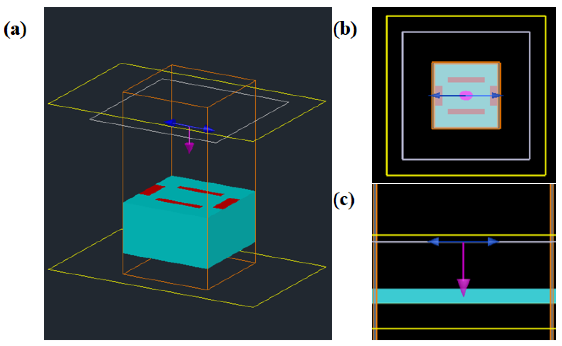
2. Design and Mechanism

The schematic diagram of the graphene-based dual-frequency terahertz sensor is shown in Figure 1a. The sensor is a classical sandwich structure consisting of a single-layer patterned graphene on the top, an intermediate dielectric layer, and a metal substrate at the bottom. Graphene is designed as an array of four strips to enhance the coupling effect with incident light and excite plasma resonance. It is known that plasma is very sensitive to external electromagnetic fields. When the external dielectric environment changes, the resonance peak will give a frequency shift, thereby achieving a sensing effect. The intermediate layer is designed to isolate the direct interaction between the gold substrate and graphene. Meanwhile, an appropriate intermediate material can adjust the impedance matching between the incident wave and the metamaterial, further enhancing the absorption of the incident wave. It has been reported that TOPAS can maintain a stable dielectric constant and has lower absorption losses in the terahertz frequency band. Therefore, a copolymer of cyclic olefins (TOPAS) with a relative dielectric constant of 2.35 and a thickness of 11 μm is chosen as the intermedium in our work. Gold film serves as a substrate to prevent the transmission of terahertz waves and can also provide support for the device. Figure 1b is the top view of the unit cell. Figure 1c depicts the geometric parameters of the unit cell. The four strips can be divided into two parallel groups, and the corresponding lengths and widths are marked as L1, d1, L2, and d2. The periodicity in x and y directions is the same and labeled as p.
A surface conductivity model is employed to numerically simulate monolayer graphene, and the surface conductivity σ(ω) can be calculated by using the Kubo formula [31]:
σ ( ω , μ c , τ , T ) = σ intra   ( ω , μ c , τ , T ) + σ inter   ( ω , μ c , τ , T )
σ intra ( ω ) = i ω + i / τ 2 e 2 k B T π 2 ln [ 2 cosh ( μ c 2 k B T ) ] σ inter ( ω ) = e 2 4 2 [ 1 2 + 1 π arctan ( ω 2 μ c 2 k B T ) i 2 π ln ( ω + 2 μ c ) 2 ( ω 2 μ c ) 2 + 4 ( k B T ) 2 ]
where σinter comes from the contribution of interband transitions, and σintra comes from the contribution of intraband transitions. ω is the angular frequency of the electromagnetic wave, kB is the Boltzmann constant, ħ = h/2π is the reduced Planck constant, and T is the absolute temperature at 300 K. e is the charge of an electron. τ is the relaxation rate and can be calculated as τ = μ μ c / e V f 2 , where μ is the electron mobility and V f is the Fermi velocity. The Fermi level of graphene is labeled as μc. In the terahertz frequency domain, the photon energy satisfies ħω << μc and μc >> kBT; the photon energy is much smaller than the Fermi level. Therefore, Formula (1) can be simplified to a quasi-Drude model [31]:
σ g σ i n t r a ( ω ) = e 2 μ c π 2 i ( ω + i / τ )
The variation in the trends of the real and imaginary parts of σ g under a different Fermi level μc is investigated and shown in Figure 2a,b. It can be observed that the real part of σ g decreases with the frequency increasing, which can be attributed to the electronic response of graphene. The imaginary part initially increases and then decreases with frequency, which is caused by the energy dissipation of graphene. When the operating frequency is fixed, both the real and imaginary parts of the conductivity increase with the increase in Fermi level, and the density of the charge carriers in graphene is responsible for this phenomenon.
The proposed sensor is studied by using Lumerical FDTD software (version 2019, Canonsburg, PA, USA). Figure 3 shows the simulation model established in FDTD. The plane wave is selected as the incident wave, the periodic boundary conditions are set in the x-axis and y-axis directions, and the z-direction boundary condition is set as the perfect matching layer (PML); the adaptive mesh and local mesh refinement are used to improve the simulation accuracy. Different monitors are added to the simulation model to collect the data of transmission, reflection, and field intensity distribution. By calculating the reflection coefficient S11 and the transmittance coefficient S21, the absorption rate can be calculated as A(ω) = 1 − R(ω) − T(ω) = 1 − |S11|2 − |S21|2, where R(ω) and T(ω) are reflectance and transmittance, respectively.

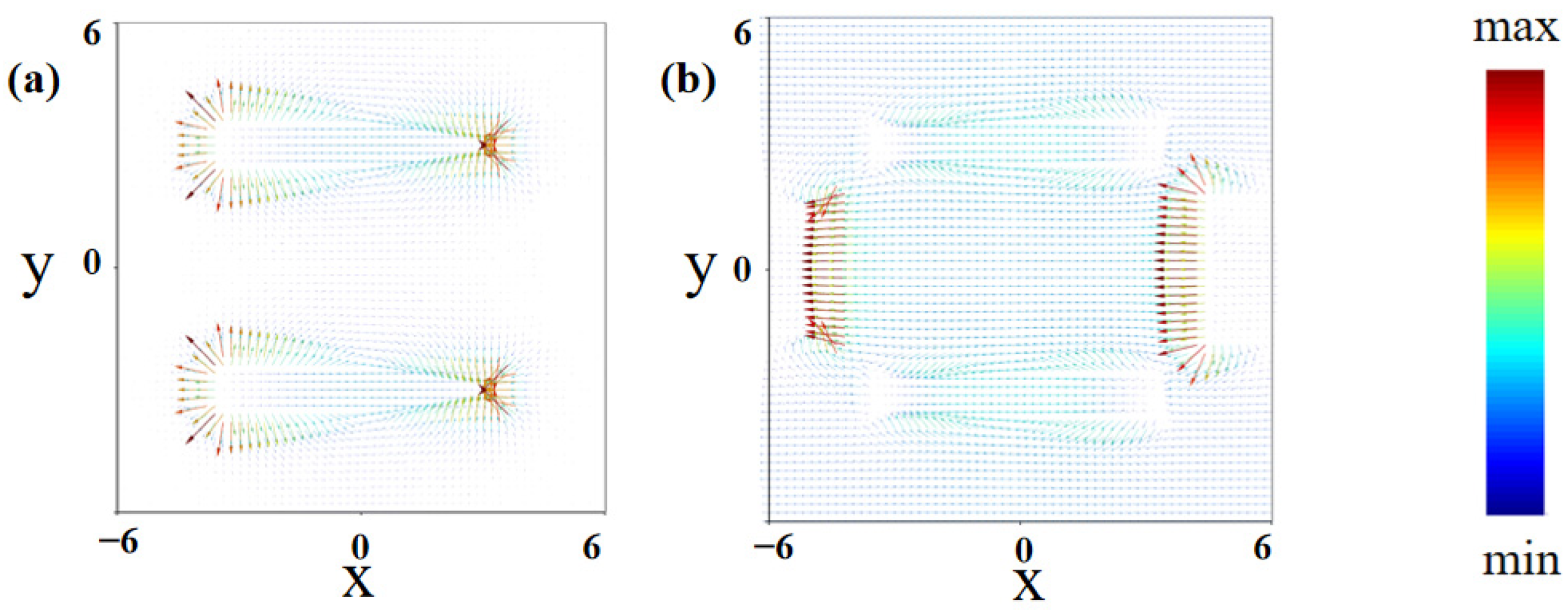
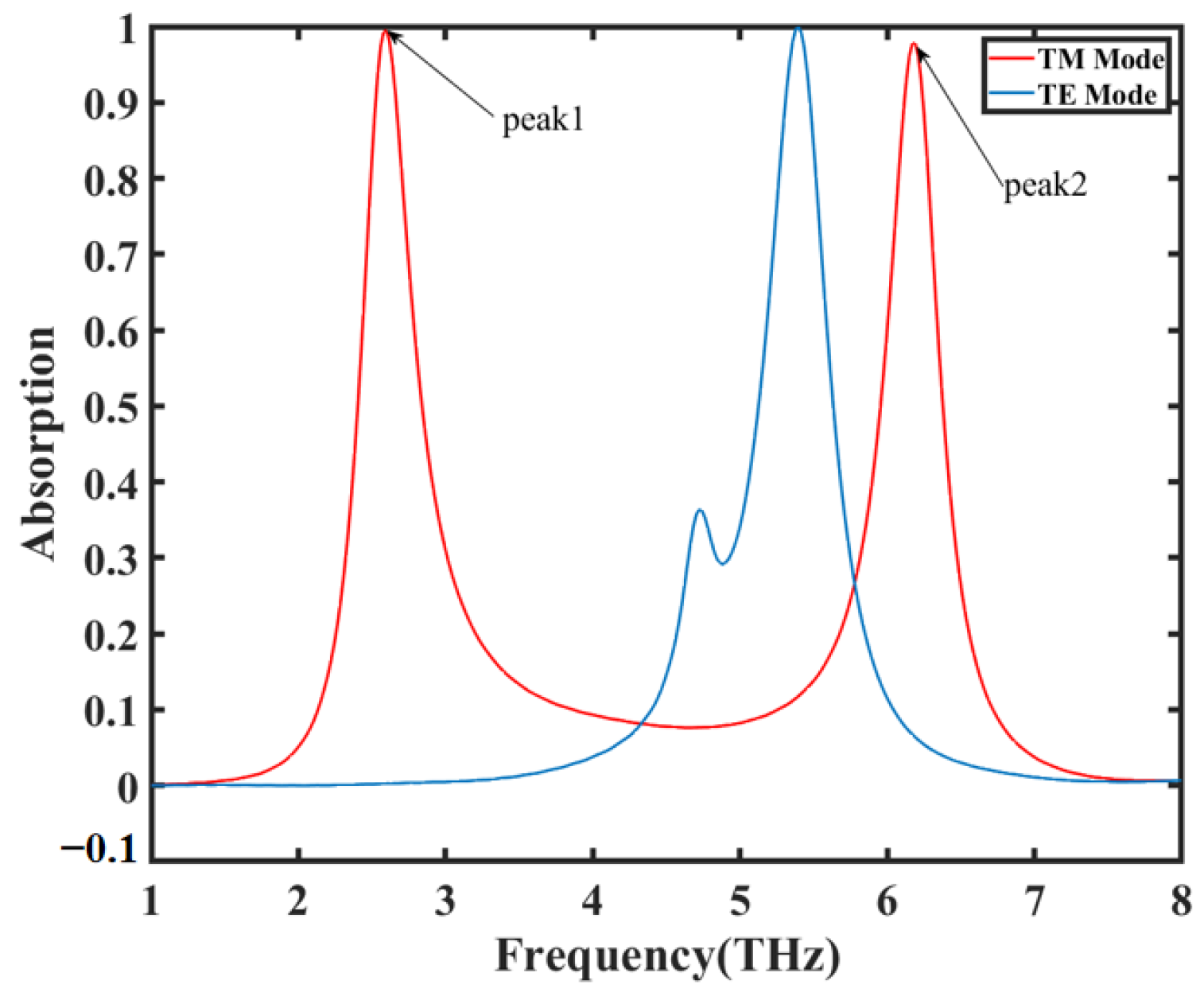
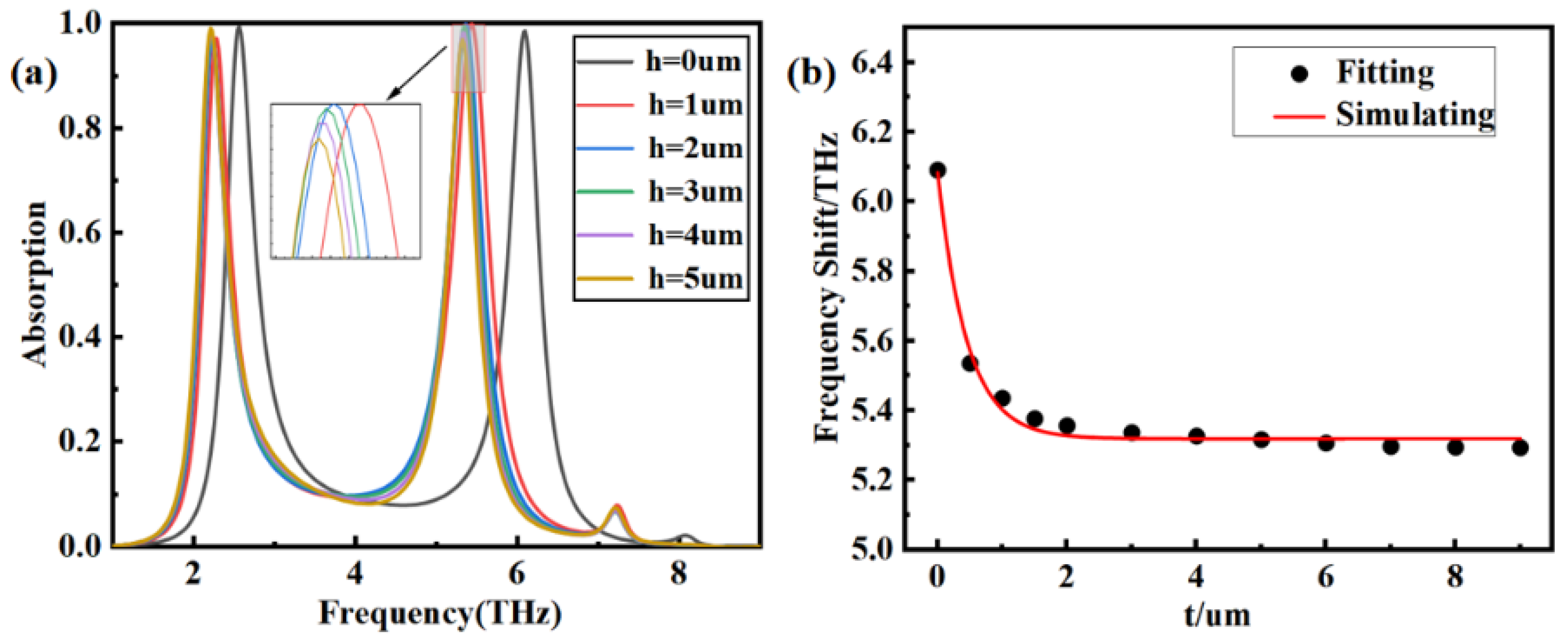
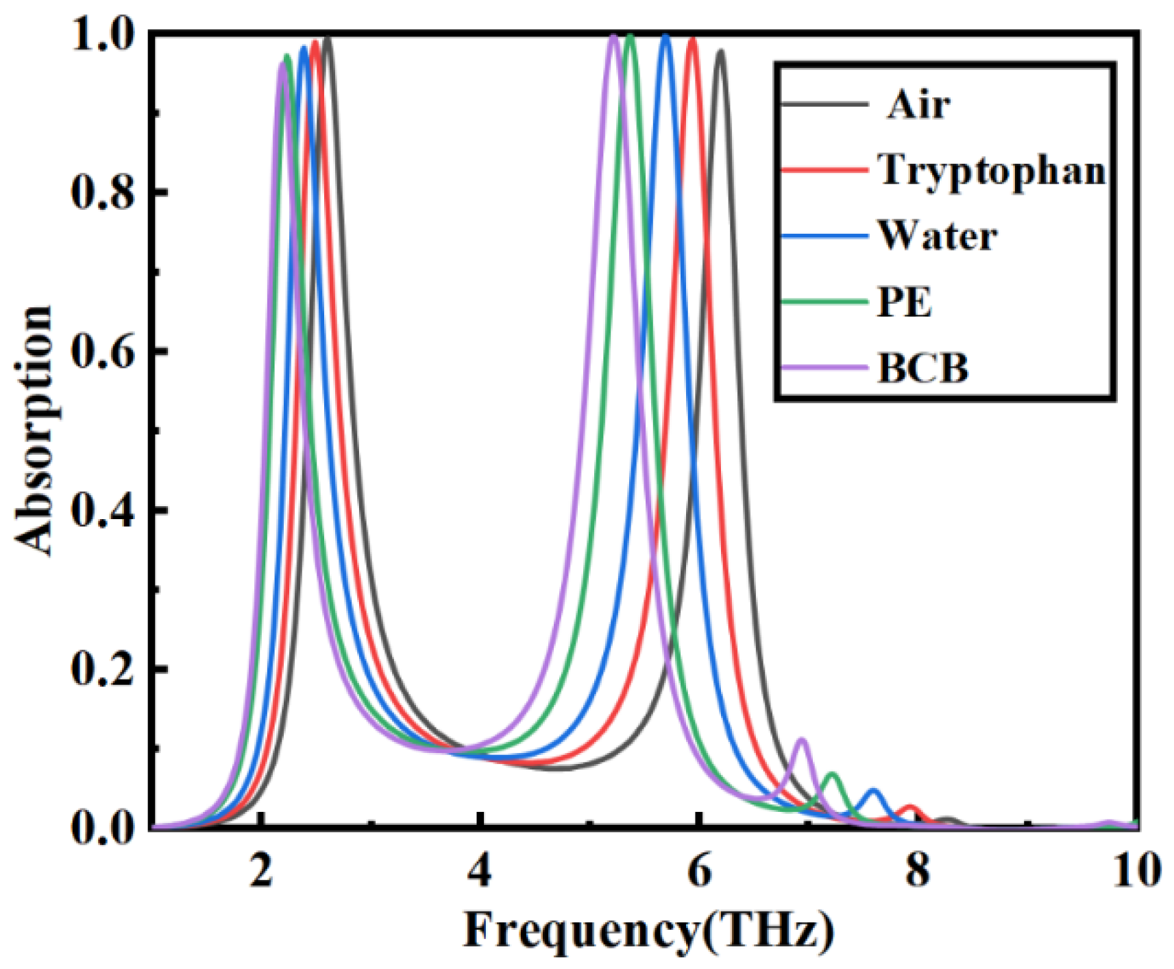
3. Results and Discussion

The impact of the geometric parameters of graphene pattern on sensing performance is studied and analyzed, while the Fermi level of graphene is set to be 0.8 eV. Meanwhile, in order to facilitate the description of dual-frequency peaks, the low-frequency resonance peak at 2.58 THz is labeled as P1 and the high-frequency resonance peak at 6.07 THz is labeled as P2.
Figure 4a shows the effect of L1 on P1 and P2 in the condition of transverse magnetic (TM) polarization when L2 = 3.7 μm, d1 = 1 μm, and d2 = 1.5 μm. It can be observed that as L1 gradually increases from 3 µm to 8 µm, there is an apparent redshift for P1, while P2 remains nearly unchanged. The bandwidth of P1 narrows as L1 increases. Figure 4b shows the effect of d1 on P1 and P2 when L1 = 7 μm. As d1 increases from 1 µm to 5 µm, both the amplitude and position of P1 and P2 are affected. For P1, the absorption rate significantly decreases, the position of peak shifts to a higher frequency, and the bandwidth widens. For P2, the absorption rate also decreases and the bandwidth widens, but the position of the peak shifts to a lower frequency. The influence of the length (L2) and width (d2) of the graphene strips parallel to the y-axis on P1 and P2 is studied and shown in Figure 4c,d when L1 = 7 μm and d1 = 1 μm. It is clear that the changes in d2 and L2 have a relatively weak impact on P1. For P2, as L2 increases, the absorption rate slightly decreases, and the bandwidth slightly widens. However, as d2 increases, the P2 peak shows a significant blue shift, and the bandwidth widens. These results illustrate that P1 is generated mainly due to the interaction between two lateral graphene strips and terahertz, while P2 is due to the longitudinal graphene strips and terahertz.
To investigate the resonance mechanism of the proposed sensor, the distribution of the electric field and surface currents on the graphene surface at the condition of a normal incidence angle is analyzed and depicted in Figure 5 and Figure 6. Figure 5a,b depict the electric field at resonance frequencies of 2.58 THz (P1) and 6.07 THz (P2) under TM polarized excitation in the x-y plane. Figure 5c,d depict the electric field in the x-z plane, respectively. As shown in Figure 5a,c at the resonance frequency of 2.58 THz (P1), the electric field is mainly concentrated at both ends of the graphene strips parallel to the x-axis, exhibiting characteristics of localized plasmon excitations. As shown in Figure 6a, the surface current generated at 2.58 THz is mainly concentrated on the graphene strips parallel to the y-axis, and the current propagates in the direction of the x-axis. The aggregation of positive and negative charges forms a strong electric dipole resonance. Similarly, at a resonance frequency of 6.07 THz, as shown in Figure 5b,d, the electric field is mainly concentrated at the edge of the graphene strips parallel to the y-axis, forming an electric dipole resonance. The corresponding surface current, as shown in Figure 6b, is mainly concentrated on graphene strips parallel to the y-axis and propagates along the direction of the x-axis.
The unique tunable properties of graphene can be achieved by applying a bias voltage to change its Fermi level, which can affect the carrier concentration and achieve dynamic tunability of the sensor. The relationship between the Fermi level μc and the bias voltage Vg can be described as follows [32]:
| u c | = V f π | a 0 V g |
where a 0 = ε 0 ε h e d is the capacitance of the structural model, ε 0 is the vacuum intermediate constant, ε h is the dielectric constant, and d is the thickness of the middle dielectric layer. As shown in Figure 7, the structure parameters are set as L1 = 7 μm, L2 = 3.7μm, d1 = 1 μm, and d2 = 1.5 μm; when the Fermi level (μc) increases from 0.4 eV to 0.8 eV, both of the dual-frequency absorption peaks give remarkably blue shift and bandwidth widening. P1 moves from 1.905 THz to 2.857 THz, while P2 moves from 4.444 THz to 6.805 THz. The reason for this is an enhancement of plasma resonance, which originated from the increasing in the density of the charge carriers in graphene. The wave vector of the plasma polarization exaction in graphene can be described as k s p p h f r 2 / ( 2 α 0 E f c ) , where fr is the resonant frequency and α 0 is the fine structure constant. The frequency of graphene plasmon resonance is related to the Fermi level. When μc reaches 0.7 eV, plasmon resonance reaches its maximum. As the Fermi level continues to increase, the frequency of the absorption peak gradually deviates from the plasmon resonance region, and the amplitude of the peak begins to decrease.
The sensitivity of TE (transverse electric) and TM (transverse magnetic) polarization for the designed sensor is also investigated and shown in Figure 8. It is clear that the two different polarization modes have a significant impact on the absorption peak. On the one hand, the asymmetry of the designed structure makes the sensor sensitive to the polarization angle. On the other hand, the dual-frequency resonance peaks are affected by different strips. For four strips in a single unit cell, two are parallel to the x-axis and two are parallel to the y-axis. When interacting with incident light, the local plasma resonance excited is different, thus leading to differences in the absorption peak.
To characterize the application performance of the proposed device, a layer of analyte is considered on the top of the sensor. The effect of the analyte’s thickness on sensor performance is studied and shown in Figure 9a. Here, frequency shift (FS) is defined as FS = ftfr, where ft is the resonant frequency when covering a layer of analyte with a thickness of t, and fr is the resonant frequency when there is no analyte. In Figure 9a, the analyte’s refractive index is assumed to be 1.5; both of the P1 and P2 tend to show as redshifted as the thickness increases. Figure 9b shows the frequency shifts corresponding to the thicknesses. The red solid line is the result of exponential function fitting. As can be seen, as the analyte thickness increases, the frequency shift does not always increase but decreases exponentially and gradually reaches saturation after the thickness exceeds 2 μm. The outcomes are consistent with actual measurements when the thickness exceeds the saturation thickness, and the frequency shift is so weak that it can be ignored, which is also an important aspect of ensuring stable sensor measurements.
The influence of the refractive index of the analyte on the sensor performance is investigated when the thickness of the analyte is fixed at t = 2 μm. According to the results depicted in Figure 10a, the dual-frequency peaks have an obvious tendency to shift towards lower frequencies with an increase in the refractive index. The relationship between the dielectric constant and the resonant frequency is shown in Formula (4) [33]:
f r = e 2 π h μ c η ε 0 ε r 1 + ε r 2 P
where P is denoted as the period of the unit structure, and ε r 1 and ε r 2 are represented as the dielectric constants of different media, respectively. The trend of the frequency shift of P1 and P2 is shown in Figure 10b, which clearly shows that the frequency shift increases almost linearly with the increase in the refractive index. The curves’ steepness represents the sensor’s sensitivity, providing a more intuitive reflection of the trends in resonance peak variations. As the refractive index of the analyte changes, the absorption rate of the dual-frequency absorption peaks can always be maintained above 90%, with almost no change in amplitude. However, the phase of peak P1 shifts from 2.6 THz to 2.12 THz, and P2 shifts from 6.17 THz to 5.15 THz. Apparently, the phase shift of P2 is more pronounced than P1; this is primarily due to the different dispersion effects of the material at high or low frequencies.
To evaluate the performance of the proposed sensor quantitatively, three performance indexes are introduced, which are sensitivity (S), figure of merit (FOM) value, and quality factor (Q). The sensitivity is defined as S = Δf/Δn (THz/RIU). Δf denotes the frequency shift from f1 to f2, which means Δf = |f1f2|. Δn represents the change in the refractive index from n1 to n2, that means Δn = |n1 − n2|, and the unit is THz/RIU (Refractive Index Unit, RIU). The value of FOM is a dimensionless parameter and defined as FOM = S/FWHM, where FWHM represents the full width at half maximum of the resonance peak. Q is an important parameter of the sensor. Sensors with high Q values have high sensitivity and stability, which can provide more accurate and reliable measurement results. Q is defined and expressed as Q = f/FWHM. For the proposed sensor, the sensitivity of P1 is S1 = 714 GHz/RIU with a quality factor of Q1 = 11.8 and an FOM value of 1.63 RIU−1. The sensitivity of P2 is calculated to be S2 = 1.627 THz/RIU, with a quality factor of Q2 = 29.6 and an FOM value of 3.9 RIU−1.
The results obtained in this paper are compared with similar works in Refs. [26,27,29,34,35,36,37,38] shown in Table 1. Compared with Refs. [29,38], in terms of pattern structure, our design is simpler and easier to fabricate. Compared with Ref. [37], the proposed sensor not only has a wider operable frequency band range, higher sensitivity, and higher Q and FOM values but can also be dynamically adjusted by the introduction of graphene. Compared with Refs. [34,35,36], the proposed sensor has dual-frequency resonance peaks and better sensing performance. Although Ref. [26] has a higher sensitivity and higher Q and FOM values, it adopts a metal structure and can only achieve the passive modulation of terahertz waves.
To illustrate the specific application of the proposed sensor, several common substances are tested, including air (RI = 1.0), tryptophan powder (RI = 1.17), water (RI = 1.33), polyethylene (PE) powder (RI = 1.5), and Benzocy clobutene (BCB, RI = 1.65). The results are shown in Figure 11. It can be observed that the resonance peak undergoes a significant redshift as the refractive index increases. The designed sensor can also be applied for practical applications in the biomedical field. Usually, biological samples attached to the sensor’s surface exhibit different dielectric constants under an external electric field, meaning that the physical properties of the surface substances can be analyzed. For example, the content of water in cells is a significant factor affecting the dielectric constant between tumor cells and healthy cells. Normal cells have a content of water of about 30–70% with a refractive index of 1.36, while basal carcinoma cells have a high content of water of 80% and a refractive index of about 1.38. Tumor cells with abundant vascularization and edema have been reported to exhibit high cellular water content. Since the vibration modes of water molecules fall in the terahertz frequency domain (the most vital resonance frequencies are 5.6 and 1.5 THz), the terahertz sensor designed in this study has essential significance in biomedicine, sample detection, and environment monitoring.

4. Conclusions

A dual-frequency terahertz sensor based on graphene and absorption mechanism is proposed. By analyzing the structural parameters of the top graphene layers, the optimal parameters are identified to enhance the mutual coupling between graphene and terahertz waves. The absorption rate exceeds 99% at resonant frequencies of 2.86 and 6.07 THz. The sensitivity of P1 is calculated to be 714 GHz/RIU, with a quality factor of Q1 = 11.8 and an FOM value of 1.63 RIU−1. The sensitivity of P2 was calculated to be 1.627 THz/RIU, with a quality factor of Q2 = 29.6 and an FOM value of 3.9 RIU−1. The sensing mechanism of the designed sensor is revealed by analyzing the electromagnetic field distribution. The performance of the sensor is analyzed for different refractive indices and different thicknesses of the analyte. Compared to similar research reported before, the present senor not only has a simple micro/nano-pattern but also exhibits superior sensing characteristics, such as a higher sensitivity and Q value. Meanwhile, compared to sensors made of metal, the designed sensor can be dynamically tuned. Therefore, the sensor has great potential application values in the fields of optical communication, material characterization, environmental monitoring, and biomedicine in the terahertz band.

Author Contributions

This manuscript was written by Y.Y. and M.F. The simulation was carried out by Y.Y., Y.N. and X.L. The analyses and discussions of these obtained results were carried out by M.F., S.G. and Z.W. All authors have read and agreed to the published version of the manuscript.

Funding

This work was supported by National Natural Science Foundation of China (No. 61805072, 62205101, and 62301211), Research Foundation for University Key Teacher of Henan Province (No. 2020GGJS084), Innovative Funds Plan of Henan University of Technology (No. 2022ZKCJ15), Open Project of Key Laboratory of Ministry of Education (No. KFJJ-2021-105), and Research Foundation for Key Teacher of Henan University of Technology.

Institutional Review Board Statement

Not applicable.

Informed Consent Statement

Not applicable.

Data Availability Statement

All data that support the findings of this study are included within the article.

Conflicts of Interest

The authors declare no conflicts of interest.

References

  1. Nguyen, D.M.; Lee, D.; Rho, J. Control of light absorbance using plasmonic grating based perfect absorber at visible and near-infrared wavelengths. Sci. Rep. 2017, 7, 2611. [Google Scholar] [CrossRef]
  2. Ferguson, B.; Zhang, X.-C. Materials for terahertz science and technology. Nat. Mater. 2002, 1, 26–33. [Google Scholar] [CrossRef]
  3. Chen, Z.; Han, C.; Wu, Y.; Li, L.; Huang, C.; Zhang, Z.; Wang, G.; Tong, W. Terahertz wireless communications for 2030 and beyond: A cutting-edge frontier. IEEE Commun. Mag. 2021, 59, 66–72. [Google Scholar] [CrossRef]
  4. Song, H.J.; Nagatsuma, T. Present and future of terahertz communications. IEEE Trans. Terahertz Sci. Technol. 2011, 1, 256–263. [Google Scholar] [CrossRef]
  5. Zhang, M.; Pirandola, S.; Delfanazari, K. Millimetre-waves to terahertz SISO and MIMO continuous variable quantum key distribution. IEEE Trans. Quantum Eng. 2023, 4, 4100410. [Google Scholar] [CrossRef]
  6. Active terahertz modulator and slow light metamaterial devices with hybrid graphene–superconductor photonic integrated circuits. Nanomaterials 2021, 11, 2999. [CrossRef]
  7. Nagatsuma, T.; Horiguchi, S.; Minamikata, Y.; Yoshimizu, Y.; Hisatake, S.; Kuwano, S.; Yoshimoto, N.; Terada, J.; Takahashi, H. Terahertz wireless communications based on photonics technologies. Opt. Express 2013, 21, 23736–23747. [Google Scholar] [CrossRef]
  8. Wiersma, D.S. Disordered photonics. Nat. Photonics 2013, 7, 188–196. [Google Scholar] [CrossRef]
  9. Delfanazari, K.; Klemm, R.A.; Joyce, H.J.; Ritchie, D.A.; Kadowaki, K. Integrated, portable, tunable, and coherent terahertz sources and sensitive detectors based on layered superconductors. Proc. IEEE 2020, 108, 721–734. [Google Scholar] [CrossRef]
  10. Delfanazari, K.; Asai, H.; Tsujimoto, M.; Kashiwagi, T.; Kitamura, T.; Yamamoto, T.; Sawamura, M.; Ishida, K.; Watanabe, C.; Sekimoto, S.; et al. Tunable terahertz emission from the intrinsic Josephson junctions in acute isosceles triangular Bi2Sr2CaCu2O8+δ mesas. Opt. Express 2013, 21, 2171–2184. [Google Scholar] [CrossRef]
  11. Samizadeh Nikoo, M.; Jafari, A.; Perera, N.; Zhu, M.; Santoruvo, G.; Matioli, E. Nanoplasma-enabled picosecond switches for ultrafast electronics. Nature 2020, 579, 534–539. [Google Scholar] [CrossRef] [PubMed]
  12. Kalhor, S.; Savel’ev, S.; Delfanazari, K. Engineering ultrastrong coupling between Josephson plasmon polaritons and subwavelength microcavity arrays in silicon/van der Waals layered superconductor heterostructure for terahertz hybrid circuit cavity quantum electrodynamics. Phys. Rev. B 2022, 106, 245140. [Google Scholar] [CrossRef]
  13. Xiao, S.; Wang, T.; Liu, T.; Yan, X.; Li, Z.; Xu, C. Active modulation of electromagnetically induced transparency analogue in terahertz hybrid metal-graphene metamaterials. Carbon 2018, 126, 271–278. [Google Scholar] [CrossRef]
  14. Kordi, M.; Mirsalehi, M.M. Investigation of a metamaterial slab lens and an imaging system based on an ellipsoidal cavity. Appl. Opt. 2017, 56, 4772–4778. [Google Scholar] [CrossRef] [PubMed]
  15. Khavasi, A.; Chrostowski, L.; Lu, Z.; Bojko, R. Significant crosstalk reduction using all-dielectric CMOS-compatible metamaterials. IEEE Photonics Technol. Lett. 2016, 28, 2787–2790. [Google Scholar] [CrossRef]
  16. Legaria, S.; Teniente, J.; Kuznetsov, S.; Pacheco-Pena, V.; Beruete, M. Highly efficient focusing of terahertz waves with an ultrathin superoscillatory metalens: Experimental demonstration. Adv. Photonics Res. 2021, 2, 2000165. [Google Scholar] [CrossRef]
  17. Schurig, D.; Mock, J.J.; Justice, B.J.; Cummer, S.A.; Pendry, J.B.; Starr, A.F.; Smith, D.R. Metamaterial electromagnetic cloak at microwave frequencies. Science 2006, 314, 977–980. [Google Scholar] [CrossRef]
  18. Strikwerda, A.C.; Zalkovskij, M.; Lorenzen, D.L.; Krabbe, A.; Lavrinenko, A.V.; Jepsen, P.U. Metamaterial composite bandpass filter with an ultra-broadband rejection bandwidth of up to 240 terahertz. Appl. Phys. Lett. 2014, 104, 191103. [Google Scholar] [CrossRef]
  19. Fu, M.X.; Wang, J.Y.; Guo, S.S.; Wang, Z.Y.; Yang, P.X.; Niu, Y.Y. A polarization-insensitive broadband terahertz absorber using patterned graphene. Nanomaterials 2022, 12, 3763. [Google Scholar] [CrossRef]
  20. Bonaccorso, F.; Sun, Z.; Hasan, T.; Ferrari, A.C. Graphene photonics and optoelectronics. Nat. Photonics 2010, 4, 611–622. [Google Scholar] [CrossRef]
  21. Wen, Q.Y.; Tian, W.; Mao, Q.; Chen, Z.; Liu, W.W.; Yang, Q.H.; Sanderson, M.; Zhang, H.W. Graphene based all-optical spatial terahertz modulator. Sci. Rep. 2014, 4, 7409. [Google Scholar] [CrossRef]
  22. Hu, D.; Meng, T.H.; Wang, H.Y.; Fu, M.X. Actively tunable dual-broadband graphene-based terahertz metamaterial absorber. Chin. Phys. B 2021, 30, 126101. [Google Scholar] [CrossRef]
  23. He, Z.; Li, L.; Ma, H.; Pu, L.; Xu, H.; Yi, Z.; Cao, X.; Cui, W. Graphene-based metasurface sensing applications in terahertz band. Results Phys. 2021, 21, 103795. [Google Scholar] [CrossRef]
  24. Pianelli, A.; Kowerdziej, R.; Dudek, M.; Sielezin, K.; Olifierczuk, M.; Parka, J. Graphene-based hyperbolic metamaterial as a switchable reflection modulator. Opt. Express 2020, 28, 6708–6718. [Google Scholar] [CrossRef]
  25. Dudek, M.; Kowerdziej, R.; Pianelli, A.; Parka, J. Graphene-based tunable hyperbolic microcavity. Sci. Rep. 2021, 11, 74. [Google Scholar] [CrossRef]
  26. Wang, B.X.; Huang, W.Q.; Wang, L.L. Ultra-narrow terahertz perfect light absorber based on surface lattice resonance of a sandwich resonator for sensing application. RSC Adv. 2017, 7, 42956–42963. [Google Scholar] [CrossRef]
  27. Hu, D.; Meng, T.; Wang, H.; Ma, Y.; Zhu, Q. Ultra-narrow-band terahertz perfect metamaterial absorber for refractive index sensing application. Results Phys. 2020, 19, 103567. [Google Scholar] [CrossRef]
  28. Chen, T.; Jiang, W.; Yin, X. Dual-band ultrasensitive terahertz sensor based on tunable graphene metamaterial absorber. Superlattices Microstruct. 2021, 154, 106898. [Google Scholar] [CrossRef]
  29. Nickpay, M.R.; Danaie, M.; Shahzadi, A. Graphene-based metamaterial absorber for refractive index sensing applications in terahertz band. Diam. Relat. Mater. 2022, 130, 109539. [Google Scholar] [CrossRef]
  30. Li, L.; Ge, H.; Jiang, Y.; Li, G.; Wang, F.; Lv, M.; Ji, X.; Jia, Z.; Li, Z.; Zhang, Y. A four-band terahertz metamaterial sensor based on symmetric E-shaped structure. Coatings 2022, 12, 1694. [Google Scholar] [CrossRef]
  31. Thongrattanasiri, S.; Koppens, F.H.; De Abajo, F.J.G. Complete optical absorption in periodically patterned graphene. Phys. Rev. Lett. 2012, 108, 047401. [Google Scholar] [CrossRef]
  32. Zhan, Y.; Fan, C. Investigation on the tunable and polarization sensitive three-band terahertz graphene metamaterial absorber. Mater. Res. Express 2023, 10, 055802. [Google Scholar] [CrossRef]
  33. Gao, W.; Shi, G.; Jin, Z.; Shu, J.; Zhang, Q.; Vajtai, R.; Ajayan, P.M.; Kono, J.; Xu, Q. Excitation and active control of propagating surface plasmon polaritons in graphene. Nano Lett. 2013, 13, 3698–3702. [Google Scholar] [CrossRef]
  34. Saadeldin, A.S.; Hameed, M.F.O.; Elkaramany, E.M.; Obayya, S.S. Highly sensitive terahertz metamaterial sensor. IEEE Sens. J. 2019, 19, 7993–7999. [Google Scholar] [CrossRef]
  35. Nickpay, M.R.; Danaie, M.; Shahzadi, A. Highly sensitive THz refractive index sensor based on folded split-ring metamaterial graphene resonators. Plasmonics 2021, 17, 237–248. [Google Scholar] [CrossRef]
  36. Qi, Y.; Zhang, Y.; Liu, C.; Zhang, T.; Zhang, B.; Wang, L.; Deng, X.; Bai, Y.; Wang, X. A tunable terahertz metamaterial absorber composed of elliptical ring graphene arrays with refractive index sensing application. Results Phys. 2020, 16, 103012. [Google Scholar] [CrossRef]
  37. Lu, X.; Ge, H.; Jiang, Y.; Zhang, Y. Design and analysis of a dual-band THz metamaterial sensor with high refractive index sensitivity. Front. Phys. 2022, 10, 973033. [Google Scholar] [CrossRef]
  38. Ge, J.; You, C.; Feng, H.; Li, X.; Wang, M.; Dong, L.; Veronis, G.; Yun, M. Tunable dual plasmon-induced transparency based on a monolayer graphene metamaterial and its terahertz sensing performance. Opt. Express 2020, 28, 31781–31795. [Google Scholar] [CrossRef]
Figure 1. Structure of the sensor. (a) Schematic view; (b) unit cell; (c) top view (x-y plane).
Nanomaterials 14 00378 g001
Figure 2. The real and imaginary parts of σ g . (a) Real part; (b) imaginary part.
Nanomaterials 14 00378 g002
Figure 3. Simulation model of the sensor established in FDTD. (a) Perspective view of the sensor; (b) the view of x-y plane; (c) the view of y-z plane.
Nanomaterials 14 00378 g003
Figure 4. The sensing performance with different geometrical parameters in TM mode. (a) Different L1; (b) different d1; (c) different L2; (d) different d2.
Nanomaterials 14 00378 g004
Figure 5. The electric field distribution at 2.58 THz and 6.07 THz, respectively. (a,b) are in the x-y plane; (c,d) are in the y-z plane.
Nanomaterials 14 00378 g005
Figure 6. Surface current distribution in TM mode at dual-frequency peaks. (a) At 2.58 THz; (b) at 6.07 THz.
Nanomaterials 14 00378 g006
Figure 7. The influence of Fermi level on dual-frequency absorption peaks.
Nanomaterials 14 00378 g007
Figure 8. The influence of TE and TM polarization modes on dual-frequency absorption peaks.
Nanomaterials 14 00378 g008
Figure 9. The influence of thickness of analyte on P1 and P2. (a) Effect of thickness on absorption spectra; (b) exponential function fitting curve.
Nanomaterials 14 00378 g009
Figure 10. The influence of refractive index on P1 and P2. (a) Absorption spectra; (b) the relationship between the refractive index and the positions of P1 and P2.
Nanomaterials 14 00378 g010
Figure 11. The influence of different analytes on the sensing performance.
Nanomaterials 14 00378 g011
Table 1. Comparison of the performance of sensors from other researchers.
Ref.PatternMaterialNumber of PeaksOperating Range
(THz)
Sensitivity (GHz/RIU)Quality Factor
(Q)
FOM
(RIU−1)
[34]Split ringGold–dielectric–gold11.5–330022.52.94
[35]Folded Split RingGraphene–SiO2–gold12–685113.763.33
[36]Elliptical ring Graphene–SiO213–101326/3.6
[27]cross-shaped patchGaAs–Cu12–2.51942637506
[26]Square Au ringGold–dielectric–gold12.5–3.52584442385
[37]Split ringGold–PTFE20.2–3730 10.172.52
[38]Two strips and ringGraphene–SiO231–6108316.23.78
[29]Split ring and ribbonGraphene–TOPAS–gold32–10179132.3547.046
Our workFour stripsGraphene–TOPAS–gold21–10162729.63.9
Disclaimer/Publisher’s Note: The statements, opinions and data contained in all publications are solely those of the individual author(s) and contributor(s) and not of MDPI and/or the editor(s). MDPI and/or the editor(s) disclaim responsibility for any injury to people or property resulting from any ideas, methods, instructions or products referred to in the content.

