
Optimization of Soft X-Ray Fresnel Zone Plate Fabrication Through Joint Electron Beam Lithography and Cryo-Etching Techniques

 , , , , and
Abstract
1. Introduction
2. Fabrication and Discussion
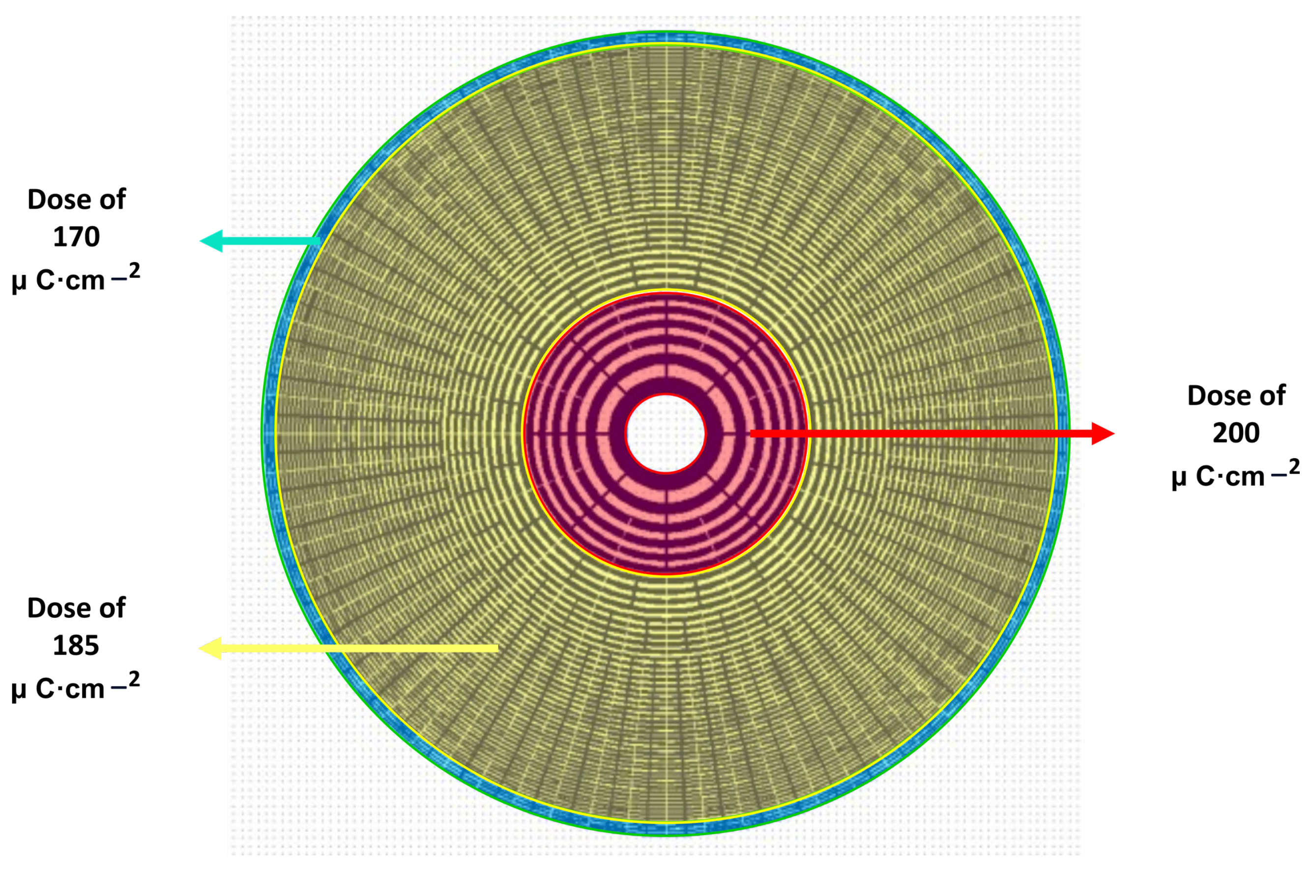
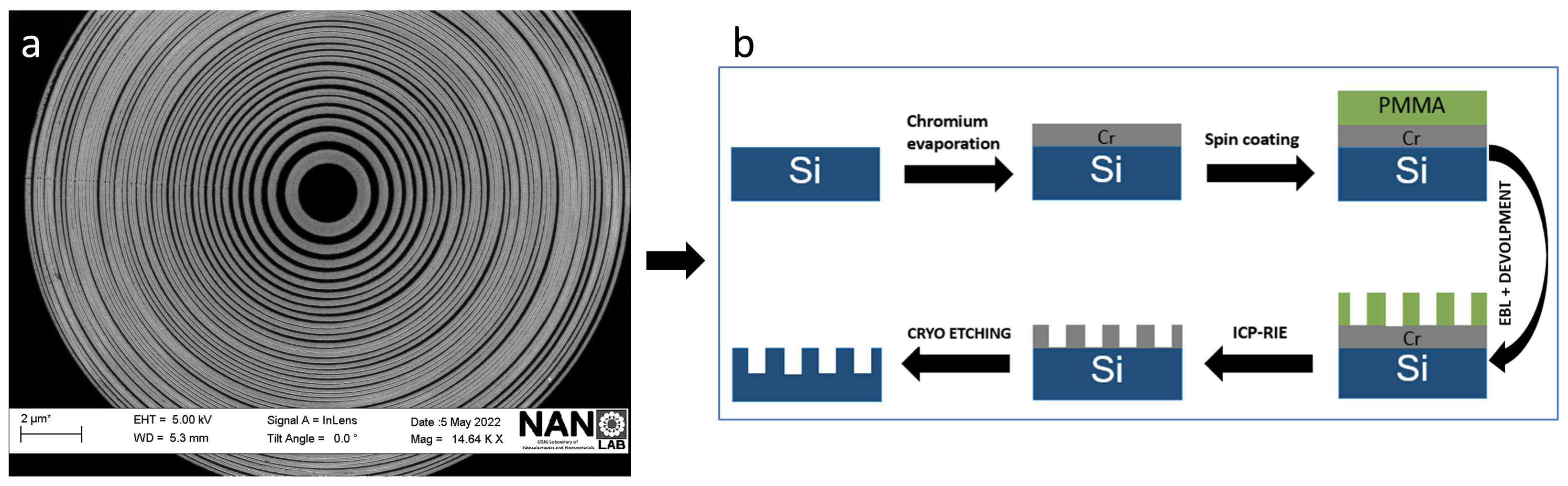
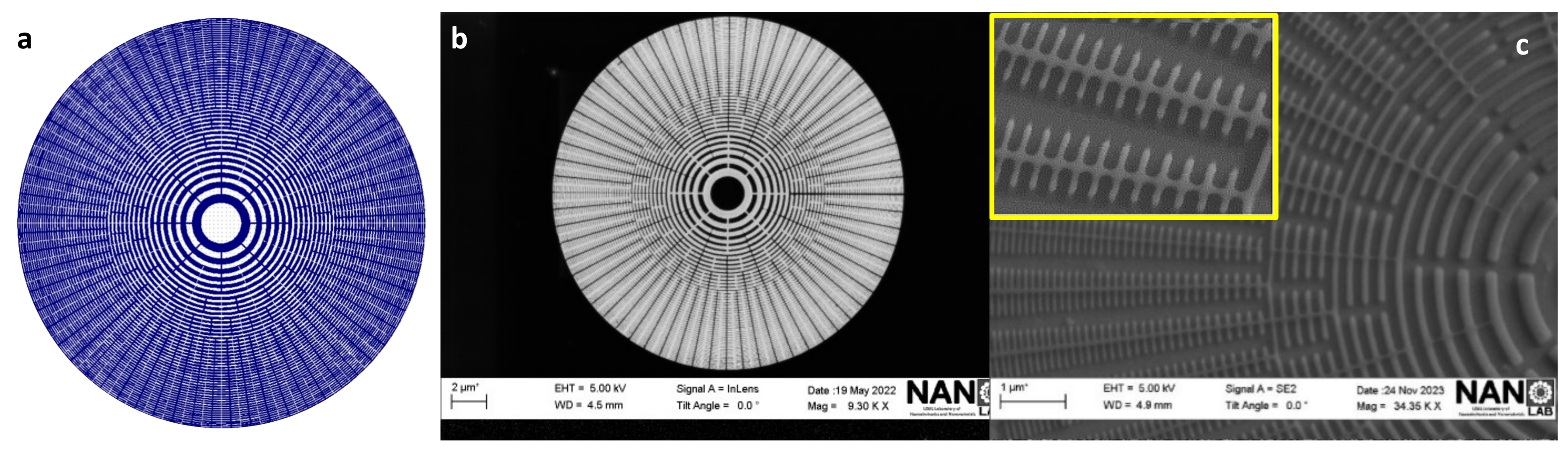
2.1. PMMA Mask Preparation
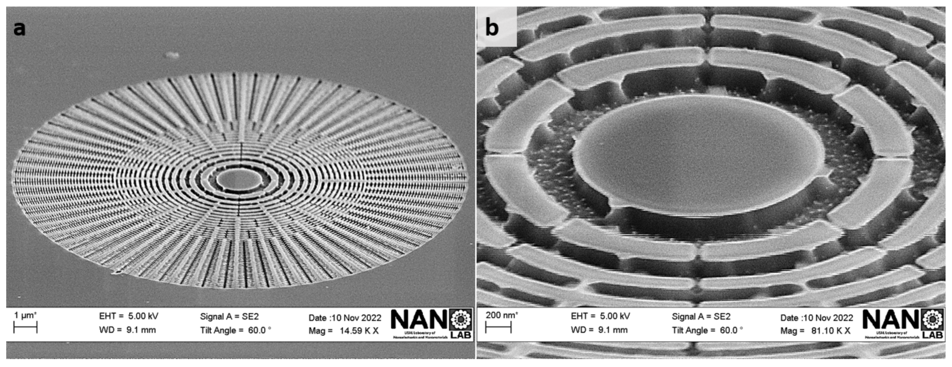
2.2. Chromium Mask Fabrication
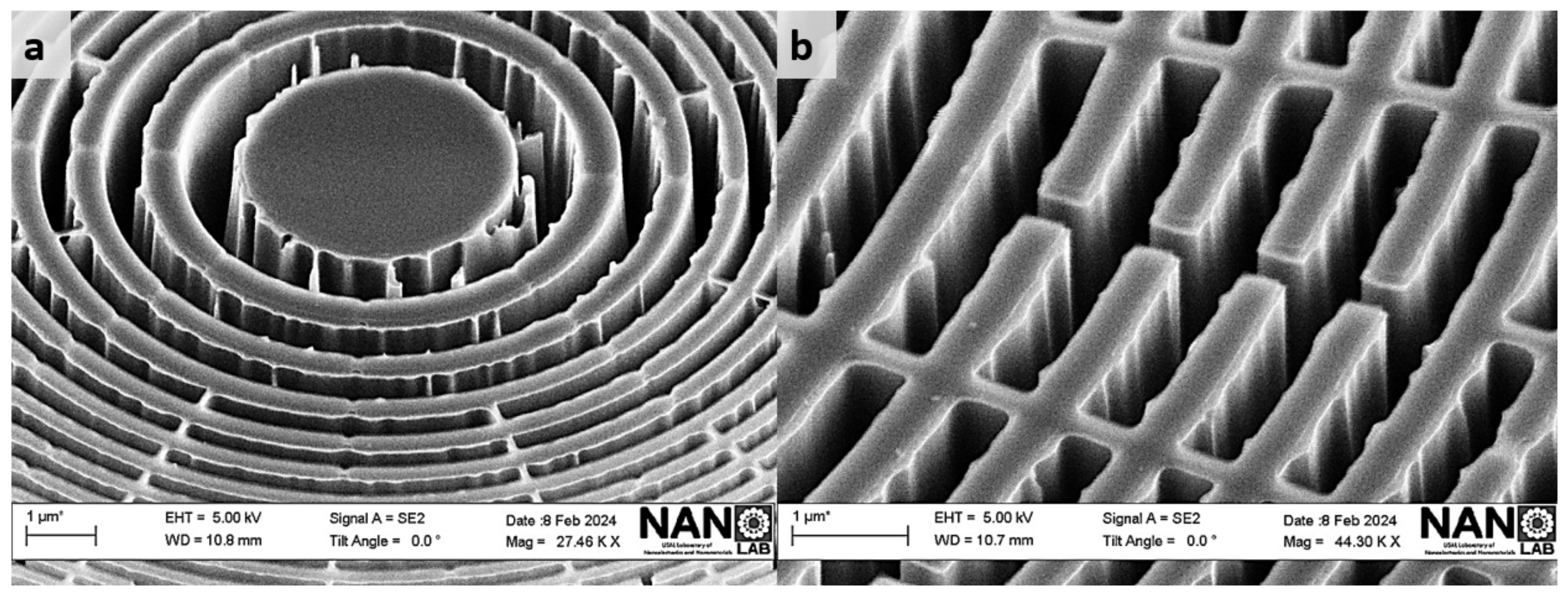
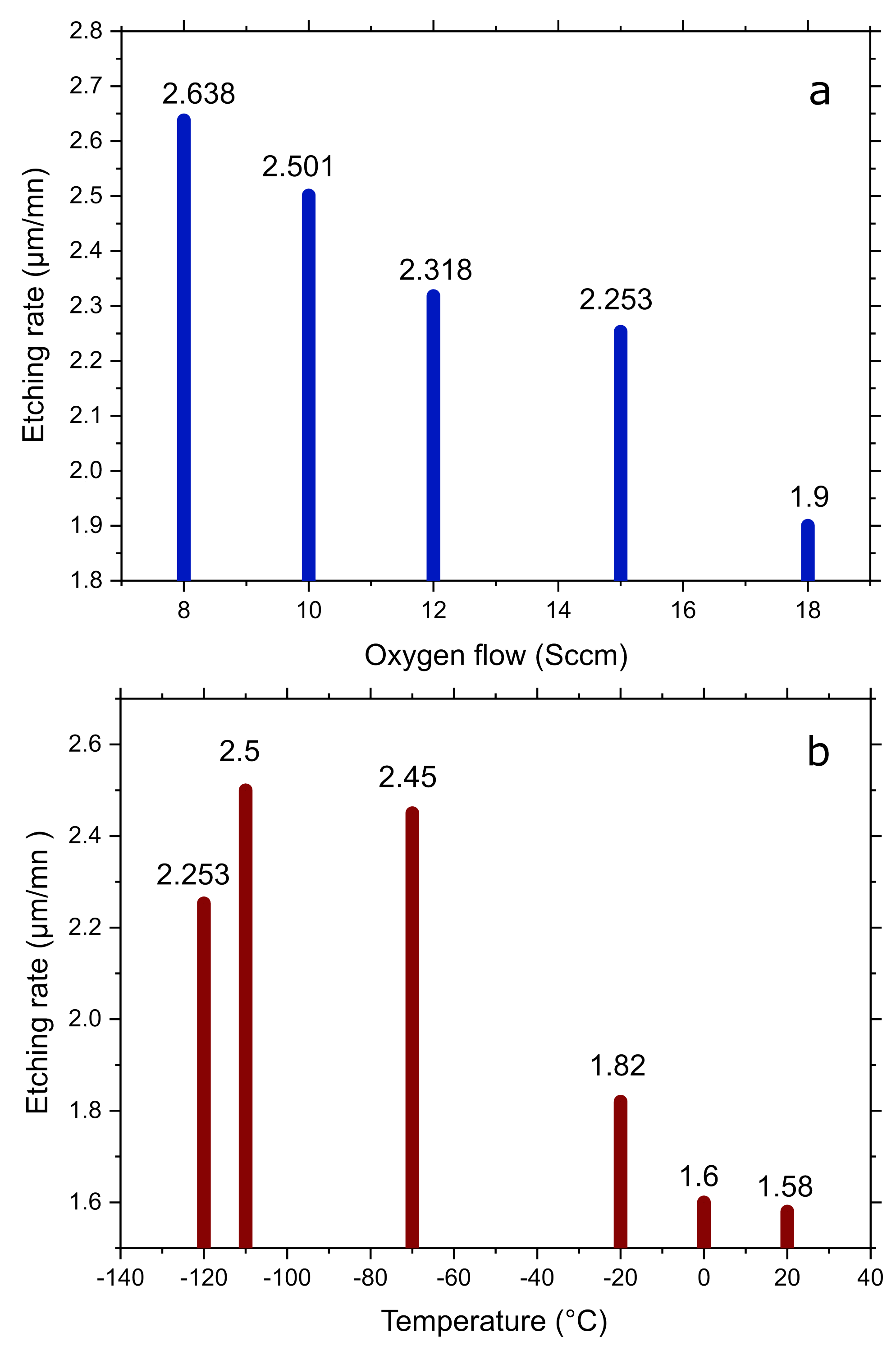
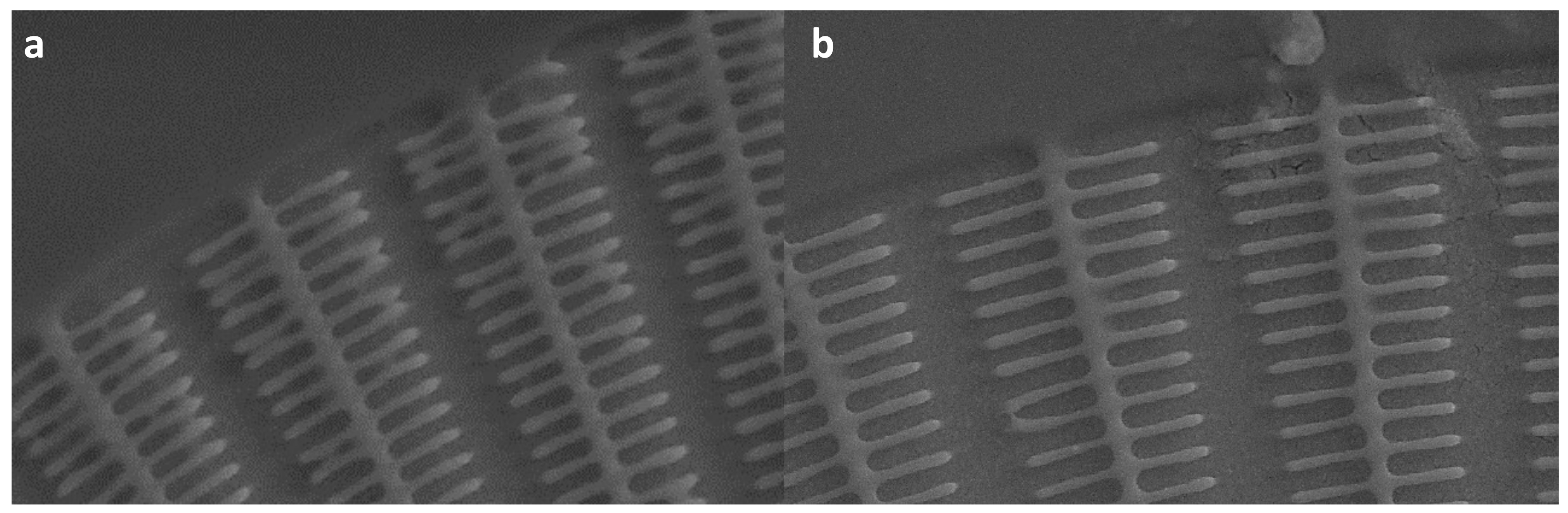
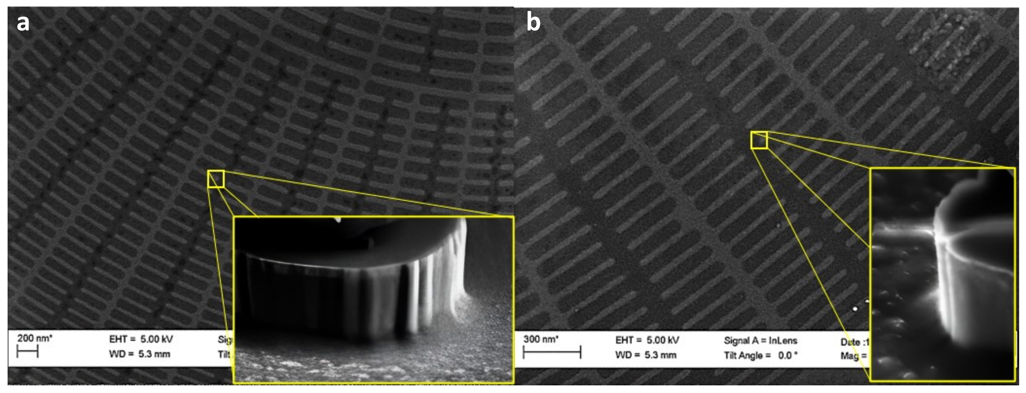
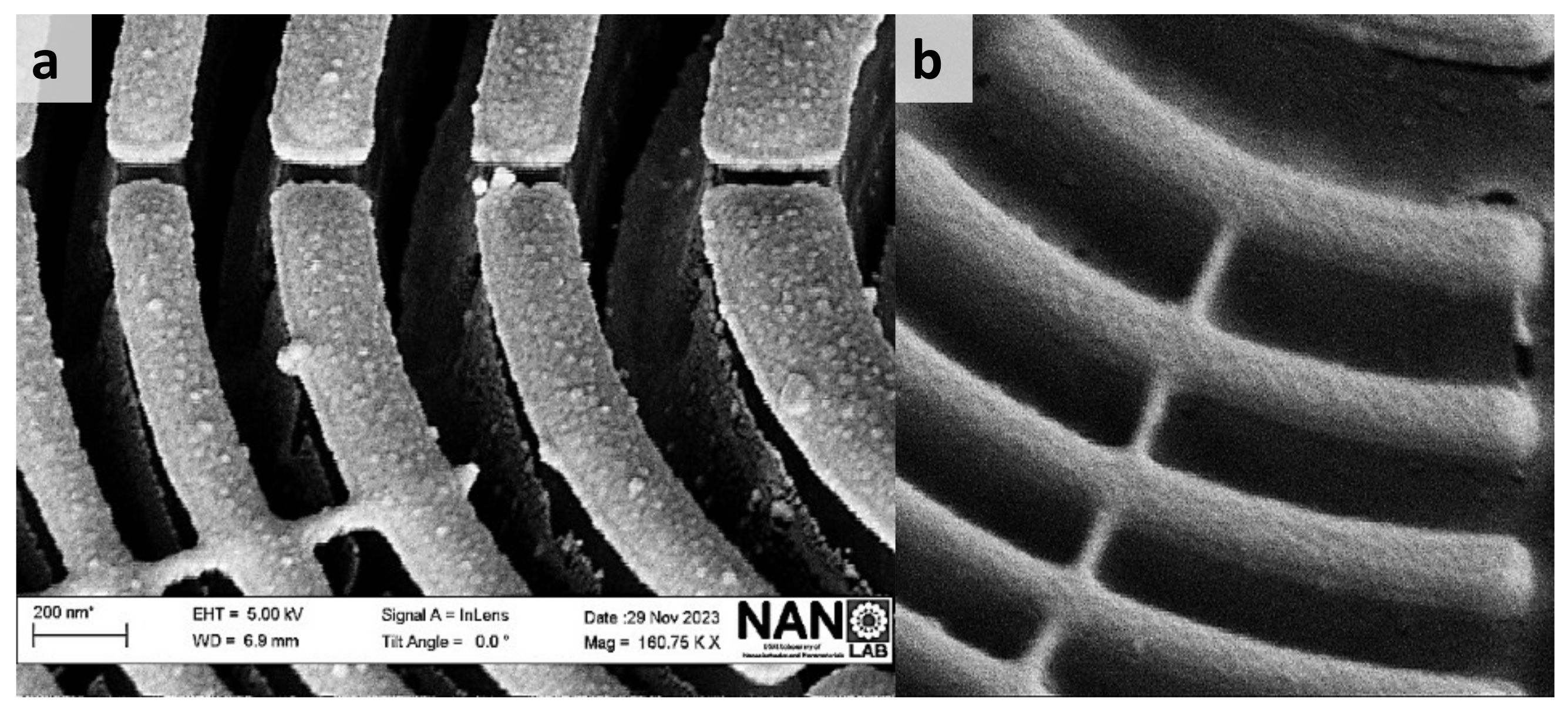
2.3. Silicon Cryogenic Etching
3. Conclusions
Author Contributions
Funding
Data Availability Statement
Conflicts of Interest
Correction Statement
Appendix A. Final Computer-Aided Designs (CAD)
Appendix B. Etching
Appendix B.1. Etching Recipes

| Parameter | Recipe 1 | Recipe 2 | Recipe 3 | Recipe 4 |
|---|---|---|---|---|
| Pressure (mTorr) | 5 | 100 | 12 | 6.5 |
| Rf power (W) | 30 | 50 | 10 | 8 |
| ICP power (W) | 500 | 0 | 1200 | 600 |
| Cl2 flow (sccm) | 20 | 17.2 | 45 | 44 |
| O2 flow (sccm) | 20 | 4 | 5 | 6 |
| Temperature (°C) | 10 | 19 | 50 | 15 |
| Parameter | Recipe 1 | Recipe 2 | Recipe 3 |
|---|---|---|---|
| Pressure (mTorr) | 10 | 10 | 10 |
| Rf power (W) | 4 | 4 | 4 |
| ICP power (W) | 1000 | 1000 | 1000 |
| SF6 flow (sccm) | 60 | 60 | 60 |
| O2 flow (sccm) | 10 | 12 | 18 |
| Temperature (°C) | −110 | −120 | −120 |
Appendix B.2. Silicon Etching Without Chromium Mask
Appendix B.3. Under-Etching
Appendix B.4. Over-Etching
Appendix B.5. Etching Rate
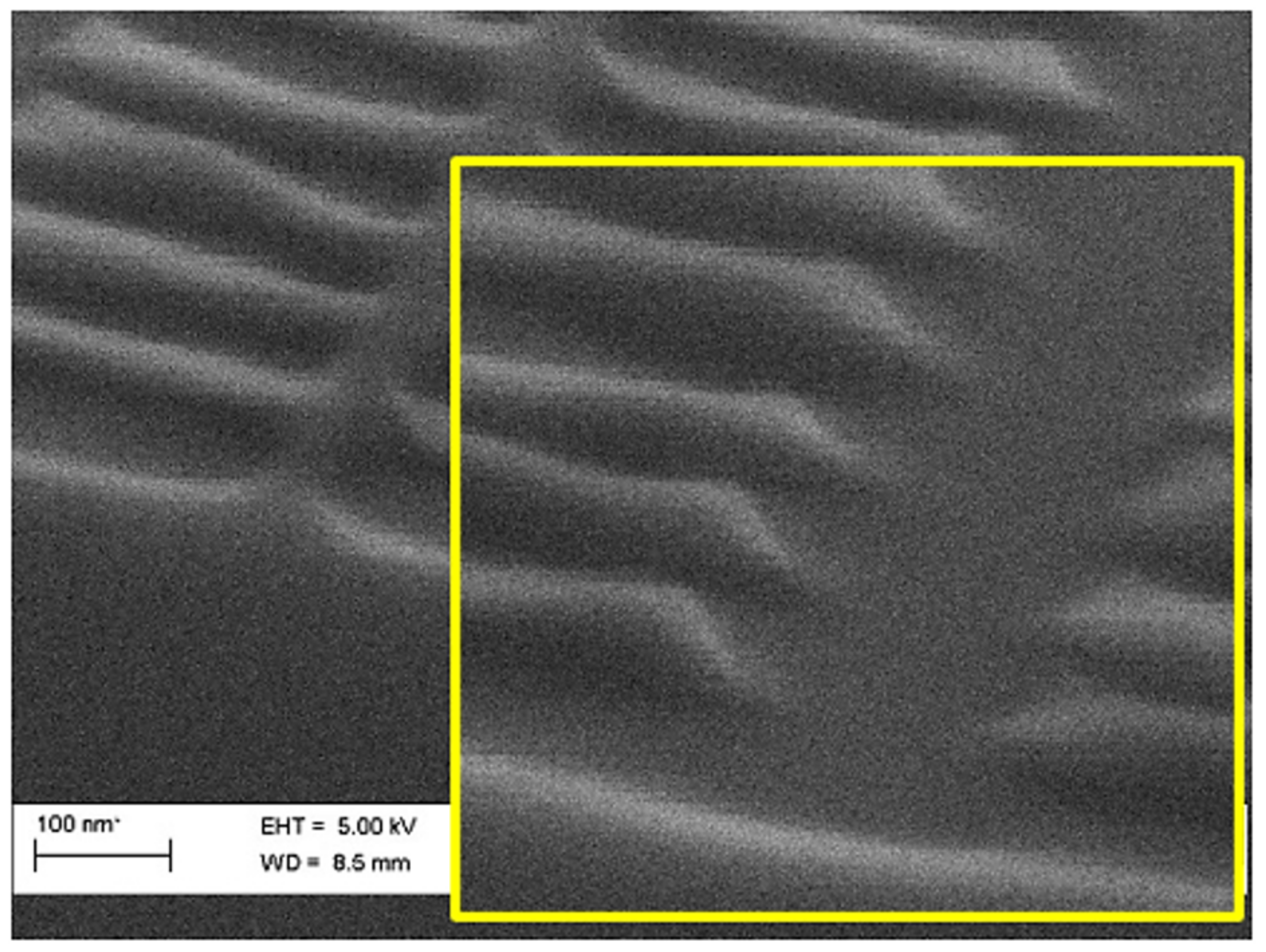
Appendix B.6. Etching Profiles

Appendix C. Fresnel Zone Plate Parameters
| Parameter | Notation | Values |
|---|---|---|
| Radiation wavelength | 1.03 nm (1.2 keV) | |
| Outer zone width | 50 nm | |
| Number of zones | N | 100 |
| Focal length | 970.87 µm | |
| Diameter | 20 µm | |
| Numerical Aperture (1st order) | NA = | 0.0103 |
| Spatial Resolution (1st order) | 61 nm |
References
- Clericò, V.; Amado, M.; Díez, E. Electron beam lithography and its use on 2D materials. In Nanofabrication: Nanolithography Techniques and Their Applications; De Teresa, J.M., Ed.; IOP Publishing: Bristol, UK, 2020; pp. 1–49. [Google Scholar] [CrossRef]
- Dyson, N.A. X-Rays in Atomic and Nuclear Physics; Cambridge University Press: Cambridge, UK, 1990. [Google Scholar] [CrossRef]
- Zhang, F. Application of machine learning in CT images and X-rays of COVID-19 pneumonia. Medicine 2021, 100, e26855. [Google Scholar] [CrossRef] [PubMed]
- Vourlias, G. Application of X-ray diffraction for identifying thin oxide surface layers on zinc coatings. Coatings 2020, 10, 1005. [Google Scholar] [CrossRef]
- Llovet, X.; Moy, A.; Pinard, P.T.; Fournelle, J.H. Reprint of: Electron probe microanalysis: A review of recent developments and applications in materials science and engineering. Prog. Mater. Sci. 2021, 120, 100818. [Google Scholar] [CrossRef]
- Donnelly, C.; Scagnoli, V. Imaging three-dimensional magnetic systems with X-rays. J. Phys. Condens. Matter 2020, 32, 213001. [Google Scholar] [CrossRef]
- Rosenzweig, J.B.; Majernik, N.; Robles, R.R.; Andonian, G.; Camacho, O.; Fukasawa, A.; Kogar, A.; Lawler, G.; Miao, J.; Musumeci, P.; et al. An ultra-compact X-ray free-electron laser. New J. Phys. 2020, 22, 093067. [Google Scholar] [CrossRef]
- Huang, N.; Deng, H.; Liu, B.; Wang, D.; Zhao, Z. Features and futures of X-ray free-electron lasers. Innovation 2021, 2, 100097. [Google Scholar] [CrossRef]
- Decking, W.; Abeghyan, S.; Abramian, P.; Abramsky, A.; Aguirre, A.; Albrecht, C.; Alou, P.; Altarelli, M.; Altmann, P.; Amyan, K.; et al. A MHz-repetition-rate hard X-ray free-electron laser driven by a superconducting linear accelerator. Nat. Photonics 2020, 14, 391–397. [Google Scholar] [CrossRef]
- Prat, E.; Abela, R.; Aiba, M.; Alarcon, A.; Alex, J.; Arbelo, Y.; Arrell, C.; Arsov, V.; Bacellar, C.; Beard, C.; et al. A compact and cost-effective hard X-ray free-electron laser driven by a high-brightness and low-energy electron beam. Nat. Photonics 2020, 14, 748–754. [Google Scholar] [CrossRef]
- Fajardo, P.; Erdinger, F.; Fischer, P.; Ruat, M.; Schimansky, D. Digital integration: A novel readout concept for XIDER, an X-ray detector for the next generation of synchrotron radiation sources. J. Instrum. 2020, 15, C01040. [Google Scholar] [CrossRef]
- Baranov, G.; Bogomyagkov, A.; Morozov, I.; Sinyatkin, S.; Levichev, E. Lattice optimization of a fourth-generation synchrotron radiation light source in Novosibirsk. Phys. Rev. Accel. Beams 2021, 24, 120704. [Google Scholar] [CrossRef]
- Smaluk, V.; Shaftan, T. Electron beam emittance at operational intensity in fourth-generation synchrotron light sources. arXiv 2024, arXiv:2402.05204. [Google Scholar] [CrossRef]
- Symes, D.R.; Cole, J.M.; Wood, J.C.; Mangles, S.P.D.; Najmudin, Z. Comparison of the Properties of Laser-Driven X-Ray Sources to Existing Compact X-Ray Sources. unpublished.
- Barbrel, B.; Barjou, E.; Courjaud, A.; Dorchies, F.; Lehoux, P.; Mastropietro, F.; Song, P.; Bakkali, A. Demonstration of a robust laser-driven X-ray source for CT. In Proceedings of the 13th Conference on Industrial Computed Tomography (iCT) 2023, Wels, Austria, 6–9 February 2024. [Google Scholar] [CrossRef]
- Zeraouli, G. Experimental Studies for Generation, Transport and Applications of Ultra-Fast Laser Driven X-Ray Sources. 2020; unpublished. [Google Scholar]
- Brzhezinskaya, M.; Firsov, A.; Holldack, K.; Kachel, T.; Mitzner, R.; Pontius, N.; Schmidt, J.-S.; Sperling, M.; Stamm, C.; Föhlich, A.; et al. A novel monochromator for experiments with ultrashort X-ray pulses. J. Synchrotron Radiat. 2013, 20, 522–530. [Google Scholar] [CrossRef] [PubMed]
- Kroll, T.; Kern, J.; Kubin, M.; Ratner, D.; Gul, S.; Fuller, F.D.; Löchel, H.; Krzywinski, J.; Lutman, A.; Ding, Y.; et al. X-ray absorption spectroscopy using a self-seeded soft X-ray free-electron laser. Opt. Express 2016, 24, 22469–22480. [Google Scholar] [CrossRef] [PubMed]
- Li, X.; Cai, X.; Liu, C.; Kim, Y.; Badloe, T.; Liu, H.; Rho, J.; Xiao, S. Cascaded metasurfaces enabling adaptive aberration corrections for focus scanning. Opto-Electron. Adv. 2024, 7, 240085. [Google Scholar] [CrossRef]
- Cui, M.; Xiong, S.; Yang, N.; Wang, Y.; Wang, Z.; Luo, M.; Yao, C.; Deguchi, Y. Applications of laser-induced breakdown spectroscopy in industrial measurement and monitoring: Multi-technology combination. Appl. Spectrosc. Rev. 2024, 1–49. [Google Scholar] [CrossRef]
- Ekman, A.; Chen, J.-H.; Vanslembrouck, B.; Loconte, V.; Larabell, C.A.; Le Gros, M.A.; Weinhardt, V. Extending Imaging Volume in Soft X-ray Tomography. Adv. Photonics Res. 2023, 4, 2200142. [Google Scholar] [CrossRef]
- Tong, X.; Chen, Y.; Xu, Z.; Li, Y.; Xing, Z.; Mu, C.; Zhao, J.; Zhen, X.; Mao, C.; Tai, R. High-efficiency focusing and imaging by dielectric kinoform zone plate lenses with soft X-rays. J. Synchrotron Radiat. 2023, 30, 319–326. [Google Scholar] [CrossRef]
- Zhu, J.; Chen, Y.; Xie, S.; Zhang, L.; Wang, C.; Tai, R. Nanofabrication of 30 nm Au zone plates by e-beam lithography and pulse voltage electroplating for soft X-ray imaging. Microelectron. Eng. 2020, 225, 111254. [Google Scholar] [CrossRef]
- DiFabrizio, E.; Romanato, F.; Gentili, M.; Cabrini, S.; Kaulich, B.; Susini, J.; Barrett, R. High-efficiency multilevel zone plates for keV X-rays. Nature 1999, 401, 895–898. [Google Scholar] [CrossRef]
- Rogers, E.T.F.; Lindberg, J.; Roy, T.; Savo, S.; Chad, J.E.; Dennis, M.R.; Zheludev, N.I. A super-oscillatory lens optical microscope for subwavelength imaging. Nat. Mater. 2012, 11, 432–435. [Google Scholar] [CrossRef]
- Kong, X.-T.; Khan, A.A.; Kidambi, P.R.; Deng, S.; Yetisen, A.K.; Dlubak, B.; Hiralal, P.; Montelongo, Y.; Bowen, J.; Xavier, S.; et al. Graphene-based ultrathin flat lenses. ACS Photonics 2015, 2, 200–207. [Google Scholar] [CrossRef]
- Li, X.; Wei, L.; Poelma, R.H.; Vollebregt, S.; Wei, J.; Urbach, H.P.; Sarro, P.M.; Zhang, G.Q. Stretchable binary Fresnel lens for focus tuning. Sci. Rep. 2016, 6, 25348. [Google Scholar] [CrossRef] [PubMed]
- Zheng, X.; Jia, B.; Lin, H.; Qiu, L.; Li, D.; Gu, M. Highly efficient and ultra-broadband graphene oxide ultrathin lenses with three-dimensional subwavelength focusing. Nat. Commun. 2015, 6, 8433. [Google Scholar] [CrossRef] [PubMed]
- Low, M.J.; Lee, H.; Lim, C.H.J.; Sandeep, C.S.; Murukeshan, V.M.; Kim, S.-W.; Kim, Y.-J. Laser-induced reduced-graphene-oxide micro-optics patterned by femtosecond laser direct writing. Appl. Surf. Sci. 2020, 526, 146647. [Google Scholar] [CrossRef]
- Virgilli, E.; Halloin, H.; Skinner, G. Laue and Fresnel lenses. In Handbook of X-Ray and Gamma-Ray Astrophysics; Springer: Berlin/Heidelberg, Germany, 2024; pp. 1671–1709. [Google Scholar] [CrossRef]
- Davis, A.; Kühnlenz, F. Optical design using Fresnel lenses: Basic principles and some practical examples. Opt. Photonik 2007, 2, 52–55. [Google Scholar] [CrossRef]
- Attwood, D. Soft X-Rays and Extreme Ultraviolet Radiation: Principles and Applications; Cambridge University Press: Cambridge, UK, 2000. [Google Scholar] [CrossRef]
- Kawazoe, T.; Takahashi, T.; Ohtsu, M. Evaluation of the dynamic range and spatial resolution of nonadiabatic optical near-field lithography through fabrication of Fresnel zone plates. Appl. Phys. B 2010, 98, 5–11. [Google Scholar] [CrossRef]
- Li, Y.; Lu, W.; Wang, S.; Yuan, Q.; Kong, X.; Han, L.; Xia, Y. Fabrication of multilayer Fresnel zone plate for hard X-ray microscopy by atomic layer deposition and focused ion beam milling. Vacuum 2023, 209, 111776. [Google Scholar] [CrossRef]
- Mayer, M.; Keskinbora, K.; Grévent, C.; Szeghalmi, A.; Knez, M.; Weigand, M.; Snigirev, A.; Snigireva, I.; Schütz, G. Efficient focusing of 8 keV X-rays with multilayer Fresnel zone plates fabricated by atomic layer deposition and focused ion beam milling. J. Synchrotron Radiat. 2013, 20, 433–440. [Google Scholar] [CrossRef]
- Sarkar, S.S.; Solak, H.H.; Raabe, J.; David, C.; van der Veen, J.F. Fabrication of Fresnel zone plates with 25 nm zone width using extreme ultraviolet holography. Microelectron. Eng. 2010, 87, 854–858. [Google Scholar] [CrossRef]
- Okabe, T.; Utsumi, K.; Ogino, K.; Shinonaga, Y.; Miyatake, M.; Yoshimoto, S.; Taniguchi, J.; Sasaki, S. Electron beam mastering system using a vacuum-compatible hydrodynamic spindle. Microelectron. Eng. 2015, 142, 64–69. [Google Scholar] [CrossRef]
- Mohammad, M.A.; Muhammad, M.; Dew, S.K.; Stepanova, M. Fundamentals of electron beam exposure and development. In Nanofabrication: Techniques and Principles; Springer: Berlin/Heidelberg, Germany, 2011; pp. 11–41. [Google Scholar] [CrossRef]
- Brault, R.G.; Kubena, R.L.; Metzger, R.A. Bilevel polysiloxane resist for ion-beam and electron-beam lithography. In Advances in Resist Technology and Processing II; SPIE: Bellingham, WA, USA, 1985; Volume 539, pp. 70–73. [Google Scholar] [CrossRef]
- Lyons, A.; Hartley, J. Proximity effect correction parameters for patterning of EUV reticles with Gaussian electron-beam lithography. In Photomask Technology 2012; SPIE: Bellingham, WA, USA, 2012; Volume 8522, pp. 715–724. [Google Scholar] [CrossRef]
- Zhao, G.; Li, Y. A comparison study of tantalum-nitrogen and chromium absorber in extreme ultraviolet mask fabrication using electron-beam lithography simulation. In Photomask and Next-Generation Lithography Mask Technology XIV; SPIE: Bellingham, WA, USA, 2007; Volume 6607, pp. 915–922. [Google Scholar] [CrossRef]
- Hossain, M.N.; Justice, J.; Lovera, P.; McCarthy, B.; O’Riordan, A.; Corbett, B. High aspect ratio nano-fabrication of photonic crystal structures on glass wafers using chrome as hard mask. Nanotechnology 2014, 25, 355301. [Google Scholar] [CrossRef] [PubMed]
- Parfeniukas, K.; Rahomäki, J.; Giakoumidis, S.; Seiboth, F.; Wittwer, F.; Schroer, C.G.; Vogt, U. Improved tungsten nanofabrication for hard X-ray zone plates. Microelectron. Eng. 2016, 152, 6–9. [Google Scholar] [CrossRef]
- Liu, Z.; Wu, Y.; Harteneck, B.; Olynick, D. Super-selective cryogenic etching for sub-10 nm features. Nanotechnology 2012, 24, 015305. [Google Scholar] [CrossRef]
- David, C.; Gorelick, S.; Rutishauser, S.; Krzywinski, J.; Vila-Comamala, J.; Guzenko, V.A.; Bunk, O.; Färm, E.; Ritala, M.; Cammarata, M.; et al. Nanofocusing of hard X-ray free electron laser pulses using diamond based Fresnel zone plates. Sci. Rep. 2011, 1, 57. [Google Scholar] [CrossRef]
- Reisinger, T.; Eder, S.; Greve, M.M.; Smith, H.I.; Holst, B. Free-standing silicon-nitride zone plates for neutral-helium microscopy. Microelectron. Eng. 2010, 87, 1011–1014. [Google Scholar] [CrossRef]
- Born, M.; Wolf, E. Principles of Optics: Electromagnetic Theory of Propagation, Interference and Diffraction of Light. Phys. Today 2000, 53, 77–78. [Google Scholar] [CrossRef]
- Chang, T.H.P. Proximity effect in electron-beam lithography. J. Vac. Sci. Technol. 1975, 12, 1271–1275. [Google Scholar] [CrossRef]
- van de Kraats, A.; Murali, R. Proximity Effect in E-Beam Lithography; Nanotechnology Research Center, Georgia Institute of Technology: Atlanta, GA, USA, 2005. [Google Scholar]
- De Teresa, J.M. Nanofabrication: Nanolithography Techniques and Their Applications; IOP Publishing: Bristol, UK, 2020. [Google Scholar] [CrossRef]
- Chen, Y.; Huang, Z.; Chen, X.; Chen, J.; Zhu, W. Proximity Effect Aware Detailed Placement in Electron Beam Lithography. MATEC Web Conf. 2018, 232, 04046. [Google Scholar] [CrossRef]
- Sundaram, V.M.; Wen, S.B. An easy method to perform e-beam negative tone lift-off fabrication on dielectric material with a sandwiched conducting polymer layer. J. Micromech. Microeng. 2011, 21, 065021. [Google Scholar] [CrossRef]
- Munkhbat, B.; Küçüköz, B.; Baranov, D.G.; Antosiewicz, T.J.; Shegai, T.O. Nanostructured transition metal dichalcogenide multilayers for advanced nanophotonics. Laser Photonics Rev. 2023, 17, 2200057. [Google Scholar] [CrossRef]
- Muhammad, M.; Buswell, S.C.; Dew, S.K.; Stepanova, M. Nanopatterning of PMMA on insulating surfaces with various anticharging schemes using 30 keV electron beam lithography. J. Vac. Sci. Technol. B Microelectron. Nanometer Struct. Process. Meas. Phenom. 2011, 29, 06FJ01. [Google Scholar] [CrossRef]
- Demers, H.; Poirier-Demers, N.; Phillips, M.R.; de Jonge, N.; Drouin, D. Three-dimensional electron energy deposition modeling of cathodoluminescence emission near threading dislocations in GaN and electron-beam lithography exposure parameters for a PMMA resist. Microsc. Microanal. 2012, 18, 1220–1228. [Google Scholar] [CrossRef] [PubMed]
- Hoffman, D.W.; Thornton, J.A. Internal Stresses in Cr, Mo, Ta, and Pt Films Deposited by Sputtering from a Planar Magnetron Source. J. Vac. Sci. Technol. 1982, 20, 355–358. [Google Scholar] [CrossRef]
- Bîrjega, M.I.; Popescu-Pogrion, N.; Sârbu, C.; Topa, V. Particularities in the Growth Behaviour of Vacuum-Evaporated Chromium Thin Films. Thin Solid Film. 1979, 58, 217–221. [Google Scholar] [CrossRef]
- Staaks, D.; Yu, Z.; Dhuey, S.D.; Sassolini, S.; Lee, K.Y.; Rangelow, I.W.; Olynick, D.L. Temperature and Oxygen Concentration Effects on Anisotropy in Chromium Hard Mask Etching for Nanoscale Fabrication. J. Vac. Sci. Technol. A 2019, 37, 061306. [Google Scholar] [CrossRef]
- Scholten, K.; Meng, E. Electron-beam lithography for polymer bioMEMS with submicron features. Microsyst. Nanoeng. 2016, 2, 16053. [Google Scholar] [CrossRef]
- Gorelick, S.; Guzenko, V.A.; Vila-Comamala, J.; David, C. Direct e-beam writing of dense and high aspect ratio nanostructures in thick layers of PMMA for electroplating. Nanotechnology 2010, 21, 295303. [Google Scholar] [CrossRef]
- Tiwari, C.S.; Lim, Y.S.; Fulton, R.; Srinivasan, J.; Gisinger, M.; Flynn, P.; Mak, L.H. Characterization of the Descum Process for Various Silicon Substrates Doping. ECS Trans. 2013, 58, 251. [Google Scholar] [CrossRef]
- Racka-Szmidt, K.; Stonio, B.; Żelazko, J.; Filipiak, M.; Sochacki, M. A review: Inductively coupled plasma reactive ion etching of silicon carbide. Materials 2021, 15, 123. [Google Scholar] [CrossRef]
- Defforge, T.; Song, X.; Gautier, G.; Tillocher, T.; Dussart, R.; Kouassi, S.; Tran-Van, F. Scalloping removal on DRIE via using low concentrated alkaline solutions at low temperature. Sens. Actuators A Phys. 2011, 170, 114–120. [Google Scholar] [CrossRef]
- Cadarso, V.J.; Chidambaram, N.; Jacot-Descombes, L.; Schift, H. High-aspect-ratio nanoimprint process chains. Microsyst. Nanoeng. 2017, 3, 17017. [Google Scholar] [CrossRef] [PubMed]
- Clericò, V.; Delgado-Notario, J.A.; Saiz-Bretín, M.; Malyshev, A.V.; Meziani, Y.M.; Hidalgo, P.; Méndez, B.; Amado, M.; Domínguez-Adame, F.; Diez, E. Quantum nanoconstrictions fabricated by cryo-etching in encapsulated graphene. Sci. Rep. 2019, 9, 13572. [Google Scholar] [CrossRef] [PubMed]
- Sökmen, Ü.; Stranz, A.; Fündling, S.; Merzsch, S.; Neumann, R.; Wehmann, H.-H.; Peiner, E.; Waag, A. Shallow and deep dry etching of silicon using ICP cryogenic reactive ion etching process. Microsyst. Technol. 2010, 16, 863–870. [Google Scholar] [CrossRef]
- Vugts, M.J.M.; Hermans, L.J.F.; Beijerinck, H.C.W. Ion-assisted Si/XeF2 etching: Temperature dependence in the range 100–1000 K. J. Vac. Sci. Technol. A Vac. Surfaces Film. 1996, 14, 2820–2826. [Google Scholar] [CrossRef]
- Aachboun, S.; Ranson, P.; Hilbert, C.; Boufnichel, M. Cryogenic etching of deep narrow trenches in silicon. J. Vac. Sci. Technol. A Vac. Surfaces Film. 2000, 18, 1848–1852. [Google Scholar] [CrossRef]
- Keskinbora, K.; Grévent, C.; Bechtel, M.; Weigand, M.; Goering, E.; Nadzeyka, A.; Peto, L.; Rehbein, S.; Schneider, G.; Follath, R.; et al. Ion Beam Lithography for Fresnel Zone Plates in X-ray Microscopy. Opt. Express 2013, 21, 11747–11756. [Google Scholar] [CrossRef]
- Uhlén, F.; Nilsson, D.; Rahomäki, J.; Belova, L.; Schroer, C.G.; Seiboth, F.; Holmberg, A.; Hertz, H.M.; Vogt, U. Nanofabrication of tungsten zone plates with integrated platinum central stop for hard X-ray applications. Microelectron. Eng. 2014, 116, 40–43. [Google Scholar] [CrossRef]
- Di Fabrizio, E.; Gentili, M.; Grella, L.; Baciocchi, M.; Krasnoperova, A.; Cerrina, F.; Yun, W.; Lai, B.; Gluskin, E. High-performance multilevel blazed X-ray microscopy Fresnel zone plates: Fabricated using X-ray lithography. J. Vac. Sci. Technol. B Microelectron. Nanometer Struct. Process. Meas. Phenom. 1994, 12, 3979–3985. [Google Scholar] [CrossRef]
- Braun, H.-G. Electron Beam Lithography; Leibniz-Institut für Polymerforschung Dresden: Dresden, Germany, 2008. [Google Scholar]
- RiusSuñé, G. Electron Beam Lithography for Nanofabrication; Universitat Autònoma de Barcelona: Bellaterra, Spain, 2008. [Google Scholar]
- Nguyen, V.T.H.; Shkondin, E.; Jensen, F.; Hübner, J.; Leussink, P.; Jansen, H. Ultrahigh aspect ratio etching of silicon in SF6-O2 plasma: The clear-oxidize-remove-etch (CORE) sequence and chromium mask. J. Vac. Sci. Technol. A 2020, 38, 053002. [Google Scholar] [CrossRef]
- Tinck, S.; Tillocher, T.; Georgieva, V.; Dussart, R.; Neyts, E.; Bogaerts, A. Concurrent effects of wafer temperature and oxygen fraction on cryogenic silicon etching with SF6/O2 plasmas. Plasma Process. Polym. 2017, 14, 1700018. [Google Scholar] [CrossRef]
- De Boer, M.J.; Gardeniers, J.G.E.; Jansen, H.V.; Smulders, E.; Gilde, M.-J.; Roelofs, G.; Sasserath, J.N.; Elwenspoek, M. Guidelines for etching silicon MEMS structures using fluorine high-density plasmas at cryogenic temperatures. J. Microelectromech. Syst. 2002, 11, 385–401. [Google Scholar] [CrossRef]
- Marcos, G.; Rhallabi, A.; Ranson, P. Topographic and kinetic effects of the SF6/O2 rate during a cryogenic etching process of silicon. J. Vac. Sci. Technol. B Microelectron. Nanometer Struct. Process. Meas. Phenom. 2004, 22, 1912–1922. [Google Scholar] [CrossRef]
- Gomez, S.; JunBelen, R.; Kiehlbauch, M.; Aydil, E.S. Etching of high aspect ratio structures in Si using SF6/O2 plasma. J. Vac. Sci. Technol. A Vac. Surfaces Film. 2004, 22, 606–615. [Google Scholar] [CrossRef]
- Rahman, F.; Carbaugh, D.J.; Wright, J.T.; Rajan, P.; Pandya, S.G.; Kaya, S. A review of polymethyl methacrylate (PMMA) as a versatile lithographic resist—With emphasis on UV exposure. Microelectron. Eng. 2020, 224, 111238. [Google Scholar] [CrossRef]
- Ilie, M.; Marculescu, B.; Moldovan, N.; Nastase, N.; Olteanu, M. Adhesion between PMMA mask layer and silicon wafer in KOH aqueous solution. Mater. Device Charact. Micromach. 1998, 3512, 422–430. [Google Scholar] [CrossRef]
- Hoang Nguyen, V.T.H.; Jensen, F.; Hübner, J.; Shkondin, E.; Cork, R.; Ma, K.; Leussink, P.; DeMalsche, W.; Jansen, H. Cr and CrOx etching using SF6 and O2 plasma. J. Vac. Sci. Technol. 2021, 39, 032201. [Google Scholar] [CrossRef]
- Dey, R.K.; Ekinci, H.; Cui, B. Effects of mask material conductivity on lateral undercut etching in silicon nano-pillar fabrication. J. Vac. Sci. Technol. 2020, 38, 012207. [Google Scholar] [CrossRef]
- Wu, Y.; Olynick, D.L.; Goodyear, A.; Peroz, C.; Dhuey, S.; Liang, X.; Cabrini, S. Cryogenic etching of nano-scale silicon trenches with resist masks. Microelectron. Eng. 2011, 88, 2785–2789. [Google Scholar] [CrossRef]
- Boufnichel, M.; Lefaucheux, P.; Aachboun, S.; Dussart, R.; Ranson, P. Origin, control and elimination of undercut in silicon deep plasma etching in the cryogenic process. Microelectron. Eng. 2005, 77, 327–336. [Google Scholar] [CrossRef]
- Addae-Mensah, K.A.; Retterer, S.; Opalenik, S.R.; Thomas, D.; Lavrik, N.V.; Wikswo, J.P. Cryogenic etching of silicon: An alternative method for fabrication of vertical microcantilever master molds. J. Microelectromech. Syst. 2009, 19, 64–74. [Google Scholar] [CrossRef]
- Kamto Tegueu, A.M. Fabrication and Reliability Testing of Copper-Filled Through-Silicon Vias for Three-Dimensional Chip stacking Applications. Ph.D. Dissertation, University of Alabama Libraries, Tuscaloosa, AL, USA, 2010. Available online: https://ir.ua.edu/handle/123456789/1014 (accessed on 12 September 2024).
- Campo, A.; Cardinaud, C.; Turban, G. Investigation of Si and Ge etching mechanisms in radiofrequency CF2-O2 plasma based on surface reactivities. Plasma Sources Sci. Technol. 1995, 4, 398. [Google Scholar] [CrossRef]
- Oehrlein, G.S.; Robey, S.W.; Lindström, J.L. Surface processes in CF4/O2 reactive etching of silicon. Appl. Phys. Lett. 1988, 52, 1170–1172. [Google Scholar] [CrossRef]
- Ninomiya, K.; Suzuki, K.; Nishimatsu, S.; Okada, O. Role of sulfur atoms in microwave plasma etching of silicon. J. Appl. Phys. 1987, 62, 1459–1468. [Google Scholar] [CrossRef]


| E-Beam Lithography Parameters | |
|---|---|
| Substrate | Si chip 1 cm × 1 cm |
| Resist | PMMA 2% |
| Resist thickness | 87 nm |
| Electron beam current | 0.016114 nA |
| Electron beam energy | 15 keV |
| Step size | 2 nm |
| Dwelltime | 0.000284 ms |
| Column aperture | 7.5 µm |
| Z stage position | 17 mm |
| Working distance | 5 mm |
| Exposure field | 100 µm × 100 µm |
| Magnification | 1500 |
| Silicon Reactive Ion Etching | |
|---|---|
| Pressure | 10 mTorr |
| Rf power | 4 W |
| ICP power | 1000 W |
| SF6 flow | 60 sccm |
| O2 flow | 8 sccm |
| Temperature | −110 °C |
| Time | 15 s |
| etching rate | 2.63 µm/nm |
| Silicon Reactive Ion Etching | |
|---|---|
| Pressure | 10 mTorr |
| Rf power | 4 W |
| ICP power | 1000 W |
| SF6 flow | 60 sccm |
| O2 flow | 15 sccm |
| Temperature | −120 °C |
| Time | 2 mn |
| etching rate | 2.25 µm/nm |
Disclaimer/Publisher’s Note: The statements, opinions and data contained in all publications are solely those of the individual author(s) and contributor(s) and not of MDPI and/or the editor(s). MDPI and/or the editor(s) disclaim responsibility for any injury to people or property resulting from any ideas, methods, instructions or products referred to in the content. |
© 2024 by the authors. Licensee MDPI, Basel, Switzerland. This article is an open access article distributed under the terms and conditions of the Creative Commons Attribution (CC BY) license (https://creativecommons.org/licenses/by/4.0/).
Share and Cite
Labani, M.; Clericò, V.; Diez, E.; Gatti, G.; Amado, M.; Pérez-Rodríguez, A. Optimization of Soft X-Ray Fresnel Zone Plate Fabrication Through Joint Electron Beam Lithography and Cryo-Etching Techniques. Nanomaterials 2024, 14, 1898. https://doi.org/10.3390/nano14231898
Labani M, Clericò V, Diez E, Gatti G, Amado M, Pérez-Rodríguez A. Optimization of Soft X-Ray Fresnel Zone Plate Fabrication Through Joint Electron Beam Lithography and Cryo-Etching Techniques. Nanomaterials. 2024; 14(23):1898. https://doi.org/10.3390/nano14231898
Chicago/Turabian StyleLabani, Maha, Vito Clericò, Enrique Diez, Giancarlo Gatti, Mario Amado, and Ana Pérez-Rodríguez. 2024. "Optimization of Soft X-Ray Fresnel Zone Plate Fabrication Through Joint Electron Beam Lithography and Cryo-Etching Techniques" Nanomaterials 14, no. 23: 1898. https://doi.org/10.3390/nano14231898
APA StyleLabani, M., Clericò, V., Diez, E., Gatti, G., Amado, M., & Pérez-Rodríguez, A. (2024). Optimization of Soft X-Ray Fresnel Zone Plate Fabrication Through Joint Electron Beam Lithography and Cryo-Etching Techniques. Nanomaterials, 14(23), 1898. https://doi.org/10.3390/nano14231898