Communication

Effect of Temperature-Dependent Low Oxygen Partial Pressure Annealing on SiC MOS

1
High-Frequency High-Voltage Device and Integrated Circuits R&D Center, Institute of Microelectronics of the Chinese Academy of Sciences, Beijing 100029, China
2
University of Chinese Academy of Sciences, Beijing 100049, China
*
Authors to whom correspondence should be addressed.
Nanomaterials 2024, 14(2), 192; https://doi.org/10.3390/nano14020192
Submission received: 14 December 2023 / Revised: 10 January 2024 / Accepted: 12 January 2024 / Published: 15 January 2024

Abstract

:
Oxygen post annealing is a promising method for improving the quality of the SiC metal oxide semiconductor (MOS) interface without the introduction of foreign atoms. In addition, a low oxygen partial pressure annealing atmosphere would prevent the additional oxidation of SiC, inhibiting the generation of new defects. This work focuses on the effect and mechanism of low oxygen partial pressure annealing at different temperatures (900–1250 °C) in the SiO2/SiC stack. N2 was used as a protective gas to achieve the low oxygen partial pressure annealing atmosphere. X-ray photoelectron spectroscopy (XPS) characterization was carried out to confirm that there are no N atoms at or near the interface. Based on the reduction in interface trap density (Dit) and border trap density (Nbt), low oxygen partial pressure annealing is proven to be an effective method in improving the interface quality. Vacuum annealing results and time of flight secondary ion mass spectrometry (ToF-SIMS) results reveal that the oxygen vacancy (V[O]) filling near the interface is the dominant annealing mechanism. The V[O] near the interface is filled more by O2 in the annealing atmosphere with the increase in temperature.

1. Introduction

Silicon carbide (SiC) has been attracting wide attention because of its excellent physical properties, such as wide bandgap, high thermal conductivity, and high breakdown field [1,2,3]. On this basis, SiC metal oxide semiconductor field effect transistors (MOSFETs) are also promising power devices with low loss and fast switching [3,4,5]. However, the interface state density (Dit) near the SiC conduction band edge (EC) of SiC MOSFETs is more than an order of magnitude higher than that of Si MOSFETs. Consequently, the electrical characteristics of the SiC MOSFETs are limited by the existence of the high Dit, which could be attributed to the generation of C defects in the SiC oxidation process [6,7,8].
Many studies have shown that the Dit of the SiO2/SiC stack can be reduced by optimizing the oxidation and post oxidation annealing (POA) processes. For example, the oxidation of the deposited Si on the SiC layer instead of direct oxidation of SiC can minimize the carbon-related defects in the oxide layer [9]. In addition, high-pressure microwave plasma oxidation is designed to promote a more complete interface oxidation reaction using atomic oxygen species [10]. Meanwhile, POA in different atmospheres for SiC MOS capacitors, such as POCl3 [11], N2 [12], NO [13], N2O [14], etc., are proposed. The key to these annealing methods is to introduce foreign passivating atoms into the SiO2/SiC stacks to passivate the interface. For example, N atoms can passivate the C-related defects at the interface mainly by replacing some C atoms to form stable Si-N bonds [15,16]. However, the passivation atoms may induce fast states or hole traps [17], which can lead to reliability problems. Therefore, oxygen is an alternative atmosphere in the POA process. We have reported that the O2 POA can improve the quality of the SiC MOS without introducing any foreign atoms. The deconvolution analysis of X-ray photoelectron spectroscopy (XPS) of Si 2p spectra at different distances from the interface reveals that O atoms fill the oxygen vacancy at and near the interface [18]. In order to avoid further oxidation of SiC induced by excess oxygen during the annealing process, a relatively low oxygen partial pressure should be selected [19]. Considering the oxygen vacancy filling process, the effect of annealing at low oxygen partial pressure is highly dependent on the temperature. T. Kobayashi et al. reported that low oxygen partial pressure annealing at high temperature (≥1300 °C) can reduce the Dit value and prevent oxide layer degradation [19]. However, few studies have pointed out the annealing effect of low oxygen partial pressure at temperatures below 1300 °C.
In this paper, we focus on the temperature range from 900 to 1250 °C to study the effect of temperature on low oxygen partial pressure annealing. The N2 is utilized as a protective gas to achieve an annealing atmosphere with a low oxygen partial pressure. Electrical characteristics were measured to analyze the annealing effect, and the mechanism of the corresponding temperature range was revealed by the time of flight secondary ion mass spectrometry (ToF-SIMS) characterization.

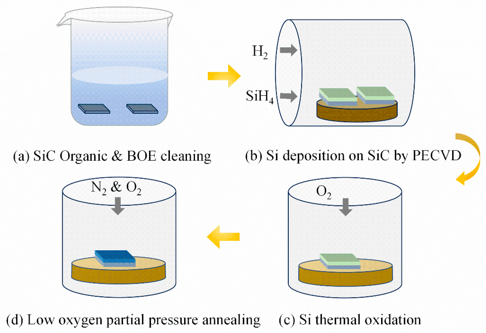
2. Materials and Methods

The procedures of the oxide layer formation and annealing process are shown in Figure 1. The N-type (8.0 × 1015 cm−3) 4H-SiC (0001) epitaxial layer was used in this work. After successive organic and buffered oxide etch (BOE, HF: NH4F = 1:7) cleaning, Si was deposited on the 4H-SiC wafer by introducing silane (SiH4) and H2 under 90 Pa at 200 °C for 8 min. The samples were oxidized in O2, resulting in an oxide layer with a thickness of 35 nm, which was calculated by C-V curves. Then, the oxidized samples were annealed in the mixture gas of N2 and O2 at 900, 1000, 1100, 1200, and 1250 °C for 10 min, respectively, in which the oxygen partial pressure was 0.01 Pa. To investigate the annealing mechanism at low oxygen partial pressure, the control samples were annealed in a vacuum (3 × 10⁻³ Pa). Finally, the Al electrode was deposited to form the SiC MOS capacitors.
The capacitance–voltage (C-V) curves were characterized by Keysight E4990 LCR. The high–low method was used to calculate the interface state density (Dit) [20], which represents the number of defects at the interface. The change in the fixed charge density in the oxide layer during annealing was observed with the ideal flat band voltage (VFB) [21,22] as the reference. XPS measurement was performed to analyze the composition of oxide layer elements. The ESCALAB 250Xi system carrying a monochromatic Kα line from an Al anode of 197 W was used to collect spectra. In addition, ToF-SIMS was performed to characterize the element distribution of the oxide layer in a more accurate way. The ToF-SIMS 5–100 instrument equipped with a Cs+ 1 keV ion beam for depth profiling was used to characterize the element distribution of oxide layers.
In order to confirm that N2 only acts as a protective gas without participating in the reaction during the annealing process, XPS characterization was used to analyze the elemental composition of the SiO2/SiC gate stack. The in situ etching of the Ar+ ion beam was used to gradually remove the oxide layer. Figure 2 shows the N 1s spectra and atomic percent of Si, O, C, and N elements of the samples without and with annealing in N2 at 1250 °C. The XPS result reveals that no N 1s peak can be detected either in the bulk of SiO2 or at the SiO2/SiC interface for samples without and with annealing. It confirms that the annealing process does not introduce N atoms into the SiO2/SiC stack and N2 only acts as a protective gas.

3. Results and Discussion

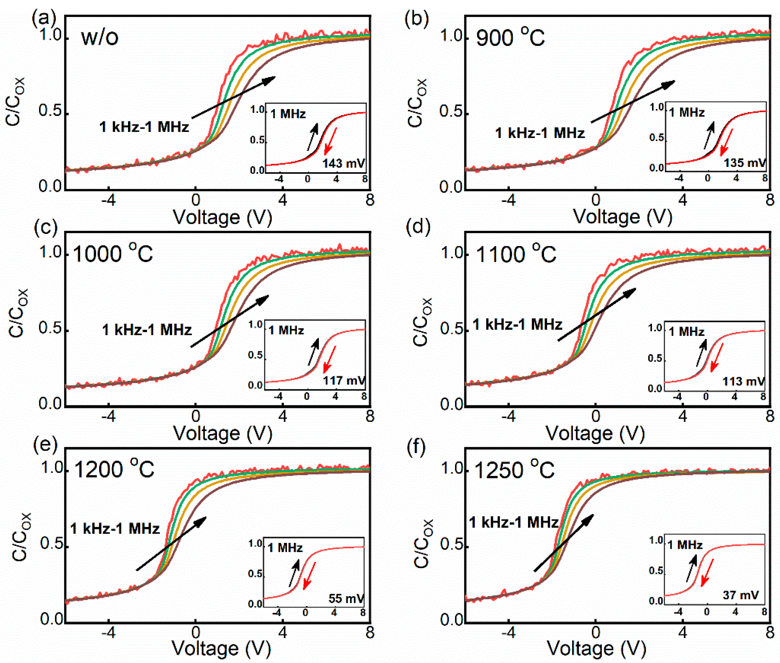
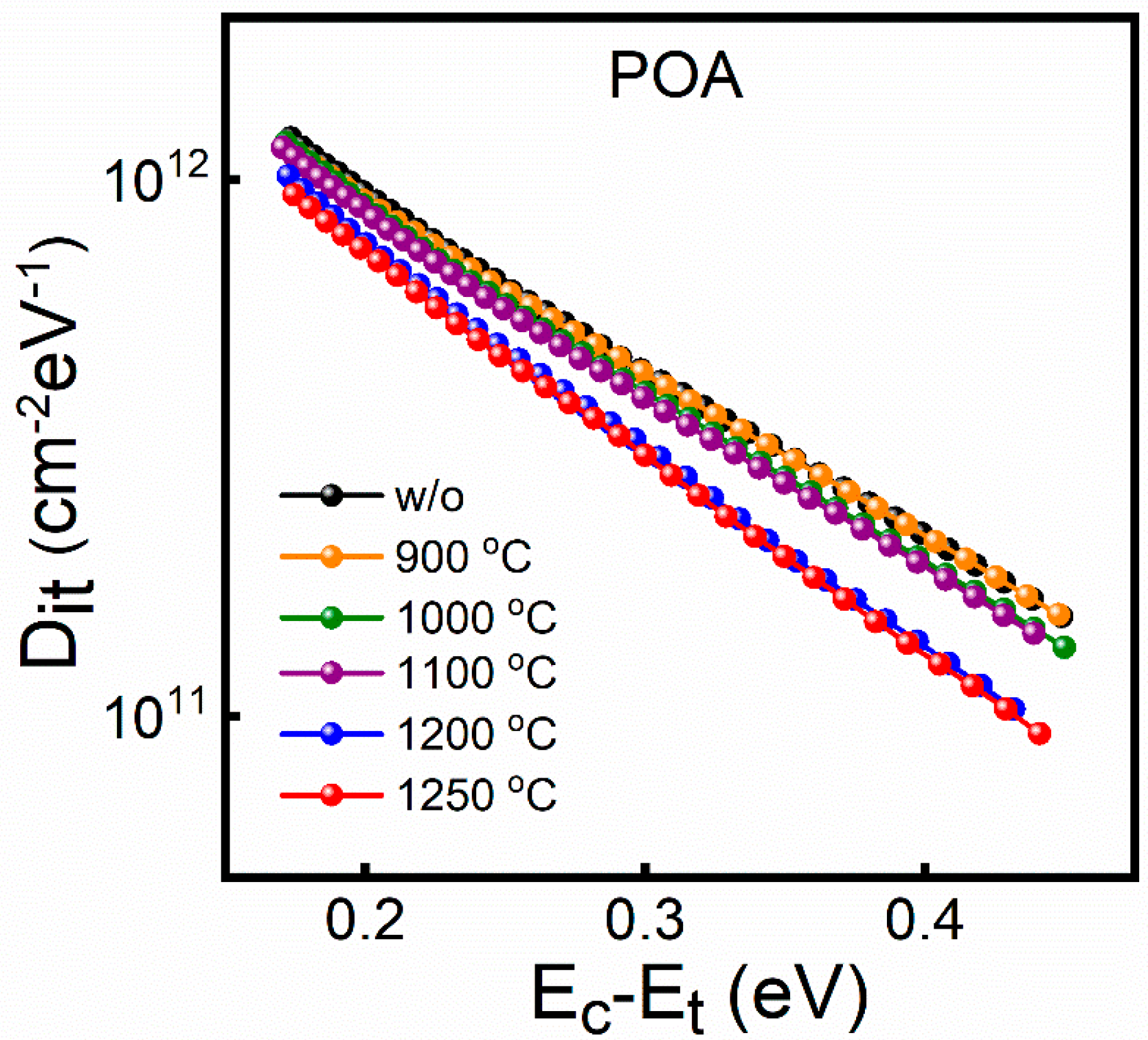
3.1. Effect of Low Oxygen Partial Pressure Annealing at Different Temperatures

Figure 3a–f show the multi-frequency C-V curves of the samples without and with annealing at 900–1250 °C. The process of charging and discharging of the traps at the interface occurs during the C-V measurements, resulting in the stretching out of the C-V curves in terms of voltage [23,24], which has an effect on the dispersion of C-V curves. In addition, the charge trapping of the defects near the interface under bias stress leads to the instability of the flat band voltage [25], and the defects can be evaluated by the hysteresis at high frequency [25,26]. Therefore, the frequency dispersion and hysteresis of the C-V curves can qualitatively represent the defects at and near the interface. The large frequency dispersion and hysteresis imply the existence of a high-defect value. Comparing with the unannealed sample, the annealed samples have smaller frequency dispersion and hysteresis, which indicates that the annealing process is effective in improve the quality of the SiC MOS. Additionally, the frequency dispersion and the hysteresis decrease with increasing POA temperature, indicating that the annealing effect is temperature-dependent. In the range of 900–1250 °C, the improvement effect is more pronounced with the increase in temperature.
In order to further quantitatively analyze the interface defects, the Dit value evaluated by the high–low C-V method is shown in Figure 4. Compared to the unannealed samples, the Dit values of the annealed samples decrease slightly with increased temperature, within the temperature range of 900–1100 °C, and decrease significantly at ≥1200 °C. The interface quality can be evaluated by the Dit value. The decrease in the Dit value indicates that the defects at the interface are repaired during the annealing process, which leads to the improvement in the interface quality. Therefore, the change trend of Dit proves that the annealing process with a low oxygen partial pressure improves the interface quality, and the improvement effect is more obvious at ≥1200 °C.
In order to assess the oxide layer quality, the defects near the interface and the shift of the VFB of the samples were investigated. The defects near the interface can be quantitatively evaluated by border trap density (Nbt), which can be estimated according to the integration area of the 1 MHz bidirectional C-V curves [27], as shown in the inset of Figure 3. In Figure 5a, the Nbt decreases with the increase in annealing temperature. There is a significant reduction in Nbt at 1200 °C, which is consistent with the trend of Dit in Figure 4. Therefore, for the repair of defects at and near the interface, the effect of low oxygen partial pressure annealing is significant when the temperature is up to 1200 °C. The change in the oxide layer charge can be analyzed by comparing the shift between the VFB of the annealed samples and the ideal value. Figure 5b shows the 1 MHz C-V curves of the annealed samples at different temperatures and a shift in the VFB from the ideal value can be observed. The 1 MHz C-V curve of the annealed samples shifts to the left with increasing temperature, suggesting that negative charge is removed during the annealing process. In other words, the low oxygen partial pressure annealing process is beneficial for the repair of charge defects in the oxide layer. It is worth noting that the charges in the oxide layer are generated in the process of thermal oxidation [28], which is related to the traps at and near the interface [29,30]. In addition, the repair of the oxide layer charge during the annealing process is not significant at <1100 °C, as indicated by the lateral shift of the C-V curve.
The above analysis shows that both the Dit and Nbt values of the annealed samples are decreased compared to the unannealed samples and the oxide layer charge also can be repaired, indicating that low oxygen partial pressure annealing can reduce traps and improve the quality of the interface and oxide layer. From the point of view of the dependence of the improvement effect and temperature, it is necessary to reach a certain temperature (≥1200 °C) for the improvement effect to be significant.

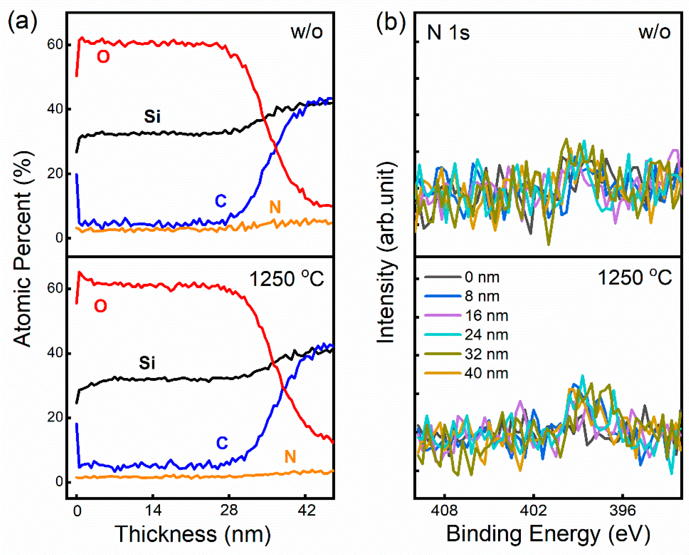
3.2. Annealing Mechanism of Low Oxygen Partial Pressure at Different Temperatures

Based on the role of oxygen and the improvement in the interface quality, we speculate that there are two possible repair mechanisms: volatilization, and the filling of oxygen vacancies (V[O]). It has been reported that the volatilization of V[O] at the interface can reduce the Dit value when the samples are annealed in an anoxic atmosphere [31]. To verify whether the V[O] volatilization applies to the low oxygen partial pressure annealing mechanism, the sample annealed in the vacuum (3 × 10⁻³ Pa) at 1200 °C was used as the control group. The vacuum is conducive to the volatilization of oxygen vacancies because it contains a lower oxygen partial pressure. Therefore, if the V[O] volatilization is the dominant mechanism, the Dit value should be reduced after vacuum annealing at the same temperature. However, as shown in Figure 6, samples without and with vacuum annealing have almost the same Dit, indicating that the V[O] volatilization is not the dominant mechanism during the annealing process.
In order to analyze the possibility of the V[O] filling, ToF-SIMS characterization was performed to obtain the depth distribution of silicon oxides with different chemical structures. Figure 7a shows the intensity ratio of SiO2 (Si4+) in the oxide layer of the sample without and with annealing at 1200 °C. The depth is the distance between the detection position and the SiO2/SiC interface, and the interface position is defined as a depth of 0 nm. Compared with the unannealed samples, the SiO2 ratio increases for the annealed samples, indicating that the quality of the oxide layer is improved during the annealing process. Figure 7b shows the depth distribution of oxides corresponding to the intermediate states Si3+, Si2+, and Si1+ of Si, respectively, which represent the V[O] distribution. The intermediate oxides of both samples have a ratio peak near the interface, indicating that the number of V[O] is the highest near the interface. The intensity ratio peak of the intermediate oxide of the annealed samples is lower than that of the unannealed samples, indicating that the V[O] can be reduced during the annealing process. Based on the above analysis, we suggest that the V[O] filling near the interface is the dominant mechanism due to low oxygen partial pressure. The V[O] near the interface is filled more by O2 in the annealing atmosphere with the increase in temperature and the V[O] decreases significantly at ≥1200 °C, which is consistent with the trend of the values of Dit and Nbt as a function of annealing temperature.

4. Conclusions

In summary, low oxygen partial pressure annealing at different temperatures has been demonstrated to be an effective way to improve the interface quality of the SiO2/SiC gate stack. The decrease in the Dit and Nbt values show that the defects are repaired during the annealing process. Both of the Dit and Nbt values decrease significantly, implying that the improvement effect is more obvious at ≥1200 °C. The XPS results show that no N 1s peak is detected in the oxide layer of the annealed sample, which confirms that N2 only acts as a protective gas and does not participate in the passivation reaction. The mechanism of V[O] volatilization is excluded due to almost the same Dit value for the samples without and with annealing in the vacuum. The ToF-SIMS analysis results show an increased intensity ratio of SiO2 in the oxide layer and a decreased intensity ratio of intermediate state oxides at the interface for the sample annealed at 1200 °C. Therefore, we infer that oxygen filling V[O] is the dominant mechanism of the interface improvement during the low oxygen partial pressure annealing process and more V[O] are filled as the temperature increases in the range of 900–1250 °C.

Author Contributions

Conceptualization, Q.Z. and N.Y.; methodology, Q.Z.; software, Q.Z.; validation, J.W., Y.X. and K.Z.; formal analysis, N.Y.; investigation, Q.Z.; resources, S.W.; data curation, Q.Z. and K.Z.; writing—original draft preparation, Q.Z.; writing—review and editing, Q.Z.; visualization, N.Y. and J.W.; supervision, S.W.; project administration, S.W.; funding acquisition, S.W. and N.Y. All authors have read and agreed to the published version of the manuscript.

Funding

This research was funded by the Beijing Municipal Natural Science Foundation, No. 4234091, the National Natural Science Foundation of China, No. 61974159, 62174176, and 62304245, the Scientific Instrument Developing Project of the Chinese Academy of Sciences (CAS), No. YJKYYQ20200039, and the Outstanding Member Project of the Youth Innovation Promotion Association of CAS, No. Y2021046.

Data Availability Statement

Data are contained within the article.

Conflicts of Interest

The authors declare no conflicts of interest.

References

  1. Kimoto, T. Bulk and epitaxial growth of silicon carbide. Prog. Cryst. Growth Charact. Mater. 2016, 62, 329–351. [Google Scholar] [CrossRef]
  2. Stefanakis, D.; Chi, X.; Maeda, T.; Kaneko, M.; Kimoto, T. Experimental determination of impact ionization coefficients along (1120) in 4H-SiC. IEEE Trans. Electron Devices 2020, 67, 3740–3744. [Google Scholar] [CrossRef]
  3. Matsunami, H. Fundamental research on semiconductor SiC and its applications to power electronics. Proc. Jpn. Acad. Ser. B 2020, 96, 235–254. [Google Scholar] [CrossRef]
  4. Xie, Y.; Chen, C.; Yan, Y.Y.; Huang, Z.Z.; Kang, Y. Investigation on Ultralow Turn-off Losses Phenomenon for SiC MOSFETs With Improved Switching Model. IEEE Trans. Power Electron. 2021, 36, 9382–9397. [Google Scholar] [CrossRef]
  5. Kimoto, T. High-voltage SiC power devices for improved energy efficiency. Proc. Jpn. Acad. Ser. B 2022, 98, 161–189. [Google Scholar] [CrossRef]
  6. Arnold, E.; Alok, D. Effect of interface states on electron transport in 4H-SiC inversion layers. IEEE Trans. Electron Devices 2001, 48, 1870. [Google Scholar] [CrossRef]
  7. Yoshioka, H.; Senzaki, J.; Shimozato, A.; Tanaka, Y.; Okumura, H. N-channel field- effect mobility inversely proportional to the interface state density at the conduction band edges of SiO2/4H-SiC interfaces. AIP Adv. 2015, 5, 017109. [Google Scholar] [CrossRef]
  8. Hatakeyama, T.; Kiuchi, Y.; Sometani, M.; Harada, S.; Okamoto, D.; Yano, H.; Yonezawa, Y.; Okumura, H. Characterization of traps at nitrided SiO2/SiC interfaces near the conduction band edge by using Hall effect measurements. Appl. Phys. Express 2017, 10, 046601. [Google Scholar] [CrossRef]
  9. Kobayashi, T.; Okuda, T.; Tachiki, K.; Ito, K.; Matsushita, Y.I.; Kimoto, T. Design and formation of SiC (0001)/SiO2 interfaces via Si deposition followed by low temperature oxidation and high-temperature nitridation. Appl. Phys. Express 2020, 13, 091003. [Google Scholar] [CrossRef]
  10. Liu, X.Y.; Hao, J.L.; You, N.N.; Bai, Y.; Wang, S.K. High-pressure microwave plasma oxidation of 4H-SiC with low interface trap density. AIP Adv. 2019, 9, 125150. [Google Scholar] [CrossRef]
  11. Morishita, R.; Yano, H.; Okamoto, D.; Hatayama, T.; Fuyuki, T. Effect of POCl3 Annealing on Reliability of Thermal Oxides Grown on 4H-SiC. Mater. Sci. Forum 2012, 717, 739–742. [Google Scholar] [CrossRef]
  12. Jamet, P.; Dimitrijev, S.; Tanner, P. Effects of nitridation in gate oxides grown on 4H-SiC. J. Appl. Phys. 2001, 90, 5058–5063. [Google Scholar] [CrossRef]
  13. Chung, G.Y.; Tin, C.C.; Williams, J.R.; Mcdonald, K.; Palmour, J.W. Improved inversion channel mobility for 4H-SiC MOSFETs following high temperature anneals in nitric oxide. IEEE Electron Device Lett. 2001, 22, 176–178. [Google Scholar] [CrossRef]
  14. Kimoto, T.; Kanzaki, Y.; Noborio, M.; Kawano, H.; Matsunami, H. Interface Properties of Metal–Oxide–Semiconductor Structures on 4H-SiC {0001} and (1120) Formed by N2O Oxidation. Jpn. J. Appl. Phys. 2005, 44, 1213–1218. [Google Scholar] [CrossRef]
  15. Shirasawa, T.; Hayashi, K.; Mizuno, S.; Tanaka, S.; Nakatsuji, K.; Komori, F.; Tochihara, H. Epitaxial Silicon Oxynitride Layer on a 6H−SiC (0001) Surface. Phys. Rev. Lett. 2007, 98, 136105. [Google Scholar] [CrossRef] [PubMed]
  16. Xu, Y.; Zhu, X.; Lee, H.D.; Xu, C.; Shubeita, S.M.; Ahyi, A.C.; Sharma, Y.; Williams, J.R.; Lu, W.; Ceesay, S.; et al. Atomic state and characterization of nitrogen at the SiC/SiO2 interface. J. Appl. Phys. 2014, 115, 033502. [Google Scholar] [CrossRef]
  17. Kao, W.C.; Goryll, M.; Marinella, M.; Kaplar, R.J.; Jiao, C.; Dhar, S.; Cooper, J.A.; Schroder, D.K. Characterization of fast interface states in nitrogen- and phosphorus-treated 4H-SiC MOS capacitors. Semicond. Sci. Technol. 2015, 30, 075011. [Google Scholar] [CrossRef]
  18. Zhang, Q.; You, N.N.; Liu, P.; Wang, J.Y.; Xu, Y.; Wang, S.K. Study of defects distribution in SiO2/SiC with plasma oxidation and post oxidation annealing. Appl. Surf. Sci. 2023, 610, 155500. [Google Scholar] [CrossRef]
  19. Kobayashi, T.; Tachiki, K.; Ito, K.; Kimoto, T. Reduction of interface state density in SiC (0001) MOS structures by low-oxygen-partial-pressure annealing. Appl. Phys. Express 2019, 12, 031001. [Google Scholar] [CrossRef]
  20. Ziegler, K.; Klausmann, E. Static technique for precise measurements of surface potential and interface state density in MOS structures. Appl. Phys. Lett. 1975, 26, 400–402. [Google Scholar] [CrossRef]
  21. Southwick, R.G., III; Knowlton, W.B. Stacked dual oxide MOS energy band diagram visual representation program. IEEE Trans. Device Mater. Reliab. 2006, 6, 136–145. [Google Scholar] [CrossRef]
  22. Southwick, R.G., III; Sup, A.; Jain, A.; Knowlton, W.B. An interactive simulation tool for complex multilayer dielectric devices. IEEE Trans. Device Mater. Reliab. 2011, 11, 236–243. [Google Scholar] [CrossRef]
  23. Nicollian, E.H.; Brews, J.R. MOS (Metal Oxide Semiconductor) Physics and Technology; Wiley: Hoboken, NJ, USA, 1982; pp. 176–230. [Google Scholar]
  24. Berglund, C.N. Surface states at steam-grown silicon-silicon dioxide interfaces. IEEE Trans. Electron Devices 1966, ED-13, 701–705. [Google Scholar] [CrossRef]
  25. Lelis, A.J.; Habersat, D.; Green, R.; Ogunniyi, A.; Gurfinkel, M.; Suehle, J.; Goldsman, N. Time Dependence of Bias-Stress-Induced SiC MOSFET Threshold-Voltage Instability Measurements. IEEE Trans. Electron Devices 2008, 55, 1835–1840. [Google Scholar] [CrossRef]
  26. Evangelou, E.K.; Rahman, M.S.; Dimoulas, A. Correlation of Charge Buildup and Stress-Induced Leakage Current in Cerium Oxide Films Grown on Ge (100) Substrates. IEEE Trans. Electron Devices 2009, 56, 399–407. [Google Scholar] [CrossRef]
  27. Fleetwood, D.M.; Saks, N.S. Oxide, interface, and border traps in thermal, N2O, and N2O-nitrided oxides. J. Appl. Phys. 1996, 79, 1583–1594. [Google Scholar] [CrossRef]
  28. Pitthan, E.; Lopes, L.D.; Palmieri, R.; Corrêa, S.A.; Soares, G.V.; Boudinov, H.I.; Stedile, F.C. Influence of thermal growth parameters on the SiO2/4H-SiC interfacial region. APL Mater. 2013, 1, 022101. [Google Scholar] [CrossRef]
  29. Agarwal, A.K.; Haney, S. Some critical materials and processing issues in SiC power devices. J. Electron. Mater. 2008, 37, 646–654. [Google Scholar] [CrossRef]
  30. Lelis, A.J.; Green, R.; Habersat, D.B.; El, M. Basic mechanisms of threshold-voltage instability and implications for reliability testing of SiC MOSFETs. IEEE Trans. Electron Devices 2015, 62, 316–323. [Google Scholar] [CrossRef]
  31. Wang, S.K.; Kita, K.; Lee, C.H.; Tabata, T.; Nishimura, T.; Nagashio, K.; Toriumi, A. Desorption kinetics of GeO from GeO2/Ge structure. J. Appl. Phys. 2010, 108, 054104. [Google Scholar] [CrossRef]
Figure 1. Schematic diagram of SiO2/SiC structure formation and annealing process.
Nanomaterials 14 00192 g001
Figure 2. (a) The atomic percent of Si, O, C, and N elements and (b) the N 1s peak of the samples without and with annealing at 1250 °C.
Nanomaterials 14 00192 g002
Figure 3. The multi-frequency C-V curves from 1 kHz to 1 MHz for the samples (a) without annealing and with annealing at (b) 900 °C, (c) 1000 °C, (d) 1100 °C, (e) 1200 °C, and (f) 1250 °C. Bidirectional C-V curves measured at 1 MHz are shown in the inset.
Nanomaterials 14 00192 g003
Figure 4. The Dit calculated by the high–low method for the sample annealed from 900 to 1250 °C, respectively.
Nanomaterials 14 00192 g004
Figure 5. (a) Border trap density (Nbt) and (b) 1 MHz C-V curves of annealed samples at different temperatures.
Nanomaterials 14 00192 g005
Figure 6. The Dit of the samples without and with annealing in vacuum at 1200 °C.
Nanomaterials 14 00192 g006
Figure 7. The depth distribution of oxides corresponding to the valence states (a) Si4+, (b) Si3+, Si2+, and Si1+ of Si, respectively.
Nanomaterials 14 00192 g007
Disclaimer/Publisher’s Note: The statements, opinions and data contained in all publications are solely those of the individual author(s) and contributor(s) and not of MDPI and/or the editor(s). MDPI and/or the editor(s) disclaim responsibility for any injury to people or property resulting from any ideas, methods, instructions or products referred to in the content.

