Interface Properties of MoS2 van der Waals Heterojunctions with GaN

 ,
,  ,
,  ,
,  ,
,  ,
,  ,
,  ,
,  , and
, and 
Abstract
1. Introduction
2. Materials and Methods
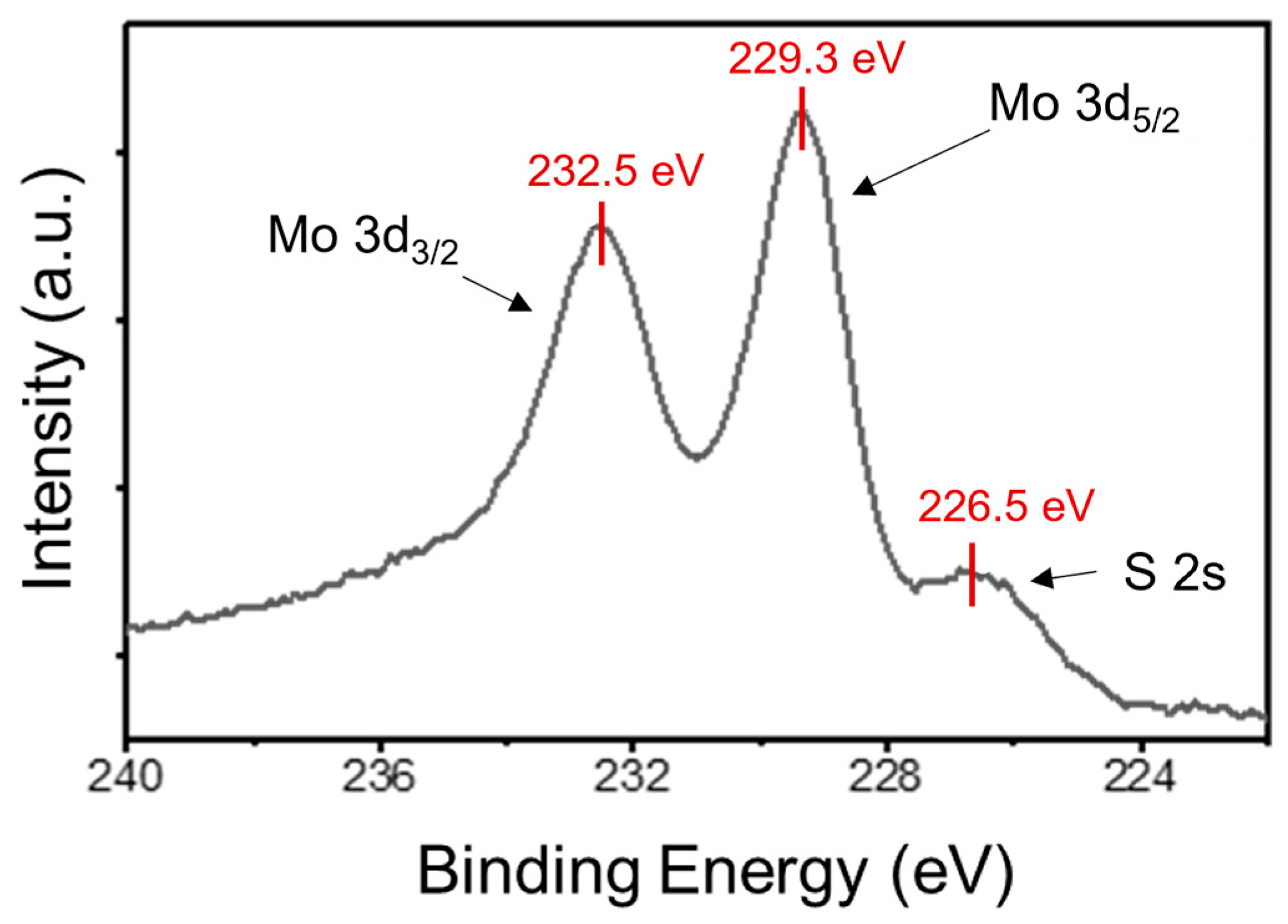
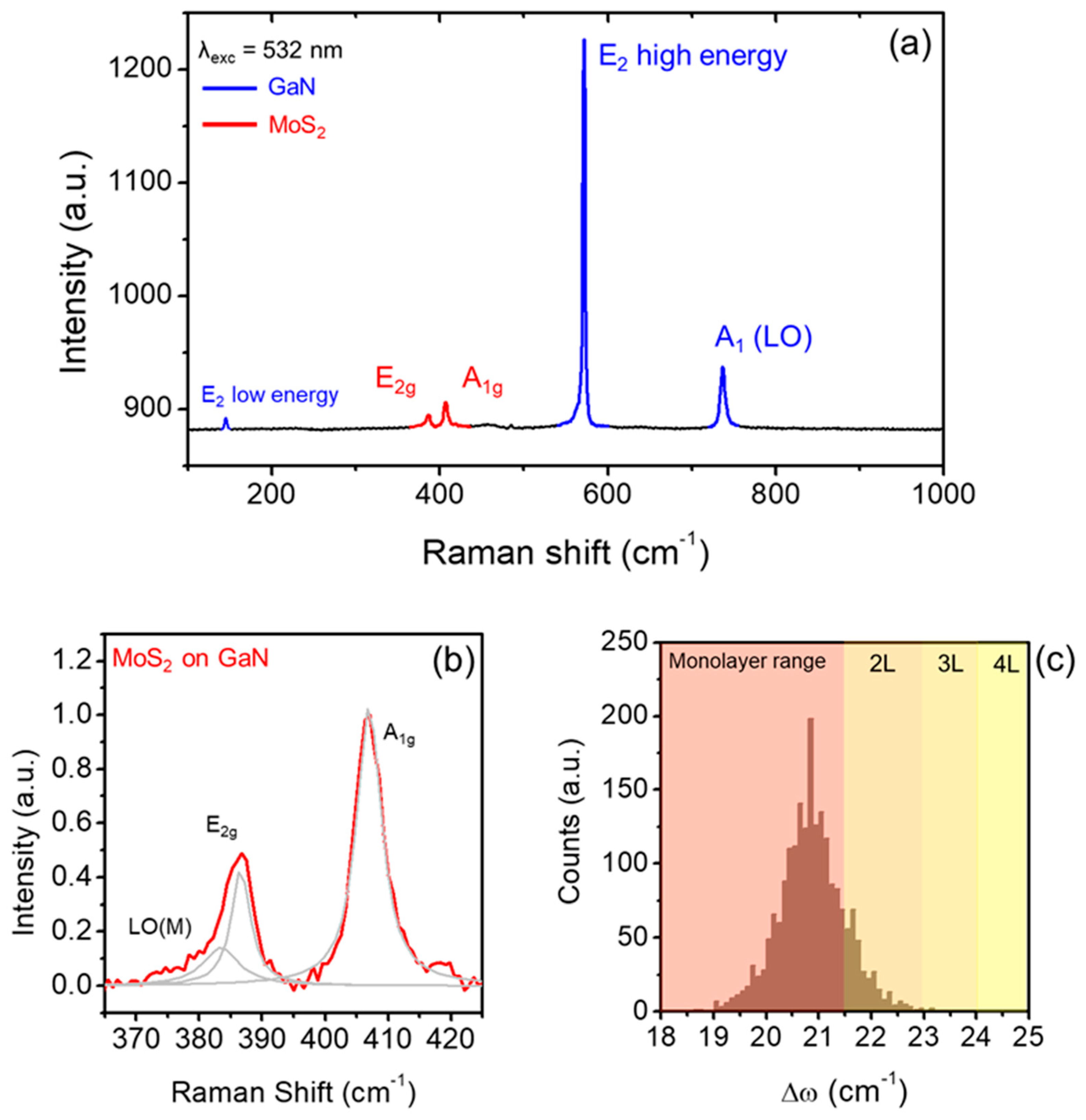
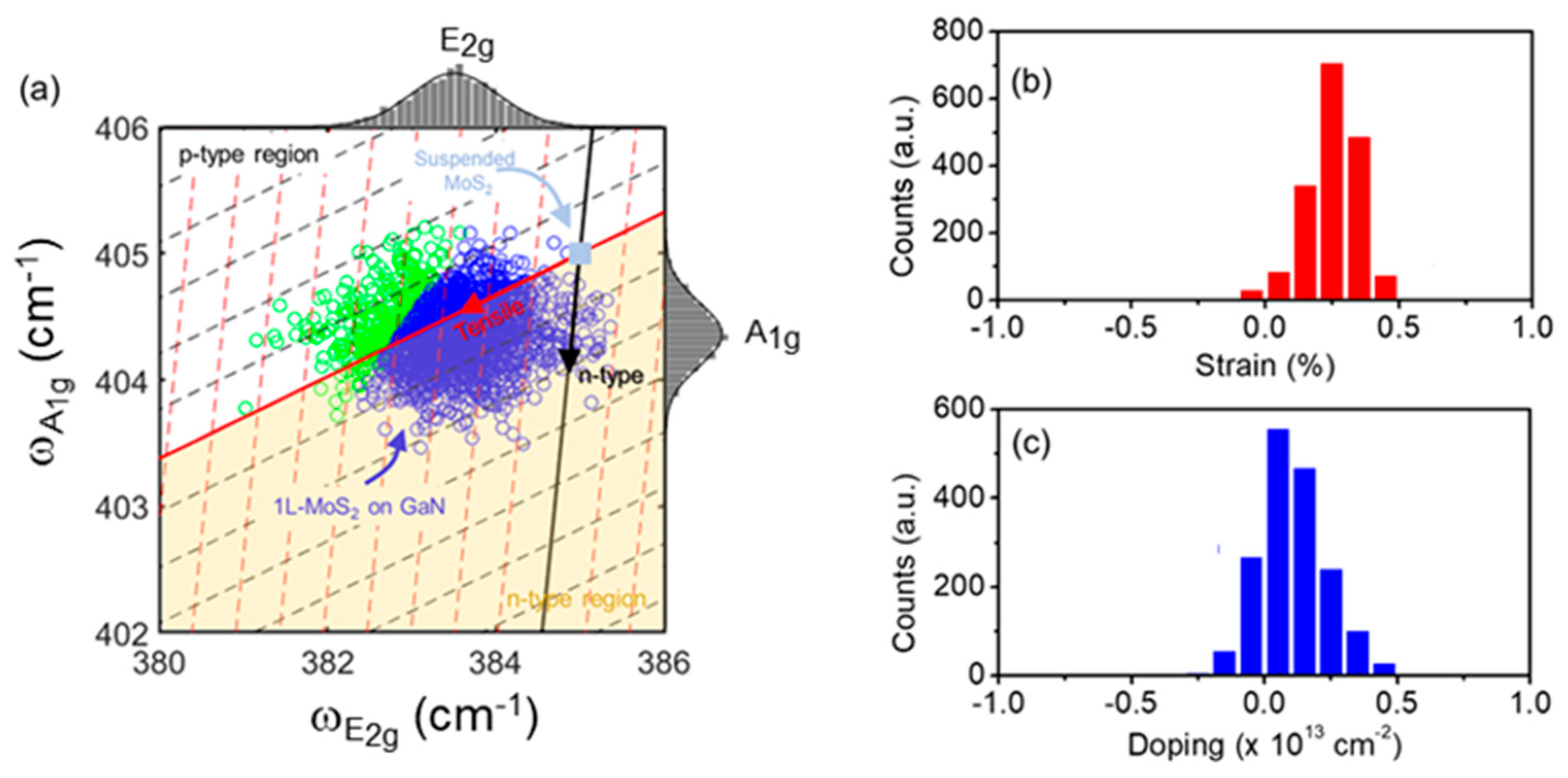
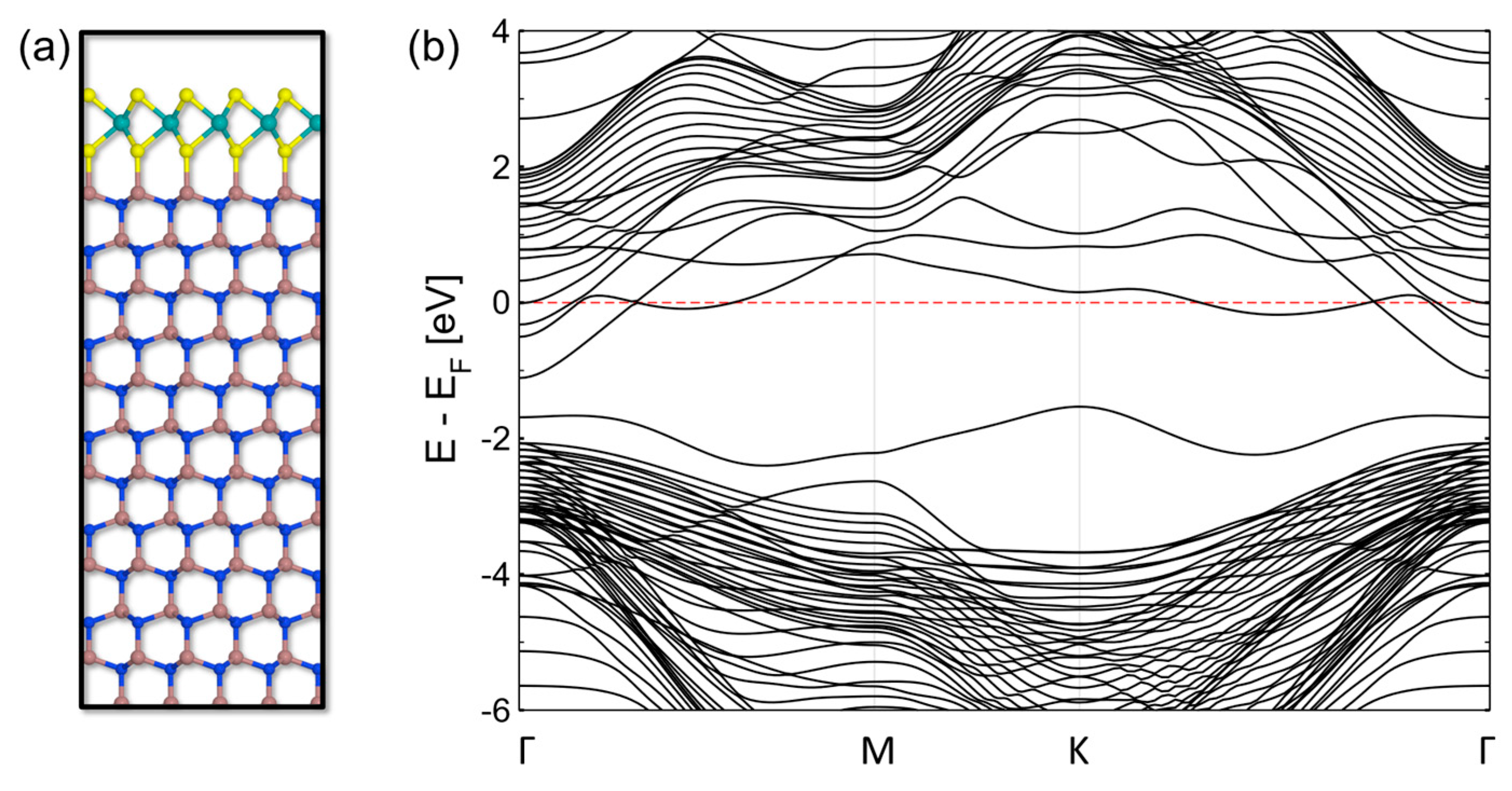
3. Results
4. Conclusions
Supplementary Materials
Author Contributions
Funding
Data Availability Statement
Acknowledgments
Conflicts of Interest
References
- Radisavljevic, B.; Radenovic, A.; Brivio, J.; Giacometti, V.; Kis, A. Single-layer MoS2 transistors. Nat. Nanotechnol. 2011, 6, 147–150. [Google Scholar] [CrossRef]
- Geim, A.K.; Grigorieva, I.V. Van der Waals heterostructures. Nature 2013, 499, 419–425. [Google Scholar] [CrossRef]
- Kolobov, A.V.; Tominaga, J. Two-Dimensional Transition-Metal Dichalcogenides; Springer: Berlin/Heidelberg, Germany, 2016; Volume 239. [Google Scholar]
- Jariwala, D.; Sangwan, V.K.; Lauhon, L.J.; Marks, T.J.; Hersam, M.C. Emerging device applications for semiconducting two-dimensional transition metal dichalcogenides. ACS Nano 2014, 8, 1102–1120. [Google Scholar] [CrossRef]
- Nawz, T.; Safdar, A.; Hussain, M.; Lee, S.D.; Siyar, M. Graphene to advanced MoS2: A review of structure, synthesis, and optoelectronic device application. Crystals 2020, 10, 902. [Google Scholar] [CrossRef]
- Splendiani, A.; Sun, L.; Zhang, Y.; Li, T.; Kim, J.; Chim, C.Y.; Galli, G.; Wang, F. Emerging photoluminescence in monolayer MoS2. Nano Lett. 2010, 10, 1271–1275. [Google Scholar] [CrossRef]
- Mak, K.F.; Lee, C.; Hone, J.; Shan, J.; Heinz, T.F. Atomically thin MoS2: A new direct-gap semiconductor. Phys. Rev. Lett. 2010, 105, 136805. [Google Scholar] [CrossRef]
- Zeng, S.; Tang, Z.; Liu, C.; Zhou, P. Electronics based on two-dimensional materials: Status and outlook. Nano Res. 2021, 14, 1752–1767. [Google Scholar] [CrossRef]
- Radisavljevic, B.; Whitwick, M.B.; Kis, A. Integrated circuits and logic operations based on single-layer MoS2. ACS Nano 2011, 5, 9934–9938. [Google Scholar] [CrossRef]
- Lopez-Sanchez, O.; Lembke, D.; Kayci, M.; Radenovic, A.; Kis, A. Ultrasensitive photodetectors based on monolayer MoS2. Nat. Nanotechnol. 2013, 8, 497–501. [Google Scholar] [CrossRef]
- Wang, Q.H.; Kalantar-Zadeh, K.; Kis, A.; Coleman, J.N.; Strano, M.S. Electronics and optoelectronics of two-dimensional transition metal dichalcogenides. Nat. Nanotechnol. 2012, 7, 699–712. [Google Scholar] [CrossRef]
- Singh, E.; Singh, P.; Kim, K.S.; Yeom, G.Y.; Nalwa, H.S. Flexible molybdenum disulfide (MoS2) atomic layers for wearable electronics and optoelectronics. ACS Appl. Mater. Interf. 2019, 11, 11061–11105. [Google Scholar] [CrossRef]
- Late, D.J.; Huang, Y.K.; Liu, B.; Acharya, J.; Shirodkar, S.N.; Luo, J.; Yan, A.; Charles, D.; Waghmare, U.V.; Dravid, V.P.; et al. Sensing behavior of atomically thin-layered MoS2 transistors. ACS Nano 2013, 7, 4879–4891. [Google Scholar] [CrossRef]
- Perkins, F.K.; Friedman, A.L.; Cobas, E.; Campbell, P.M.; Jernigan, G.G.; Jonker, B.T. Chemical vapor sensing with monolayer MoS2. Nano Lett. 2013, 13, 668–673. [Google Scholar] [CrossRef]
- Chang, K.; Mei, Z.; Wang, T.; Kang, Q.; Ouyang, S.; Ye, J. MoS2/graphene cocatalyst for efficient photocatalytic H2 evolution under visible light irradiation. ACS Nano 2014, 8, 7078–7087. [Google Scholar] [CrossRef]
- Parzinger, E.; Miller, B.; Blaschke, B.; Garrido, J.A.; Ager, J.W.; Holleitner, A.; Wurstbauer, U. Photocatalytic stability of single-and few-layer MoS2. ACS Nano 2015, 9, 11302–11309. [Google Scholar] [CrossRef]
- Wi, S.; Kim, H.; Chen, M.; Nam, H.; Guo, L.J.; Meyhofer, E.; Liang, X. Enhancement of photovoltaic response in multilayer MoS2 induced by plasma doping. ACS Nano 2014, 8, 5270–5281. [Google Scholar] [CrossRef]
- Lopez-Sanchez, O.; Llado, A.E.; Koman, V.; Fontcuberta i Morral, A.; Radenovic, A.; Kis, A. Light generation and harvesting in a van der Waals heterostructure. ACS Nano 2014, 8, 3042–3048. [Google Scholar] [CrossRef]
- Xia, F.; Wang, H.; Xiao, D.; Dubey, M.; Ramasubramaniam, A. Two-dimensional material nanophotonics. Nat. Phot. 2014, 8, 899–907. [Google Scholar] [CrossRef]
- Low, T.; Chaves, A.; Caldwell, J.D.; Kumar, A.; Fang, N.X.; Avouris, P.; Heinz, T.Y.; Guinea, F.; Martin-Moreno, L.; Koppens, F. Polaritons in layered two-dimensional materials. Nat. Mater. 2017, 16, 182–194. [Google Scholar] [CrossRef]
- Xu, X.; Yao, W.; Xiao, D.; Heinz, T.F. Spin and pseudospins in layered transition metal dichalcogenides. Nat. Phys. 2014, 10, 343–350. [Google Scholar] [CrossRef]
- Mak, K.F.; He, K.; Shan, J.; Heinz, T.F. Control of valley polarization in monolayer MoS2 by optical helicity. Nat. Nanotechnol. 2012, 7, 494–498. [Google Scholar] [CrossRef]
- Mak, K.F.; Xiao, D.; Shan, J. Light–valley interactions in 2D semiconductors. Nat. Photonics 2018, 12, 451–460. [Google Scholar] [CrossRef]
- Kim, J.; Jin, C.; Chen, B.; Cai, H.; Zhao, T.; Lee, P.; Khan, S.; Watanabe, K.; Taniguchi, T.; Tongay, S.; et al. Observation of ultralong valley lifetime in WSe2/MoS2 heterostructures. Sci. Adv. 2017, 3, e1700518. [Google Scholar] [CrossRef]
- Yu, L.; Lee, Y.H.; Ling, X.; Santos, E.J.; Shin, Y.C.; Lin, Y.; Dubey, M.; Kaxiras, E.; Kong, J.; Wang, H.; et al. Graphene/MoS2 hybrid technology for large-scale two-dimensional electronics. Nano Lett. 2014, 14, 3055–3063. [Google Scholar] [CrossRef]
- Cho, B.; Yoon, J.; Lim, S.K.; Kim, A.R.; Kim, D.H.; Park, S.G.; Kwon, J.D.; Lee, Y.J.; Lee, K.H.; Lee, B.H.; et al. Chemical sensing of 2D graphene/MoS2 heterostructure device. ACS Appl. Mater. Interf. 2015, 7, 16775–16780. [Google Scholar] [CrossRef]
- Kistanov, A.A.; Shcherbinin, S.A.; Ustiuzhanina, S.V.; Huttula, M.; Cao, W.; Nikitenko, V.R.; Prezhdo, O.V. First-principles prediction of two-dimensional B3C2P3 and B2C4P2: Structural stability, fundamental properties, and renewable energy applications. J. Phys. Chem. Lett. 2021, 12, 3436–3442. [Google Scholar] [CrossRef]
- Liu, Y.; Weiss, N.O.; Duan, X.; Cheng, H.C.; Huang, Y.; Duan, X. Van der Waals heterostructures and devices. Nat. Rev. Mater. 2016, 1, 16042. [Google Scholar] [CrossRef]
- Jariwala, D.; Marks, T.J.; Hersam, M.C. Mixed-dimensional van der Waals heterostructures. Nat. Mater. 2017, 16, 170–181. [Google Scholar] [CrossRef]
- Wang, P.; Jia, C.; Huang, Y.; Duan, X. Van der Waals heterostructures by design: From 1D and 2D to 3D. Matter 2021, 4, 552–581. [Google Scholar] [CrossRef]
- Butanovs, E.; Kadiwala, K.; Gopejenko, A.; Bocharov, D.; Piskunov, S.; Polyakov, B. Different strategies for GaN-MoS2 and GaN-WS2 core–shell nanowire growth. Appl. Surf. Sci. 2022, 590, 153106. [Google Scholar] [CrossRef]
- Dezfuli, F.M.; Boochani, A.; Parhizgar, S.S.; Darabi, E. Electronic, optical and thermoelectric properties of MoS2-GaN interface, International. J. Mod. Phys. B 2022, 36, 2250096. [Google Scholar] [CrossRef]
- Kimoto, T.; Cooper, J.A. Fundamentals of Silicon Carbide Technology: Growth, Characterization, Devices and Applications; John Wiley & Sons: Hoboken, NJ, USA, 2014. [Google Scholar]
- Roccaforte, F.; Fiorenza, P.; Greco, G.; Lo Nigro, R.; Giannazzo, F.; Iucolano, F.; Saggio, M. Emerging trends in wide band gap semiconductors (SiC and GaN) technology for power devices. Microelectron. Eng. 2018, 187, 66–77. [Google Scholar] [CrossRef]
- Giannazzo, F.; Panasci, S.E.; Schilirò, E.; Roccaforte, F.; Koos, A.; Nemeth, M.; Pécz, B. Esaki diode behavior in highly uniform MoS2/silicon carbide heterojunctions. Adv. Mater. Interf. 2022, 9, 2200915. [Google Scholar] [CrossRef]
- Giannazzo, F.; Panasci, S.E.; Schilirò, E.; Greco, G.; Roccaforte, F.; Sfuncia, G.; Nicotra, G.; Cannas, M.; Agnello, S.; Frayssinet, E.; et al. Atomic resolution interface structure and vertical current injection in highly uniform MoS2 heterojunctions with bulk GaN. Appl. Surf. Sci. 2023, 631, 157513. [Google Scholar] [CrossRef]
- O’Regan, T.P.; Ruzmetov, D.; Neupane, M.R.; Burke, R.A.; Herzing, A.A.; Zhang, K.; Birdwell, A.G.; Taylor, D.E.; Byrd, E.F.C.; Walck, S.D.; et al. Structural and electrical analysis of epitaxial 2D/3D vertical heterojunctions of monolayer MoS2 on GaN. Appl. Phys. Lett. 2017, 111, 051602. [Google Scholar] [CrossRef]
- Liu, Y.; Fang, Y.; Yang, D.; Pi, X.; Wang, P. Recent progress of heterostructures based on two dimensional materials and wide bandgap semiconductors. J. Phys. Condens. Matter 2022, 34, 183001. [Google Scholar] [CrossRef]
- Singh, D.K.; Pant, R.K.; Nanda, K.K.; Krupanidhi, S.B. Differentiation of ultraviolet/visible photons from near infrared photons by MoS2/GaN/Si-based photodetector. Appl. Phys. Lett. 2021, 119, 121102. [Google Scholar] [CrossRef]
- Jain, S.K.; Low, M.X.; Taylor, P.D.; Tawfik, S.A.; Spencer, M.J.; Kuriakose, S.; Arash, A.; Xu, C.; Sriram, S.; Gupta, G.; et al. 2D/3D hybrid of MoS2/GaN for a high-performance broadband photodetector. ACS Appl. Elect. Mater. 2021, 3, 2407–2414. [Google Scholar] [CrossRef]
- Stockmeier, M.; Müller, R.; Sakwe, S.A.; Wellmann, P.J.; Magerl, A. On the lattice parameters of silicon carbide. J. Appl. Phys. 2009, 105, 033511. [Google Scholar] [CrossRef]
- Ruzmetov, D.; Zhang, K.; Stan, G.; Kalanyan, B.; Bhimanapati, G.R.; Eichfeld, S.M.; Burke, R.A.; Shah, P.B.; O’Regan, T.P.; Crowne, F.J.; et al. Vertical 2D/3D semiconductor heterostructures based on epitaxial molybdenum disulfide and gallium nitride. ACS Nano 2016, 10, 3580–3588. [Google Scholar] [CrossRef]
- Wan, Y.; Xiao, J.; Li, J.; Fang, X.; Zhang, K.; Fu, L.; Li, P.; Song, Z.; Zhang, H.; Wang, Y.; et al. Epitaxial Single-Layer MoS2 on GaN with Enhanced Valley Helicity. Adv. Mater. 2018, 30, 1703888. [Google Scholar] [CrossRef]
- Murray, R.; Evans, B. The thermal expansion of 2H-MoS2 and 2H-WSe2 between 10 and 320 K. J. Appl. Crystallogr. 1979, 12, 312. [Google Scholar] [CrossRef]
- Reeber, R.R.; Wang, K. Lattice parameters and thermal expansion of GaN. J. Mater. Res. 2000, 15, 40–44. [Google Scholar] [CrossRef]
- Moun, M.; Kumar, M.; Garg, M.; Pathak, R.; Singh, R. Understanding of MoS2/GaN heterojunction diode and its photodetection properties. Sci. Rep. 2018, 8, 11799. [Google Scholar] [CrossRef]
- Ruzmetov, D.; Neupane, M.R.; Herzing, A.; O’Regan, T.P.; Mazzoni, A.; Chin, M.L.; Burke, R.A.; Crowne, F.J.; Birdwell, A.G.; Taylor, D.E.; et al. Van der Waals interfaces in epitaxial vertical metal/2D/3D semiconductor heterojunctions of monolayer MoS2 and GaN. 2D Mater. 2018, 5, 045016. [Google Scholar] [CrossRef]
- Desai, P.; Ranade, A.K.; Shinde, M.; Todankar, B.; Mahyavanshi, R.D.; Tanemura, M.; Kalita, G. Growth of uniform MoS2 layers on free-standing GaN semiconductor for vertical heterojunction device application. J. Mater. Sci. Mater. Electron. 2020, 31, 2040–2048. [Google Scholar] [CrossRef]
- Krishnamoorthy, S.; Lee, E.W.; Lee, C.H.; Zhang, Y.; McCulloch, W.D.; Johnson, J.M.; Hwang, J.; Wu, Y.; Rajan, S. High current density 2D/3D MoS2/GaN Esaki tunnel diodes. Appl. Phys. Lett. 2016, 109, 183505. [Google Scholar] [CrossRef]
- Zhuo, R.; Wang, Y.; Wu, D.; Lou, Z.; Shi, Z.; Xu, T.; Xu, J.; Tian, Y.; Li, X. High-performance self-powered deep ultraviolet photodetector based on MoS2/GaN p–n heterojunction. J. Mater. Chem. C 2018, 6, 299–303. [Google Scholar] [CrossRef]
- Janardhanam, V.; Zummukhozol, M.; Jyothi, I.; Shim, K.H.; Choi, C.J. Self-powered MoS2/n-type GaN heterojunction photodetector with broad spectral response in ultraviolet–visible–near-infrared range. Sens. Actuators A Phys. 2023, 360, 114534. [Google Scholar] [CrossRef]
- Xue, F.; Yang, L.; Chen, M.; Chen, J.; Yang, X.; Wang, L.; Chen, L.; Pan, C.; Wang, Z.L. Enhanced photoresponsivity of the MoS2-GaN heterojunction diode via the piezo-phototronic effect. NPG Asia Mater. 2017, 9, e418. [Google Scholar] [CrossRef]
- Zahir, N.H.; Ripain, A.H.A.; Said, S.M.; Zakaria, R. Sulfurization engineering of single-zone CVD vertical and horizontal MoS2 on p-GaN heterostructures for self-powered UV photodetectors. Nanoscale Adv. 2023, 5, 879–892. [Google Scholar]
- Vashishtha, P.; Prajapat, P.; Sharma, A.; Singh, P.; Walia, S.; Gupta, G. Self-Driven UVC–NIR Broadband Photodetector with High-Temperature Reliability Based on a Coco Palm-Like MoS2/GaN Heterostructure. ACS Appl. Electr. Mater. 2023, 5, 1891–1902. [Google Scholar] [CrossRef]
- Yang, P.; Yang, H.; Wu, Z.; Liao, F.; Guo, X.; Deng, J.; Xu, Q.; Wang, H.; Sun, J.; Chen, F.; et al. Large-Area Monolayer MoS2 Nanosheets on GaN Substrates for Light-Emitting Diodes and Valley-Spin Electronic Devices. ACS Appl. Nano Mater. 2021, 4, 12127–12136. [Google Scholar] [CrossRef]
- Gao, R.; Liu, H.; Liu, H.; Yang, J.; Yang, F.; Wang, T. Two-dimensional MoS2/GaN van der Waals heterostructures: Tunable direct band alignments and excitonic optical properties for photovoltaic applications. J. Phys. D Appl. Phys. 2020, 53, 095107. [Google Scholar] [CrossRef]
- Poudel, Y.; Sławińska, J.; Gopal, P.; Seetharaman, S.; Hennighausen, Z.; Kar, S.; D’souza, F.; Nardelli, M.B.; Neogi, A. Absorption and emission modulation in a MoS2–GaN (0001) heterostructure by interface phonon–exciton coupling. Photonics Res. 2019, 7, 1511–1520. [Google Scholar] [CrossRef]
- Henck, H.; Aziza, Z.B.; Zill, O.; Pierucci, D.; Naylor, C.H.; Silly, M.G.; Gogneau, N.; Oehler, F.; Collin, S.; Brault, J.; et al. Interface dipole and band bending in the hybrid p−n heterojunction MoS2/GaN (0001). Phys. Rev. B 2017, 96, 115312. [Google Scholar] [CrossRef]
- Zhang, Z.; Qian, Q.; Li, B.; Chen, K.J. Interface Engineering of Monolayer MoS2/GaN Hybrid Heterostructure: Modified Band Alignment for Photocatalytic Water Splitting Application by Nitridation Treatment. ACS Appl. Mater. Interf. 2018, 10, 17419–17426. [Google Scholar] [CrossRef]
- Giannozzi, P.; Baroni, S.; Bonini, N.; Calandra, M.; Car, R.; Cavazzoni, C.; Ceresoli, D.; Guido, L.C.; Cococcioni, M.; Dabo, I.; et al. QUANTUM ESPRESSO: A modular and open-source software project for quantum simulations of materials. J. Phys. Condens. Matter 2009, 21, 395502. [Google Scholar] [CrossRef]
- Hamada, I. van der Waals density functional made accurate. Phys. Rev. B 2014, 89, 121103. [Google Scholar] [CrossRef]
- Prandini, G.; Marrazzo, A.; Castelli, I.E.; Mounet, N.; Marzari, N. Precision and efficiency in solid-state pseudopotential calculations. Npj Comput. Mater. 2018, 4, 72. [Google Scholar] [CrossRef]
- Lejaeghere, K.; Bihlmayer, G.; Björkman, T.; Blaha, P.; Blügel, S.; Blum, V.; Caliste, D.; Castelli, I.E.; Clark, S.J.; Corso, A.D.; et al. Reproducibility in density functional theory calculations of solids. Science 2016, 351, aad3000. [Google Scholar] [CrossRef]
- Perdew, J.P.; Burke, K.; Ernzerhof, M. Generalized Gradient Approximation Made Simple. Phys. Rev. Lett. 1996, 77, 3865–3868. [Google Scholar] [CrossRef]
- Monkhorst, H.J.; Pack, J.D. Special points for Brillouin-zone integrations. Phys. Rev. B 1976, 13, 5188–5192. [Google Scholar] [CrossRef]
- Sarma, S.; Ray, S.C. Trigonal (1T) and hexagonal (2H) mixed phases MoS2 thin films. Appl. Surf. Sci. 2019, 474, 227–231. [Google Scholar] [CrossRef]
- Baker, M.A.; Gilmore, R.; Lenardi, C.; Gissler, W. XPS investigation of preferential sputtering of S from MoS2 and determination of MoSx stoichiometry from Mo and S peak positions. Appl. Surf. Sci. 1999, 150, 255–262. [Google Scholar] [CrossRef]
- Mignuzzi, S.; Pollard, A.J.; Bonini, N.; Brennan, B.; Gilmore, I.S.; Pimenta, M.A.; Richards, D.; Roy, D. Effect of disorder on Raman scattering of single-layer MoS2. Phys. Rev. B 2015, 91, 195411. [Google Scholar] [CrossRef]
- Lee, C.; Yan, H.; Brus, L.E.; Heinz, T.F.; Hone, J.; Ryu, S. Anomalous lattice vibrations of single-and few-layer MoS2. ACS Nano 2010, 4, 2695–2700. [Google Scholar] [CrossRef]
- Panasci, S.E.; Schilirò, E.; Greco, G.; Cannas, M.; Gelardi, F.M.; Agnello, S.; Roccaforte, F.; Giannazzo, F. Strain, Doping, and Electronic Transport of Large Area Monolayer MoS2 Exfoliated on Gold and Transferred to an Insulating Substrate. ACS Appl. Mater. Interf. 2021, 13, 31248–31259. [Google Scholar] [CrossRef]
- Schilirò, E.; Panasci, S.E.; Mio, A.M.; Nicotra, G.; Agnello, S.; Pécz, B.; Radnoczi, G.Z.; Deretzis, I.; La Magna, A.; Roccaforte, F.; et al. Direct atomic layer deposition of ultra-thin Al2O3 and HfO2 films on gold-supported monolayer MoS2. Appl. Surf. Sci. 2023, 630, 157476. [Google Scholar] [CrossRef]
- Lloyd, D.; Liu, X.; Christopher, J.W.; Cantley, L.; Wadehra, A.; Kim, B.L.; Goldberg, B.B.; Swan, A.K.; Bunch, J.S. Band gap engineering with ultralarge biaxial strains in suspended monolayer MoS2. Nano Lett. 2016, 16, 5836–5841. [Google Scholar] [CrossRef]
- Mak, K.F.; He, K.; Lee, C.; Lee, G.H.; Hone, J.; Heinz, T.F.; Shan, J. Tightly bound trions in monolayer MoS2. Nat. Mater. 2013, 12, 207–211. [Google Scholar] [CrossRef]
- Mouri, S.; Miyauchi, Y.; Matsuda, K. Tunable photoluminescence of monolayer MoS2 via chemical doping. Nano Lett. 2013, 13, 5944–5948. [Google Scholar] [CrossRef]
- Lee, J.Y.; Kim, J.H.; Jung, Y.; Shin, J.C.; Lee, Y.; Kim, K.; Kim, N.; van der Zende, A.M.; Son, J.; Lee, G.H. Evolution of defect formation during atomically precise desulfurization of monolayer MoS2. Commun. Mater. 2021, 2, 80. [Google Scholar] [CrossRef]
- Panasci, S.E.; Koos, A.; Schilirò, E.; Di Franco, S.; Greco, G.; Fiorenza, P.; Roccaforte, F.; Agnello, S.; Cannas, M.; Gelardi, F.M.; et al. Multiscale Investigation of the Structural, Electrical and Photoluminescence Properties of MoS2 Obtained by MoO3 Sulfurization. Nanomaterials 2022, 12, 182. [Google Scholar] [CrossRef]
- Zhu, Z.Y.; Cheng, Y.C.; Schwingenschlögl, U. Giant spin-orbit-induced spin splitting in two-dimensional transition metal dichalcogenide semiconductors. Phys. Rev. B 2011, 84, 153402. [Google Scholar] [CrossRef]
- Scheuschner, N.; Ochedowski, O.; Kaulitz, A.M.; Gillen, R.; Schleberger, M.; Maultzsch, J. Photoluminescence of freestanding single-and few-layer MoS2. Phys. Rev. B 2014, 89, 125406. [Google Scholar] [CrossRef]
- Panasci, S.E.; Schilirò, E.; Migliore, F.; Cannas, M.; Gelardi, F.M.; Roccaforte, F.; Giannazzo, F.; Agnello, S. Substrate impact on the thickness dependence of vibrational and optical properties of large area MoS2 produced by gold-assisted exfoliation. Appl. Phys. Lett. 2021, 119, 093103. [Google Scholar] [CrossRef]
- Panasci, S.E.; Schilirò, E.; Koos, A.; Nemeth, M.; Cannas, M.; Agnello, S.; Roccaforte, F.; Pécz, B.; Giannazzo, F. Micrometer-size crystalline monolayer MoS2 domains obtained by sulfurization of molybdenum oxide ultrathin films. Microelectr. Eng. 2023, 274, 111967. [Google Scholar] [CrossRef]
- Panasci, S.E.; Deretzis, I.; Schilirò, E.; La Magna, A.; Roccaforte, F.; Koos, A.; Pécz, B.; Agnello, S.; Cannas, M.; Giannazzo, F. Interface structure and doping of CVD grown MoS2 on 4H-SiC by microscopic analyses and ab initio calculations. Phys. Status Solidi Rapid Res. Lett. 2023, 17, 2300218. [Google Scholar] [CrossRef]
- Dycus, J.H.; Mirrielees, K.J.; Grimley, E.D.; Kirste, R.; Mita, S.; Sitar, Z.; Collazo, R.; Irving, D.L.; LeBeau, J.M. Structure of ultrathin native oxides on III–nitride surfaces. ACS Appl. Mater. Interf. 2018, 10, 10607–10611. [Google Scholar] [CrossRef]


Disclaimer/Publisher’s Note: The statements, opinions and data contained in all publications are solely those of the individual author(s) and contributor(s) and not of MDPI and/or the editor(s). MDPI and/or the editor(s) disclaim responsibility for any injury to people or property resulting from any ideas, methods, instructions or products referred to in the content. |
© 2024 by the authors. Licensee MDPI, Basel, Switzerland. This article is an open access article distributed under the terms and conditions of the Creative Commons Attribution (CC BY) license (https://creativecommons.org/licenses/by/4.0/).
Share and Cite
Panasci, S.E.; Deretzis, I.; Schilirò, E.; La Magna, A.; Roccaforte, F.; Koos, A.; Nemeth, M.; Pécz, B.; Cannas, M.; Agnello, S.; et al. Interface Properties of MoS2 van der Waals Heterojunctions with GaN. Nanomaterials 2024, 14, 133. https://doi.org/10.3390/nano14020133
Panasci SE, Deretzis I, Schilirò E, La Magna A, Roccaforte F, Koos A, Nemeth M, Pécz B, Cannas M, Agnello S, et al. Interface Properties of MoS2 van der Waals Heterojunctions with GaN. Nanomaterials. 2024; 14(2):133. https://doi.org/10.3390/nano14020133
Chicago/Turabian StylePanasci, Salvatore Ethan, Ioannis Deretzis, Emanuela Schilirò, Antonino La Magna, Fabrizio Roccaforte, Antal Koos, Miklos Nemeth, Béla Pécz, Marco Cannas, Simonpietro Agnello, and et al. 2024. "Interface Properties of MoS2 van der Waals Heterojunctions with GaN" Nanomaterials 14, no. 2: 133. https://doi.org/10.3390/nano14020133
APA StylePanasci, S. E., Deretzis, I., Schilirò, E., La Magna, A., Roccaforte, F., Koos, A., Nemeth, M., Pécz, B., Cannas, M., Agnello, S., & Giannazzo, F. (2024). Interface Properties of MoS2 van der Waals Heterojunctions with GaN. Nanomaterials, 14(2), 133. https://doi.org/10.3390/nano14020133