
Growth of Monolayer MoS2 Flakes via Close Proximity Re-Evaporation

 , ,
, ,  , ,
, , 
Abstract
:1. Introduction
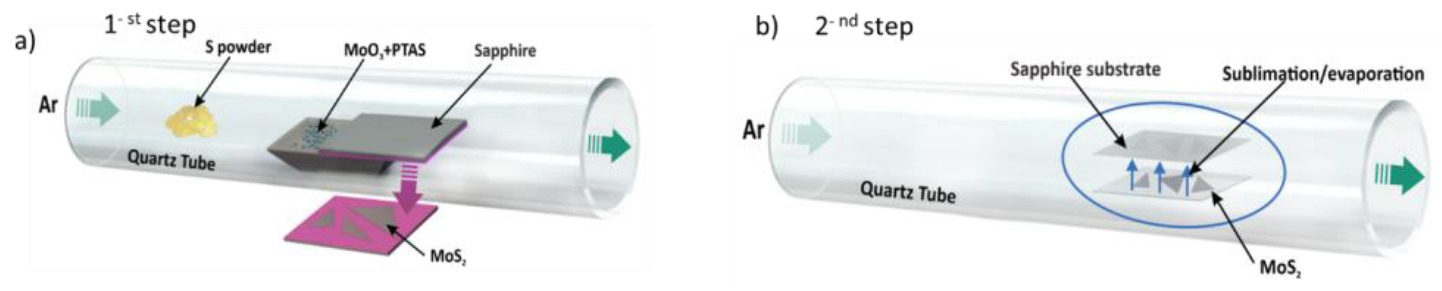
2. Materials and Methods
3. Results and Discussions
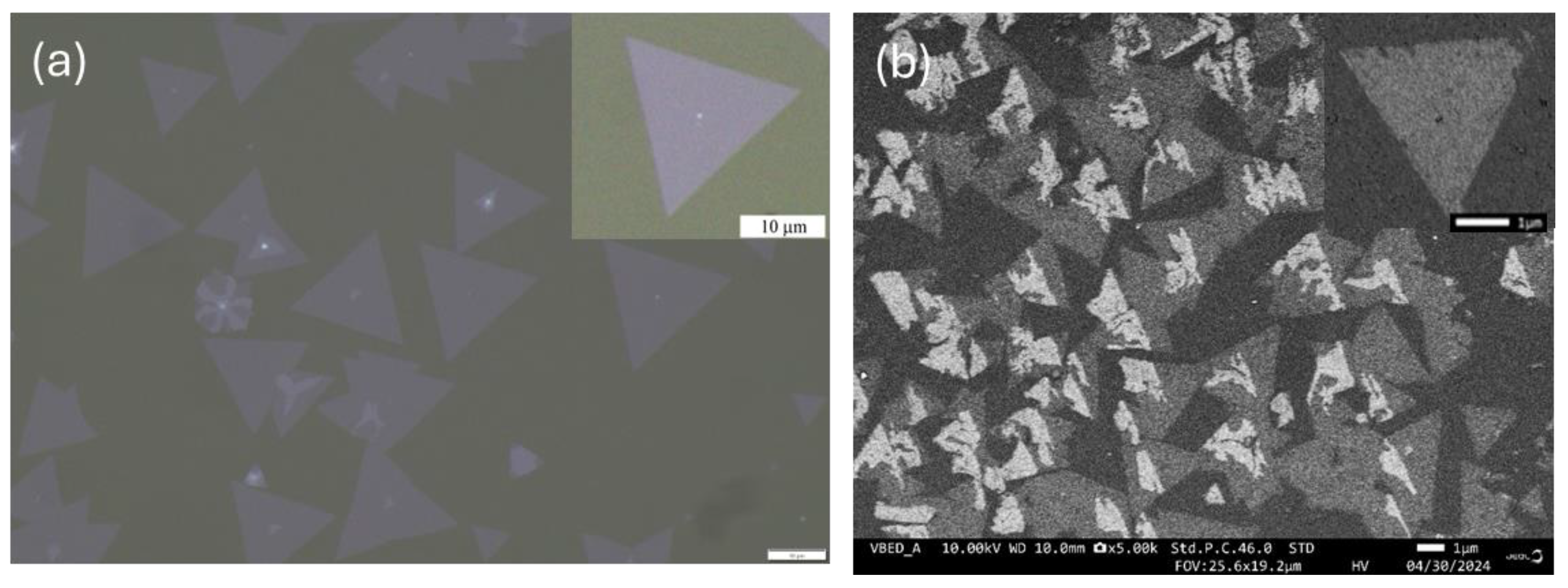
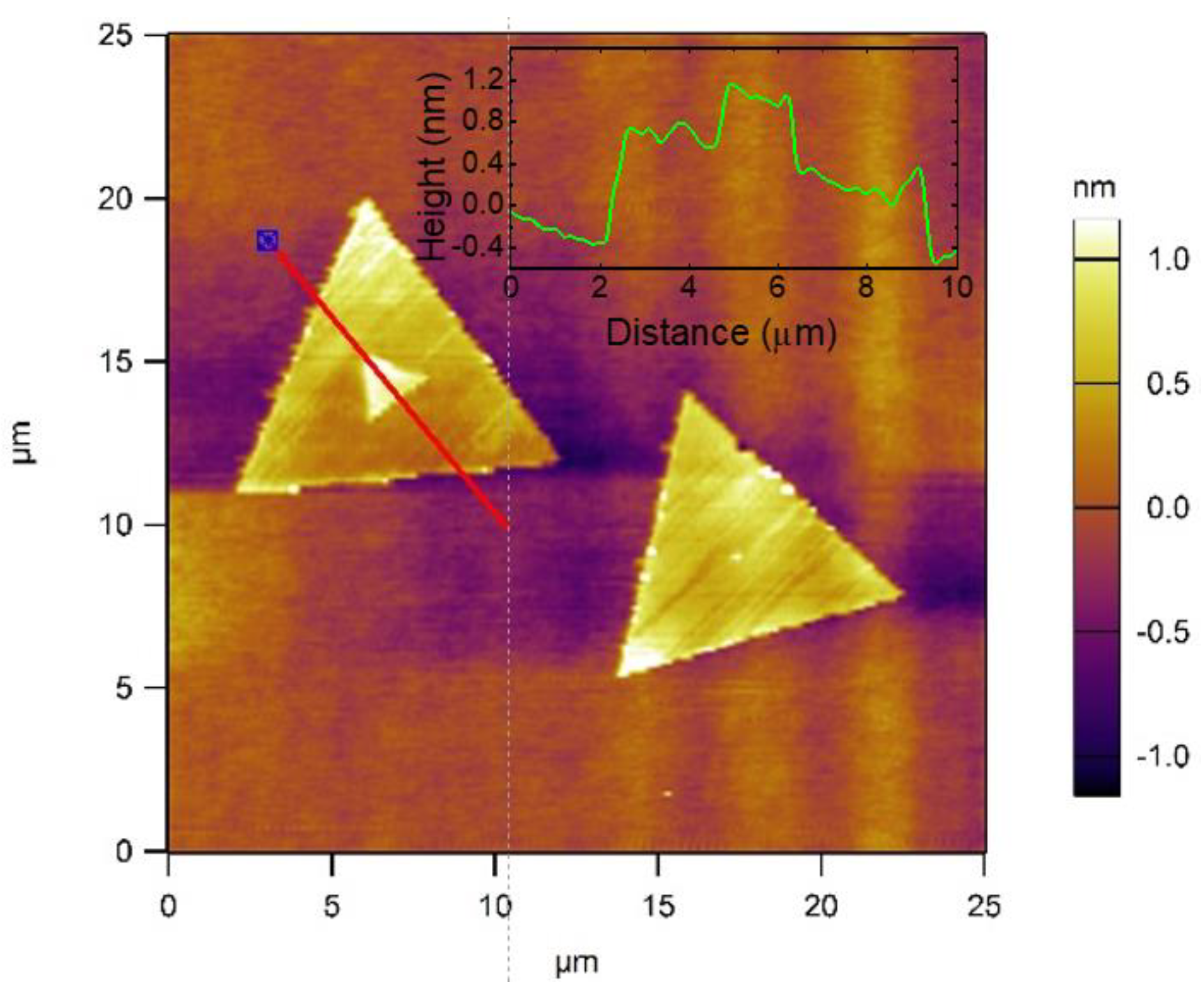
3.1. Optical, SEM and AFM Images and Surface Morphology
3.2. Transmission Electron Microscopy (TEM) Analysis
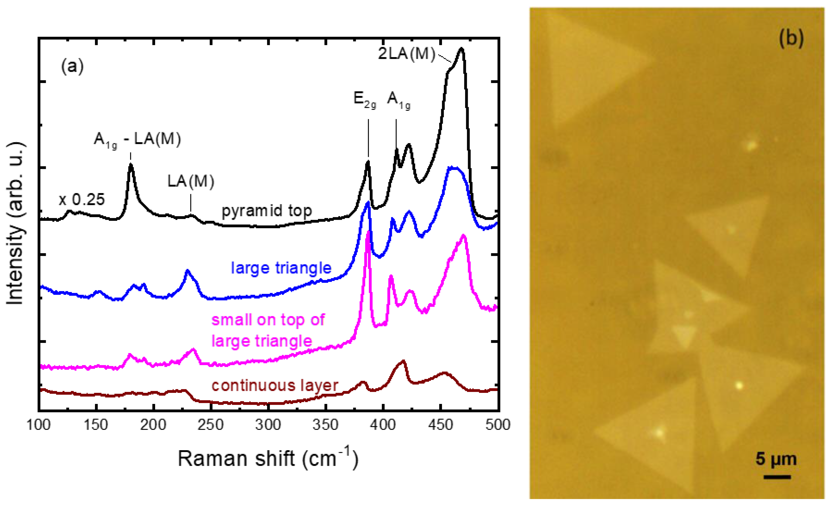
3.3. Raman Analysis
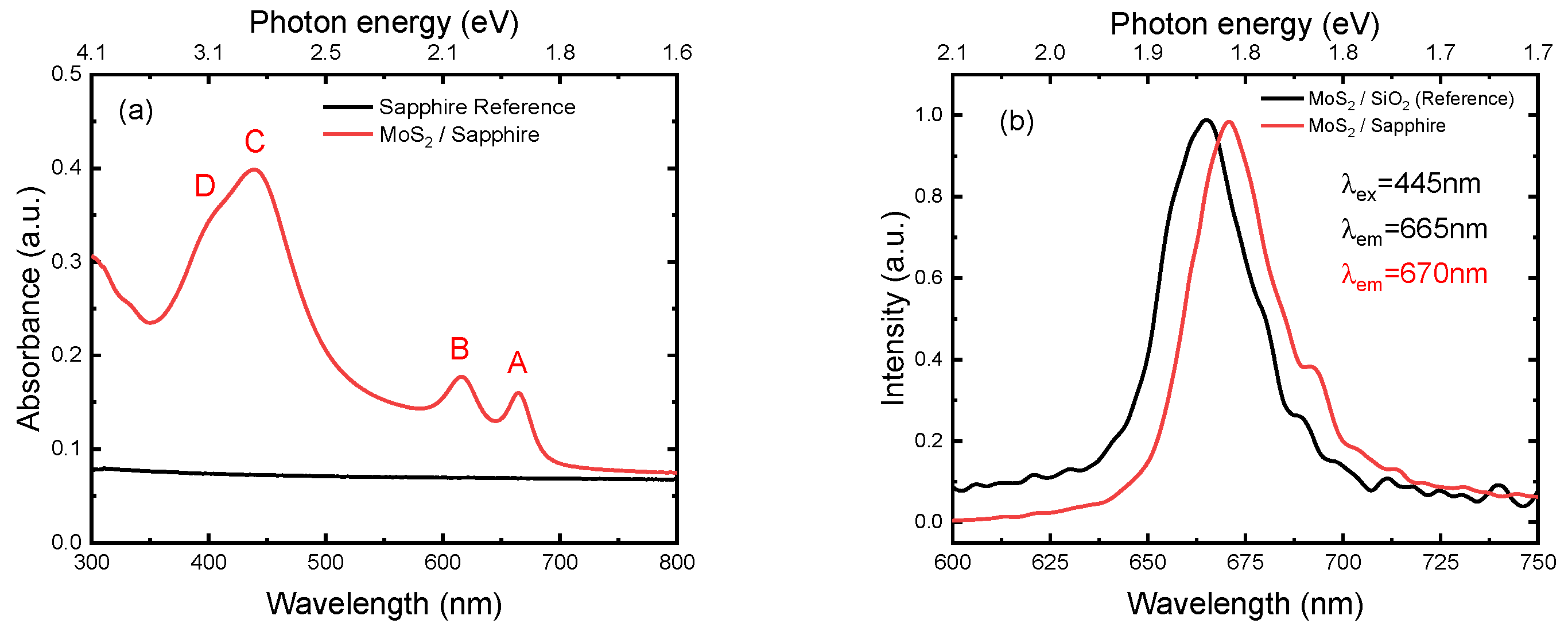
3.4. Optical Absorbance and Photoluminescence
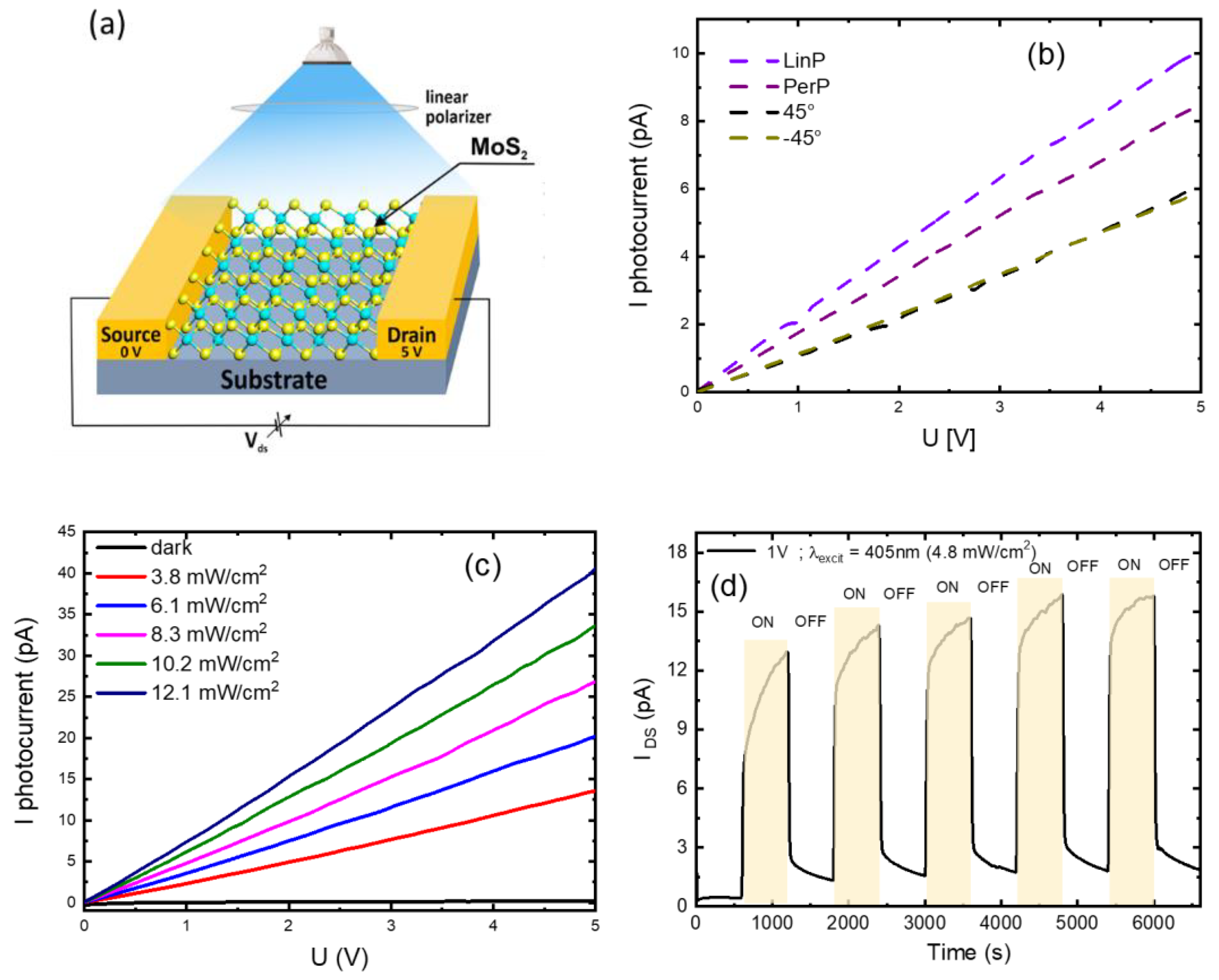
3.5. MoS2-Based Photoresistor
4. Conclusions
Author Contributions
Funding
Data Availability Statement
Conflicts of Interest
References
- Quereda, J.; Rubio-Bollinger, G.; Agraït, N.; Castellanos-Gomez, A. Mechanical Properties and Electric Field Screening of Atomically Thin MoS2 Crystals. In MoS2; Springer: Cham, Switzerland, 2014; pp. 129–153. [Google Scholar]
- Krishnan, U.; Kaur, M.; Singh, K.; Kumar, M.; Kumar, A. A Synoptic Review of MoS2: Synthesis to Applications. Superlattices Microstruct. 2019, 128, 274–297. [Google Scholar] [CrossRef]
- Wang, Z.; Mi, B. Environmental Applications of 2D Molybdenum Disulfide (MoS2) Nanosheets. Environ. Sci. Technol. 2017, 51, 8229–8244. [Google Scholar] [CrossRef]
- Li, X.; Zhu, H. Two-Dimensional MoS2: Properties, Preparation, and Applications. J. Mater. 2015, 1, 33–44. [Google Scholar] [CrossRef]
- Vidya, C.; Manjunatha, C.; Pranjal, A.; Faraaz, I.; Prashantha, K. A Multifunctional Nanostructured Molybdenum Disulphide (MoS2): An Overview on Synthesis, Structural Features, and Potential Applications. Mater. Res. Innov. 2023, 27, 177–193. [Google Scholar] [CrossRef]
- Gołasa, K.; Grzeszczyk, M.; Korona, K.P.; Bozek, R.; Binder, J.; Szczytko, J.; Wysmołek, A.; Babiński, A. Optical Properties of Molybdenum Disulfide (MoS2). Acta Phys. Pol. A 2013, 124, 849–851. [Google Scholar] [CrossRef]
- Ghosh, S.; Withanage, S.S.; Chamlagain, B.; Khondaker, S.I.; Harish, S.; Saha, B.B. Low Pressure Sulfurization and Characterization of Multilayer MoS2 for Potential Applications in Supercapacitors. Energy 2020, 203, 117918. [Google Scholar] [CrossRef]
- Li, N.; Wang, Q.; Shen, C.; Wei, Z.; Yu, H.; Zhao, J.; Lu, X.; Wang, G.; He, C.; Xie, L.; et al. Large-Scale Flexible and Transparent Electronics Based on Monolayer Molybdenum Disulfide Field-Effect Transistors. Nat. Electron. 2020, 3, 711–717. [Google Scholar] [CrossRef]
- Wang, H.; Yu, L.; Lee, Y.H.; Shi, Y.; Hsu, A.; Chin, M.L.; Li, L.J.; Dubey, M.; Kong, J.; Palacios, T. Integrated Circuits Based on Bilayer MoS2 Transistors. Nano Lett. 2012, 12, 4674–4680. [Google Scholar] [CrossRef]
- Li, Z.; Wu, J.; Wang, C.; Zhang, H.; Yu, W.; Lu, Y.; Liu, X. High-Performance Monolayer MoS2 photodetector Enabled by Oxide Stress Liner Using Scalable Chemical Vapor Growth Method. Nanophotonics 2020, 9, 1981–1991. [Google Scholar] [CrossRef]
- Radisavljevic, B.; Radenovic, A.; Brivio, J.; Giacometti, V.; Kis, A. Single-Layer MoS2 Transistors. Nat. Nanotechnol. 2011, 6, 147–150. [Google Scholar] [CrossRef]
- Kim, S.; Konar, A.; Hwang, W.S.; Lee, J.H.; Lee, J.; Yang, J.; Jung, C.; Kim, H.; Yoo, J.B.; Choi, J.Y.; et al. High-Mobility and Low-Power Thin-Film Transistors Based on Multilayer MoS2 Crystals. Nat. Commun. 2012, 3, 1011. [Google Scholar] [CrossRef]
- Huang, Z.; Han, W.; Tang, H.; Ren, L.; Chander, D.S.; Qi, X.; Zhang, H. Photoelectrochemical-Type Sunlight Photodetector Based on MoS2/Graphene Heterostructure. 2d Mater. 2015, 2, 035011. [Google Scholar] [CrossRef]
- Ye, Z.; Tan, C.; Huang, X.; Ouyang, Y.; Yang, L.; Wang, Z.; Dong, M. Emerging MoS2 Wafer-Scale Technique for Integrated Circuits. Nanomicro Lett. 2023, 15, 38. [Google Scholar] [CrossRef]
- Jeon, J.; Jang, S.K.; Jeon, S.M.; Yoo, G.; Jang, Y.H.; Park, J.H.; Lee, S. Layer-Controlled CVD Growth of Large-Area Two-Dimensional MoS2 Films. Nanoscale 2015, 7, 1688–1695. [Google Scholar] [CrossRef]
- Yu, Y.; Li, C.; Liu, Y.; Su, L.; Zhang, Y.; Cao, L. Controlled Scalable Synthesis of Uniform, High-Quality Monolayer and Few-Layer MoS2 Films. Sci. Rep. 2013, 3, 1866. [Google Scholar] [CrossRef]
- Li, H.; Wu, J.; Yin, Z.; Zhang, H. Preparation and Applications of Mechanically Exfoliated Single-Layer and Multilayer MoS2 and WSe2 Nanosheets. Acc. Chem. Res. 2014, 47, 1067–1075. [Google Scholar] [CrossRef]
- Ottaviano, L.; Palleschi, S.; Perrozzi, F.; D’Olimpio, G.; Priante, F.; Donarelli, M.; Benassi, P.; Nardone, M.; Gonchigsuren, M.; Gombosuren, M.; et al. Mechanical Exfoliation and Layer Number Identification of MoS2 Revisited. 2d Mater. 2017, 4, 045013. [Google Scholar] [CrossRef]
- Wu, C.; Luo, S.; Luo, X.; Weng, J.; Shang, C.; Liu, Z.; Zhao, H.; Sawtell, D.; Xiong, L. Exploring the Photoelectric Properties of 2D MoS2 Thin Films Grown by CVD. J. Mater. Res. 2022, 37, 3470–3480. [Google Scholar] [CrossRef]
- Nguyen, V.T.; Nguyen, V.C.; Tran, V.H.; Park, J.-Y. Growth of Bilayer MoS2 Flakes by Reverse Flow Chemical Vapor Deposition. Mater. Lett. 2023, 346, 134553. [Google Scholar] [CrossRef]
- Napoleonov, B.; Petrova, D.; Rafailov, P.; Videva, V.; Strijkova, V.; Karashanova, D.; Dimitrov, D.; Marinova, V. Growth of 2D MoS2 on Sapphire and Mica. J. Phys. Conf. Ser. 2024, 2710, 012016. [Google Scholar] [CrossRef]
- Chen, F.; Su, W.; Zhao, S.; Lv, Y.; Ding, S.; Fu, L. Morphological Evolution of Atomically Thin MoS2 flakes Synthesized by a Chemical Vapor Deposition Strategy. CrystEngComm 2020, 22, 4174–4179. [Google Scholar] [CrossRef]
- Tan, L.K.; Liu, B.; Teng, J.H.; Guo, S.; Low, H.Y.; Loh, K.P. Atomic Layer Deposition of a MoS2 Film. Nanoscale 2014, 6, 10584–10588. [Google Scholar] [CrossRef] [PubMed]
- Liu, Y.; Nan, H.; Wu, X.; Pan, W.; Wang, W.; Bai, J.; Zhao, W.; Sun, L.; Wang, X.; Ni, Z. Layer-by-Layer Thinning of MoS2 by Plasma. ACS Nano 2013, 7, 4202–4209. [Google Scholar] [CrossRef] [PubMed]
- Ma, X.; Shi, M. Thermal Evaporation Deposition of Few-Layer MoS2 Films. Nanomicro Lett. 2013, 5, 135–139. [Google Scholar] [CrossRef]
- Yang, K.Y.; Nguyen, H.T.; Tsao, Y.M.; Artemkina, S.B.; Fedorov, V.E.; Huang, C.W.; Wang, H.C. Large Area MoS2 Thin Film Growth by Direct Sulfurization. Sci. Rep. 2023, 13, 8378. [Google Scholar] [CrossRef] [PubMed]
- Ko, H.; Kim, H.S.; Ramzan, M.S.; Byeon, S.; Choi, S.H.; Kim, K.K.; Kim, Y.H.; Kim, S.M. Atomistic Mechanisms of Seeding Promoter-Controlled Growth of Molybdenum Disulphide. 2d Mater. 2020, 7, 015013. [Google Scholar] [CrossRef]
- Choi, H.J.; Jung, Y.S.; Lee, S.M.; Kang, S.; Seo, D.; Kim, H.; Choi, H.J.; Lee, G.H.; Cho, Y.S. Large-Scale Self-Limiting Synthesis of Monolayer MoS2 via Proximity Evaporation from Mo Films. Cryst. Growth Des. 2020, 20, 2698–2705. [Google Scholar] [CrossRef]
- Yu, C.; Chang, P.; Guan, L.; Tao, J. Inward Growth of Monolayer MoS2 Single Crystals from Molten Na2MoO4 Droplets. Mater. Chem. Phys. 2020, 240, 122203. [Google Scholar] [CrossRef]
- O’Brien, M.; McEvoy, N.; Hallam, T.; Kim, H.Y.; Berner, N.C.; Hanlon, D.; Lee, K.; Coleman, J.N.; Duesberg, G.S. Transition Metal Dichalcogenide Growth via Close Proximity Precursor Supply. Sci. Rep. 2014, 4, 7374. [Google Scholar] [CrossRef]
- Lee, Y.H.; Yu, L.; Wang, H.; Fang, W.; Ling, X.; Shi, Y.; Lin, C.T.; Huang, J.K.; Chang, M.T.; Chang, C.S.; et al. Synthesis and Transfer of Single-Layer Transition Metal Disulfides on Diverse Surfaces. Nano Lett. 2013, 13, 1852–1857. [Google Scholar] [CrossRef]
- Lee, C.; Yan, H.; Brus, L.E.; Heinz, T.F.; Hone, J.; Ryu, S. Anomalous Lattice Vibrations of Single- and Few-Layer MoS2. ACS Nano 2010, 4, 2695–2700. [Google Scholar] [CrossRef] [PubMed]
- Cullen, C.P.; Hartwig, O.; Coileáin, C.Ó.; Mcmanus, J.B.; Peters, L.; Ilhan, C.; Duesberg, G.S.; Mcevoy, N. Synthesis and Thermal Stability of TMD Thin Films: A Comprehensive XPS and Raman Study. arXiv 2021, arXiv:2106.07366. [Google Scholar]
- Li, H.; Zhang, Q.; Yap, C.C.R.; Tay, B.K.; Edwin, T.H.T.; Olivier, A.; Baillargeat, D. From Bulk to Monolayer MoS2: Evolution of Raman Scattering. Adv. Funct. Mater. 2012, 22, 1385–1390. [Google Scholar] [CrossRef]
- Lee, J.U.; Park, J.; Son, Y.W.; Cheong, H. Anomalous Excitonic Resonance Raman Effects in Few-Layered MoS2. Nanoscale 2015, 7, 3229–3236. [Google Scholar] [CrossRef] [PubMed]
- Houssa, M.; Dimoulas, A.; Molle, A. (Eds.) 2D Materials for Nanoelectronics; CRC Press: Boca Raton, FL, USA, 2016; ISBN 9780429194559. [Google Scholar]
- Golovynskyi, S.; Irfan, I.; Bosi, M.; Seravalli, L.; Datsenko, O.I.; Golovynska, I.; Li, B.; Lin, D.; Qu, J. Exciton and Trion in Few-Layer MoS2: Thickness- and Temperature-Dependent Photoluminescence. Appl. Surf. Sci. 2020, 515, 146033. [Google Scholar] [CrossRef]
- Wang, Q.H.; Kalantar-Zadeh, K.; Kis, A.; Coleman, J.N.; Strano, M.S. Electronics and Optoelectronics of Two-Dimensional Transition Metal Dichalcogenides. Nat. Nanotechnol. 2012, 7, 699–712. [Google Scholar] [CrossRef] [PubMed]
- Tummala, P.; Lamperti, A.; Alia, M.; Kozma, E.; Nobili, L.G.; Molle, A. Application-Oriented Growth of a Molybdenum Disulfide (MoS2) Single Layer by Means of Parametrically Optimized Chemical Vapor Deposition. Materials 2020, 13, 2786. [Google Scholar] [CrossRef] [PubMed]
- Wang, K.; Wang, J.; Fan, J.; Lotya, M.; O’Neill, A.; Fox, D.; Feng, Y.; Zhang, X.; Jiang, B.; Zhao, Q.; et al. Ultrafast Saturable Absorption of Two-Dimensional MoS2 Nanosheets. ACS Nano 2013, 7, 9260–9267. [Google Scholar] [CrossRef]
- Splendiani, A.; Sun, L.; Zhang, Y.; Li, T.; Kim, J.; Chim, C.Y.; Galli, G.; Wang, F. Emerging Photoluminescence in Monolayer MoS2. Nano Lett. 2010, 10, 1271–1275. [Google Scholar] [CrossRef]
- Eda, G.; Yamaguchi, H.; Voiry, D.; Fujita, T.; Chen, M.; Chhowalla, M. Photoluminescence from Chemically Exfoliated MoS2. Nano Lett. 2011, 11, 5111–5116. [Google Scholar] [CrossRef]
- Xing, X.; Zhao, L.; Zhang, Z.; Lin, X.; Yu, Y.; Jin, Z.; Liu, W.; Zhang, W.; Ma, G. The Modulation of Terahertz Photoconductivity in CVD Grown N-Doped Monolayer MoS2 with Gas Adsorption. J. Phys. Condens. Matter 2019, 21, 245001. [Google Scholar] [CrossRef]
- Castellanos-Gomez, A.; Quereda, J.; Van Der Meulen, H.P.; Agraït, N.; Rubio-Bollinger, G. Spatially Resolved Optical Absorption Spectroscopy of Single- and Few-Layer MoS2 by Hyperspectral Imaging. Nanotechnology 2016, 27, 115705. [Google Scholar] [CrossRef]
- Zhang, W.; Huang, J.K.; Chen, C.H.; Chang, Y.H.; Cheng, Y.J.; Li, L.J. High-Gain Phototransistors Based on a CVD MoS2 Monolayer. Adv. Mater. 2013, 25, 3456–3461. [Google Scholar] [CrossRef] [PubMed]
- Minn, K.; Anopchenko, A.; Chang, C.W.; Mishra, R.; Kim, J.; Zhang, Z.; Lu, Y.J.; Gwo, S.; Lee, H.W.H. Enhanced Spontaneous Emission of Monolayer MoS2 on Epitaxially Grown Titanium Nitride Epsilon-Near-Zero Thin Films. Nano Lett. 2021, 21, 4928–4936. [Google Scholar] [CrossRef]
- Mouri, S.; Miyauchi, Y.; Matsuda, K. Tunable Photoluminescence of Monolayer MoS2 via Chemical Doping. Nano Lett. 2013, 13, 5944–5948. [Google Scholar] [CrossRef]
- Li, Z.; Chang, S.W.; Chen, C.C.; Cronin, S.B. Enhanced Photocurrent and Photoluminescence Spectra in MoS2 under Ionic Liquid Gating. Nano Res. 2014, 7, 973–980. [Google Scholar] [CrossRef]
- Buscema, M.; Island, J.O.; Groenendijk, D.J.; Blanter, S.I.; Steele, G.A.; Van Der Zant, H.S.J.; Castellanos-Gomez, A. Photocurrent Generation with Two-Dimensional van Der Waals Semiconductors. Chem. Soc. Rev. 2015, 44, 3691–3718. [Google Scholar] [CrossRef] [PubMed]
- Li, J.; Yu, W.; Chu, S.; Yang, H.; Shi, K.; Gong, Q. Polarization-Dependent Photocurrent in MoS2 Phototransistor. In Proceedings of the Physics and Simulation of Optoelectronic Devices XXIII, San Francisco, CA, USA, 7–12 February 2015; Volume 9357, p. 93571F. [Google Scholar]
- Tan, J.; Nan, H.; Fu, Q.; Zhang, X.; Liu, X.; Ni, Z.; Ostrikov, K.; Xiao, S.; Gu, X. Fourfold Polarization-Sensitive Photodetector Based on GaTe/MoS2 van Der Waals Heterojunction. Adv. Electron. Mater. 2022, 8, 2100673. [Google Scholar] [CrossRef]
- Wei, Z.; Zheng, X.; Wei, Y.; Zhang, X.; Luo, W.; Liu, J.; Peng, G.; Huang, H.; Lv, T.; Zhang, X.; et al. Van Der Waals Interlayer Coupling Induces Distinct Linear Dichroism in WSe2 Photodetectors. Adv. Opt. Mater. 2023, 11, 2201962. [Google Scholar] [CrossRef]
- Aji, A.S.; Nishi, R.; Ago, H.; Ohno, Y. High Output Voltage Generation of over 5 V from Liquid Motion on Single-Layer MoS2. Nano Energy 2020, 68, 104370. [Google Scholar] [CrossRef]
- Lu, J.; Ye, Q.; Ma, C.; Zheng, Z.; Yao, J.; Yang, G. Dielectric Contrast Tailoring for Polarized Photosensitivity toward Multiplexing Optical Communications and Dynamic Encrypt Technology. ACS Nano 2022, 16, 12852–12865. [Google Scholar] [CrossRef] [PubMed]

Disclaimer/Publisher’s Note: The statements, opinions and data contained in all publications are solely those of the individual author(s) and contributor(s) and not of MDPI and/or the editor(s). MDPI and/or the editor(s) disclaim responsibility for any injury to people or property resulting from any ideas, methods, instructions or products referred to in the content. |
© 2024 by the authors. Licensee MDPI, Basel, Switzerland. This article is an open access article distributed under the terms and conditions of the Creative Commons Attribution (CC BY) license (https://creativecommons.org/licenses/by/4.0/).
Share and Cite
Napoleonov, B.; Petrova, D.; Minev, N.; Rafailov, P.; Videva, V.; Karashanova, D.; Ranguelov, B.; Atanasova-Vladimirova, S.; Strijkova, V.; Dimov, D.; et al. Growth of Monolayer MoS2 Flakes via Close Proximity Re-Evaporation. Nanomaterials 2024, 14, 1213. https://doi.org/10.3390/nano14141213
Napoleonov B, Petrova D, Minev N, Rafailov P, Videva V, Karashanova D, Ranguelov B, Atanasova-Vladimirova S, Strijkova V, Dimov D, et al. Growth of Monolayer MoS2 Flakes via Close Proximity Re-Evaporation. Nanomaterials. 2024; 14(14):1213. https://doi.org/10.3390/nano14141213
Chicago/Turabian StyleNapoleonov, Blagovest, Dimitrina Petrova, Nikolay Minev, Peter Rafailov, Vladimira Videva, Daniela Karashanova, Bogdan Ranguelov, Stela Atanasova-Vladimirova, Velichka Strijkova, Deyan Dimov, and et al. 2024. "Growth of Monolayer MoS2 Flakes via Close Proximity Re-Evaporation" Nanomaterials 14, no. 14: 1213. https://doi.org/10.3390/nano14141213
APA StyleNapoleonov, B., Petrova, D., Minev, N., Rafailov, P., Videva, V., Karashanova, D., Ranguelov, B., Atanasova-Vladimirova, S., Strijkova, V., Dimov, D., Dimitrov, D., & Marinova, V. (2024). Growth of Monolayer MoS2 Flakes via Close Proximity Re-Evaporation. Nanomaterials, 14(14), 1213. https://doi.org/10.3390/nano14141213