
Area-Selective Atomic Layer Deposition of Ru Using Carbonyl-Based Precursor and Oxygen Co-Reactant: Understanding Defect Formation Mechanisms

 , , , and
Abstract
1. Introduction
2. Materials and Methods
3. Results & Discussion
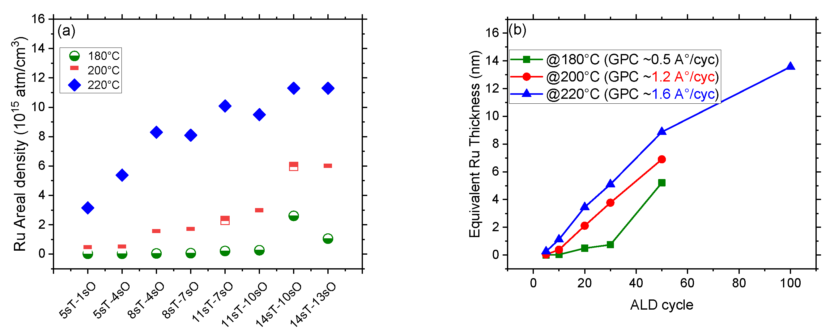
3.1. ALD of Ruthenium
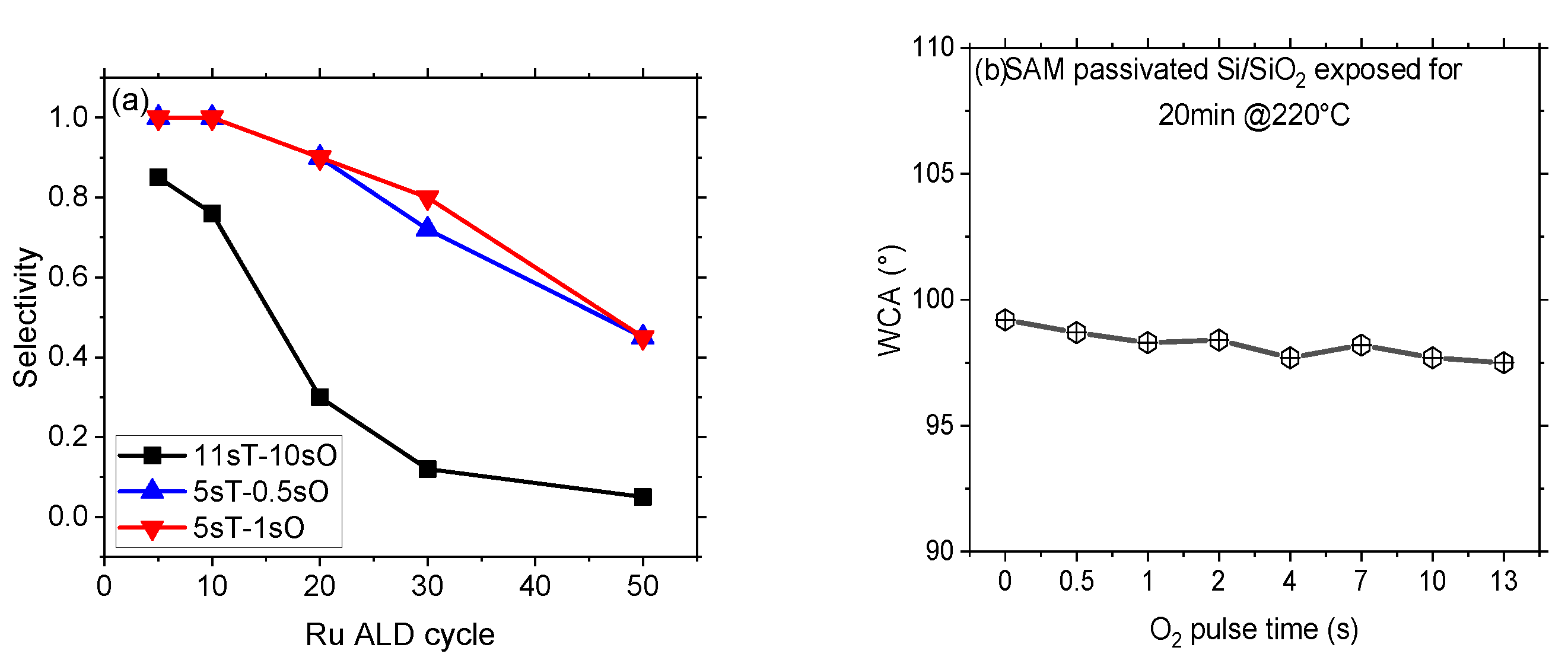
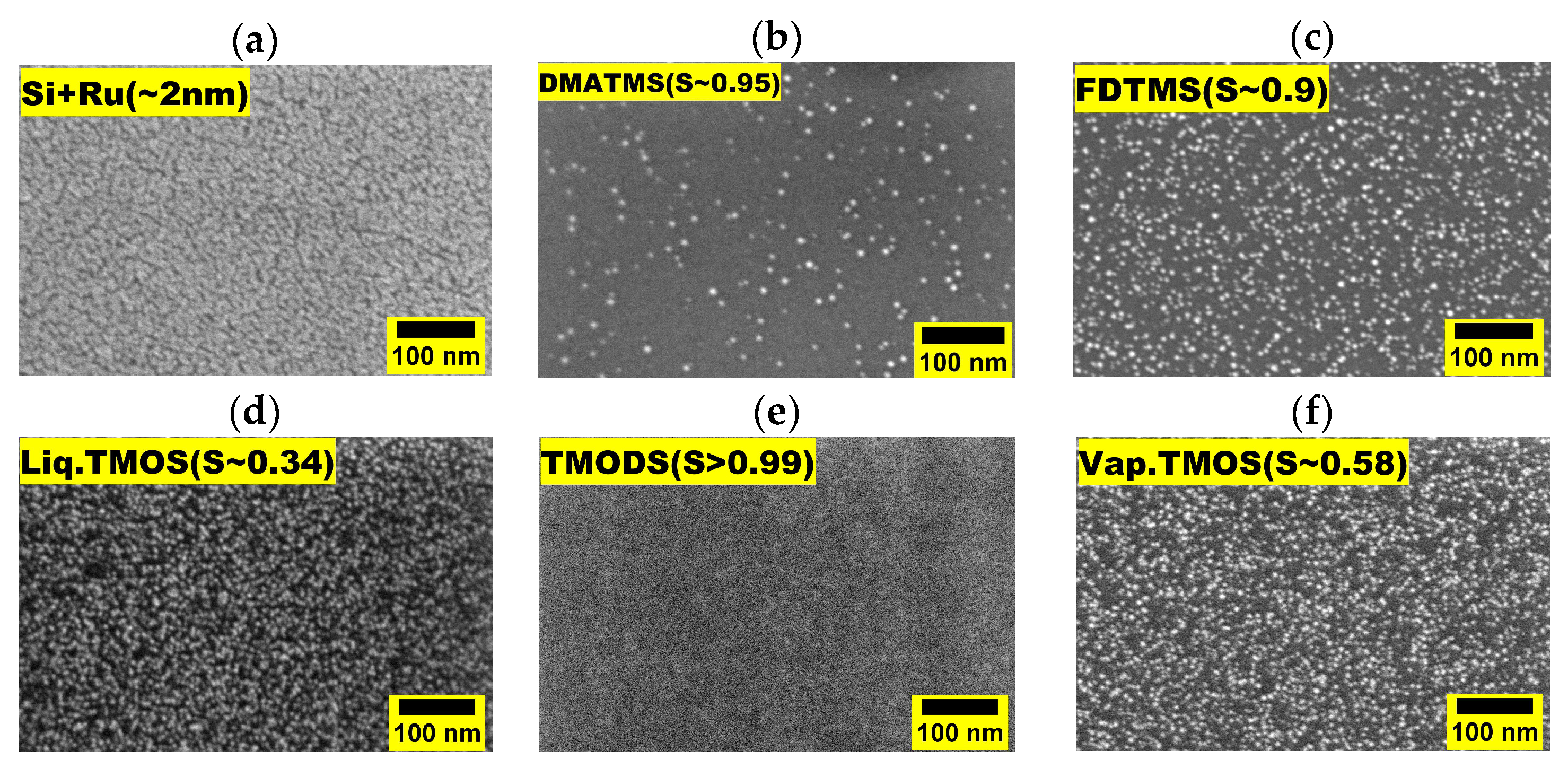
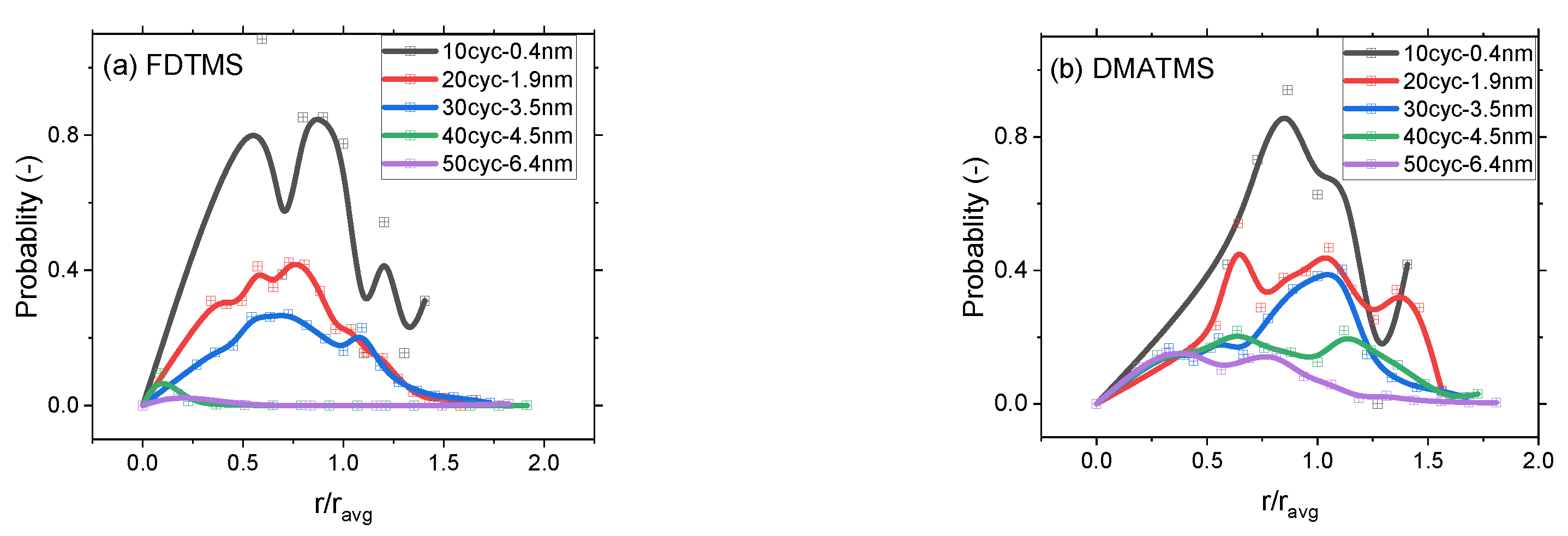
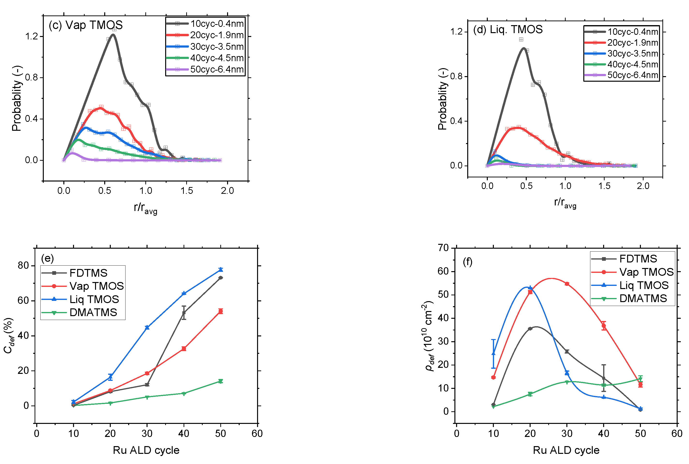
3.2. Selectivity and Defect Analysis
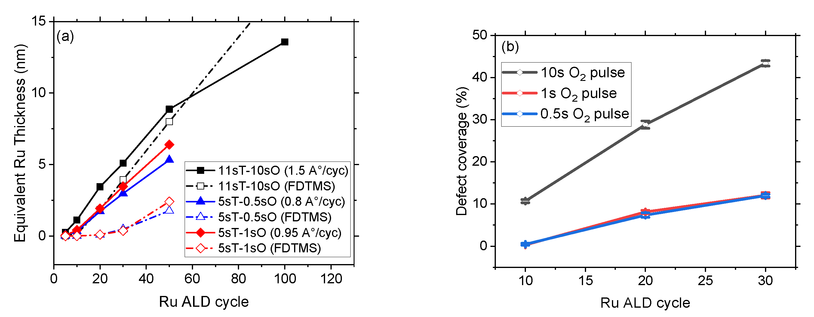
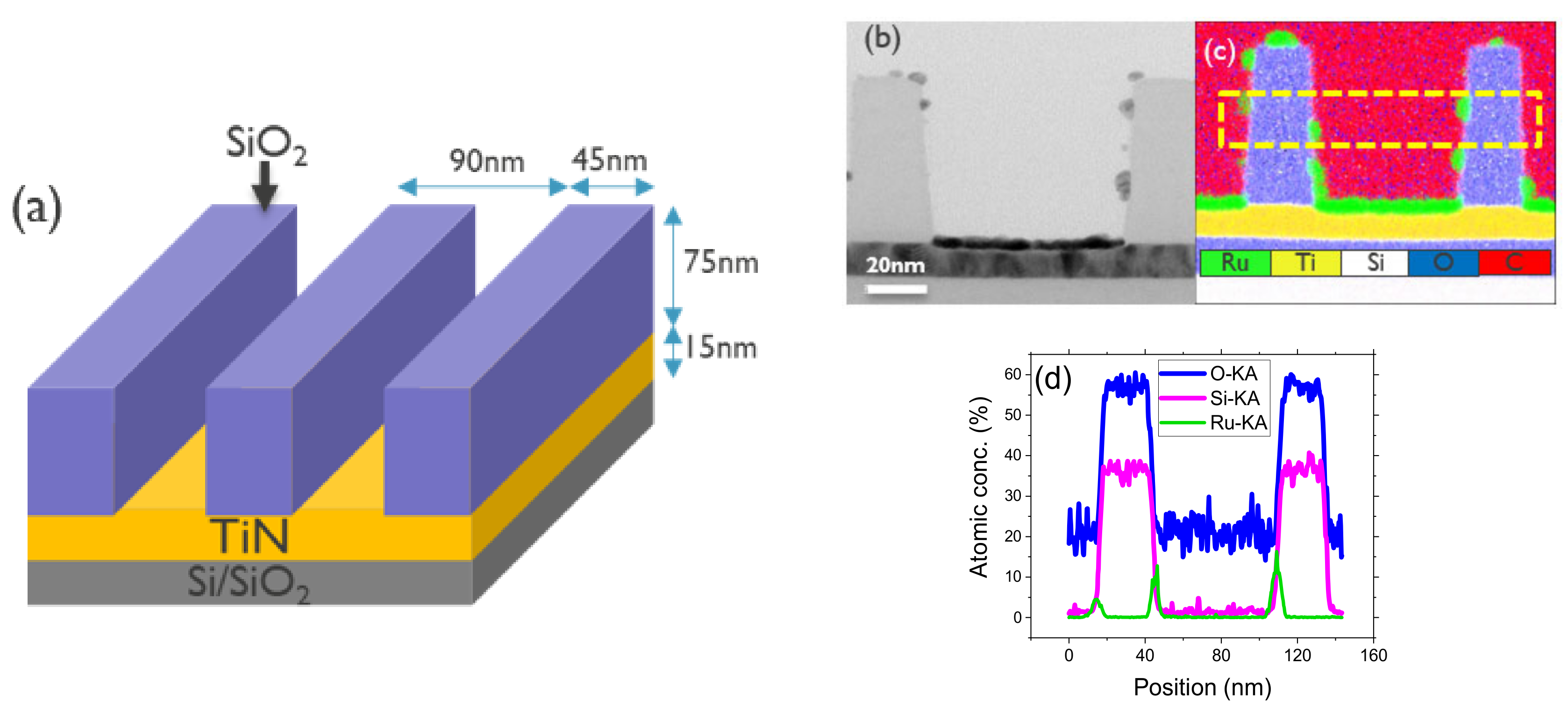
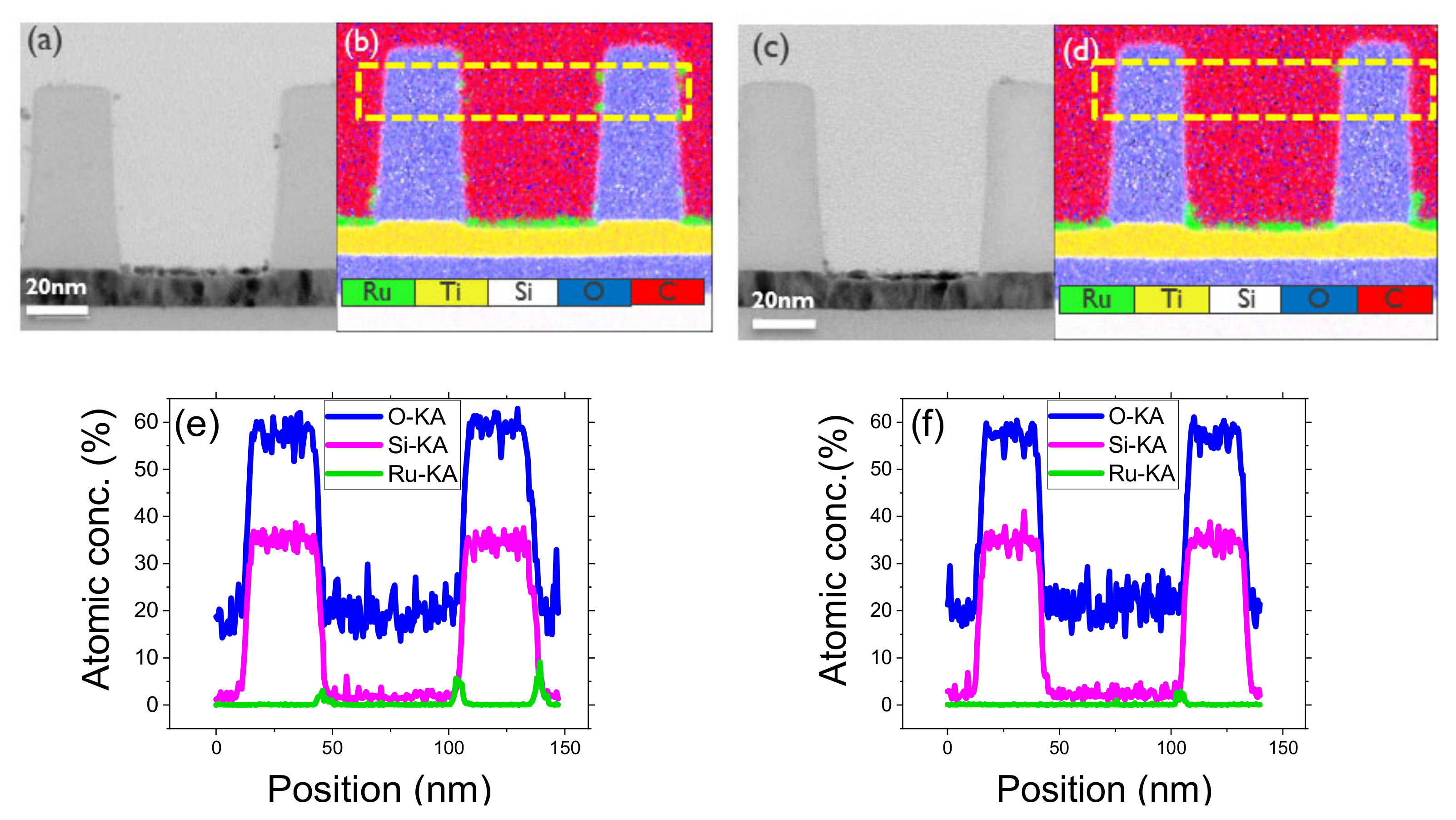
3.3. ASD of Ru on SiO2/TiN Pattern
4. Conclusions
Supplementary Materials
Author Contributions
Funding
Data Availability Statement
Acknowledgments
Conflicts of Interest
References
- Parsons, G.N.; Clark, R.D. Area-Selective Deposition: Fundamentals, Applications, and Future Outlook. Chem. Mater. 2020, 32, 4920–4953. [Google Scholar] [CrossRef]
- Schaller, R.R. Moore’s Law: Past, Present and Future. IEEE Spectrum. 1997, 34, 52–59. [Google Scholar] [CrossRef]
- Mackus, A.J.M.; Merkx, M.J.M.; Kessels, W.M.M. From the Bottom-up: Toward Area-Selective Atomic Layer Deposition with High Selectivity. Chem. Mater. 2019, 31, 2–12. [Google Scholar] [CrossRef]
- Lee, J.-M.; Lee, J.; Oh, H.; Kim, J.; Shong, B.; Park, T.J.; Kim, W.-H. Inhibitor-Free Area-Selective Atomic Layer Deposition of SiO2 through Chemoselective Adsorption of an Aminodisilane Precursor on Oxide versus Nitride Substrates. Appl. Surf. Sci. 2022, 589, 152939. [Google Scholar] [CrossRef]
- Mulkens, J.; Kubis, M.; Tel, W.; Maslow, M.; Ma, E.; Chou, K.; Liu, X.; Ren, W.; Hu, X.; Wang, F.; et al. Holistic Approach for Overlay and Edge Placement Error to Meet the 5 nm Technology Node Requirements. In Metrology, Inspection, and Process Control for Microlithography XXXII; Adan, O., Ukraintsev, V.A., Eds.; SPIE: San Jose, CA, USA, 2018; p. 55. [Google Scholar]
- Sato, Y.; Huang, S.-C.; Maruyama, K.; Yamazaki, Y. Edge Placement Error Measurement in Lithography Process with Die to Database Algorithm. In Metrology, Inspection, and Process Control for Microlithography XXXIII; Adan, O., Ukraintsev, V.A., Eds.; SPIE: San Jose, CA, USA, 2019; p. 12. [Google Scholar]
- Mack, C.A.; Adel, M. Overlay and Edge Placement Error Metrology in the Era of Stochastics. In Metrology, Inspection, and Process Control XXXVII; Robinson, J.C., Sendelbach, M.J., Eds.; SPIE: San Jose, CA, USA, 2023; p. 7. [Google Scholar]
- Wolfsteller, A.; Geyer, N.; Nguyen-Duc, T.-K.; Das Kanungo, P.; Zakharov, N.D.; Reiche, M.; Erfurth, W.; Blumtritt, H.; Kalem, S.; Werner, P.; et al. Comparison of the Top-down and Bottom-up Approach to Fabricate Nanowire-Based Silicon/Germanium Heterostructures. Thin Solid Film. 2010, 518, 2555–2561. [Google Scholar] [CrossRef]
- Lee, J.; Lee, J.-M.; Oh, H.; Kim, C.; Kim, J.; Kim, D.H.; Shong, B.; Park, T.J.; Kim, W.-H. Inherently Area-Selective Atomic Layer Deposition of SiO2 Thin Films to Confer Oxide Versus Nitride Selectivity. Adv. Funct. Mater. 2021, 31, 2102556. [Google Scholar] [CrossRef]
- Atanasov, S.E.; Kalanyan, B.; Parsons, G.N. Inherent Substrate-Dependent Growth Initiation and Selective-Area Atomic Layer Deposition of TiO2 Using “Water-Free” Metal-Halide/Metal Alkoxide Reactants. J. Vacuum Sci. Technol. A Vacuum Surf. Film. 2016, 34, 01A148. [Google Scholar] [CrossRef]
- Methaapanon, R.; Bent, S.F. Comparative Study of Titanium Dioxide Atomic Layer Deposition on Silicon Dioxide and Hydrogen-Terminated Silicon. J. Phys. Chem. C 2010, 114, 10498–10504. [Google Scholar] [CrossRef]
- Li, Y.-C.; Cao, K.; Lan, Y.-X.; Zhang, J.-M.; Gong, M.; Wen, Y.-W.; Shan, B.; Chen, R. Inherently Area-Selective Atomic Layer Deposition of Manganese Oxide through Electronegativity-Induced Adsorption. Molecules 2021, 26, 3056. [Google Scholar] [CrossRef]
- Nye, R.A.; Van Dongen, K.; De Simone, D.; Oka, H.; Parsons, G.N.; Delabie, A. Enhancing Performance and Function of Polymethacrylate Extreme Ultraviolet Resists Using Area-Selective Deposition. Chem. Mater. 2023, 35, 2016–2026. [Google Scholar] [CrossRef]
- Haider, A.; Deminskyi, P.; Khan, T.M.; Eren, H.; Biyikli, N. Area-Selective Atomic Layer Deposition Using an Inductively Coupled Plasma Polymerized Fluorocarbon Layer: A Case Study for Metal Oxides. J. Phys. Chem. C 2016, 120, 26393–26401. [Google Scholar] [CrossRef]
- Poonkottil, N.; Rijckaert, H.; Rajendran, K.; Petit, R.R.; Martin, L.I.D.J.; Van Thourhout, D.; Van Driessche, I.; Detavernier, C.; Dendooven, J. Low Temperature Area Selective Atomic Layer Deposition of Ruthenium Dioxide Thin Films Using Polymers as Inhibition Layers. Adv. Mater. Interfaces 2023, 10, 2201934. [Google Scholar] [CrossRef]
- Kim, Y.R.; Jeon, I.S.; Yim, S.; Lee, A.H.; Kim, S.; Kim, M.; Sohn, E.-H.; Song, W.; Jung, H.-K.; Lee, S.S.; et al. Fluorine-Containing Polymeric Inhibitor for Highly Selective and Durable Area-Selective Atomic Layer Deposition. Appl. Surf. Sci. 2022, 578, 152056. [Google Scholar] [CrossRef]
- Pasquali, M.; Brady-Boyd, A.; Leśniewska, A.; Carolan, P.; Conard, T.; O’Connor, R.; De Gendt, S.; Armini, S. Area-Selective Deposition of AlOx and Al-Silicate for Fully Self-Aligned via Integration. ACS Appl. Mater. Interfaces 2023, 15, 6079–6091. [Google Scholar] [CrossRef] [PubMed]
- Lodha, J.K.; Pollentier, I.; Conard, T.; Vallat, R.; De Gendt, S.; Armini, S. Self-Assembled Monolayers as Inhibitors for Area-Selective Deposition: A Novel Approach towards Resist-Less EUV Lithography. Appl. Surf. Sci. 2022, 606, 154657. [Google Scholar] [CrossRef]
- Hashemi, F.S.M.; Prasittichai, C.; Bent, S.F. A New Resist for Area Selective Atomic and Molecular Layer Deposition on Metal–Dielectric Patterns. J. Phys. Chem. C 2014, 118, 10957–10962. [Google Scholar] [CrossRef]
- Lee, W.; Prinz, F.B. Area-Selective Atomic Layer Deposition Using Self-Assembled Monolayer and Scanning Probe Lithography. J. Electrochem. Soc. 2009, 156, G125. [Google Scholar] [CrossRef]
- Clerix, J.J.; Warad, L.; Hung, J.; Hody, H.; Van Roey, F.; Lorusso, G.; Koret, R.; Lee, W.T.; Shah, K.; Delabie, A. 300 Mm-Wafer Metrology for Area-Selective Deposition in Nanoscale Patterns: A Case Study for Ruthenium Atomic Layer Deposition. Appl. Surf. Sci. 2023, 626, 157222. [Google Scholar] [CrossRef]
- Mameli, A.; Teplyakov, A.V. Selection Criteria for Small-Molecule Inhibitors in Area-Selective Atomic Layer Deposition: Fundamental Surface Chemistry Considerations. Acc. Chem. Res. 2023, 56, 2084–2095. [Google Scholar] [CrossRef]
- Van Dongen, K.; Nye, R.A.; Clerix, J.-W.J.; Sixt, C.; De Simone, D.; Delabie, A. Aminosilane Small Molecule Inhibitors for Area-Selective Deposition: Study of Substrate-Inhibitor Interfacial Interactions. J. Vacuum Sci. Technol. A 2023, 41, 032404. [Google Scholar] [CrossRef]
- Ulman, A. Formation and Structure of Self-Assembled Monolayers. Chem. Rev. 1996, 96, 1533–1554. [Google Scholar] [CrossRef] [PubMed]
- Schreiber, F. Self-Assembled Monolayers: From Simple Model Systems to Biofunctionalized Interfaces. J. Phys. Condens. Matter 2004, 16, R881–R900. [Google Scholar] [CrossRef]
- Budz, H.A.; LaPierre, R.R. Properties of Octadecanethiol Self-Assembled Monolayers Deposited on GaAs from Liquid and Vapor Phases. J. Vacuum Sci. Technol. A Vacuum Surf. Film. 2008, 26, 1425–1431. [Google Scholar] [CrossRef]
- Lin, K.-Y.; Li, C.; Engelmann, S.; Bruce, R.L.; Joseph, E.A.; Metzler, D.; Oehrlein, G.S. Selective Atomic Layer Etching of HfO2 over Silicon by Precursor and Substrate-Dependent Selective Deposition. J. Vacuum Sci. Technol. A Vacuum Surf. Film. 2020, 38, 032601. [Google Scholar] [CrossRef]
- Soethoudt, J.; Hody, H.; Spampinato, V.; Franquet, A.; Briggs, B.; Chan, B.T.; Delabie, A. Defect Mitigation in Area-Selective Atomic Layer Deposition of Ruthenium on Titanium Nitride/Dielectric Nanopatterns. Adv. Mater. Interfaces 2019, 6, 1900896. [Google Scholar] [CrossRef]
- Kotsugi, Y.; Han, S.-M.; Kim, Y.-H.; Cheon, T.; Nandi, D.K.; Ramesh, R.; Yu, N.-K.; Son, K.; Tsugawa, T.; Ohtake, S.; et al. Atomic Layer Deposition of Ru for Replacing Cu-Interconnects. Chem. Mater. 2021, 33, 5639–5651. [Google Scholar] [CrossRef]
- Lee, J.-M.; Lee, S.-H.; Oh, J.; Kim, W.-H. Area-Selective Atomic Layer Deposition of High-Quality Ru Thin Films by Chemo-Selective Adsorption of Short Alkylating Agents. Mater. Lett. 2023, 333, 133574. [Google Scholar] [CrossRef]
- Lee, S.-H.; Lee, J.-M.; Lee, J.H.; Kwak, J.; Chung, S.-W.; Kim, W.-H. Area-Selective Atomic Layer Deposition of Ru Thin Films Using Phosphonic Acid Self-Assembled Monolayers for Metal/Dielectric Selectivity. Mater. Lett. 2022, 328, 133187. [Google Scholar] [CrossRef]
- Ko, E.C.; Kim, J.Y.; Rhee, H.; Kim, K.M.; Han, J.H. Low-Resistivity Ruthenium Metal Thin Films Grown via Atomic Layer Deposition Using Dicarbonyl-Bis(5-Methyl-2,4-Hexanediketonato)Ruthenium(II) and Oxygen. Mater. Sci. Semicond. Process. 2023, 156, 107258. [Google Scholar] [CrossRef]
- Poonkottil, N.; Minjauw, M.M.; Werbrouck, A.; Checchia, S.; Solano, E.; Nisula, M.; Franquet, A.; Detavernier, C.; Dendooven, J. Atomic Layer Deposition of Ruthenium Dioxide Based on Redox Reactions between Alcohols and Ruthenium Tetroxide. Chem. Mater. 2022, 34, 8946–8958. [Google Scholar] [CrossRef]
- Suh, Y.-S.; Lazar, H.; Chen, B.; Lee, J.-H.; Misra, V. Electrical Characteristics of HfO2 Dielectrics with Ru Metal Gate Electrodes. J. Electrochem. Soc. 2005, 152, F138. [Google Scholar] [CrossRef]
- Kim, S.K.; Kim, W.-D.; Kim, K.-M.; Hwang, C.S.; Jeong, J. High Dielectric Constant TiO2 Thin Films on a Ru Electrode Grown at 250 °C by Atomic-Layer Deposition. Appl. Phys. Lett. 2004, 85, 4112–4114. [Google Scholar] [CrossRef]
- Kwon, O.J.; Cha, S.H.; Kim, J.J. Ruthenium Bottom Electrode Prepared by Electroplating for a High Density DRAM Capacitor. J. Electrochem. Soc. 2004, 151, C127. [Google Scholar] [CrossRef]
- Vos, M.F.J.; Chopra, S.N.; Verheijen, M.A.; Ekerdt, J.G.; Agarwal, S.; Kessels, W.M.M.; Mackus, A.J.M. Area-Selective Deposition of Ruthenium by Combining Atomic Layer Deposition and Selective Etching. Chem. Mater. 2019, 31, 3878–3882. [Google Scholar] [CrossRef]
- Aaltonen, T.; Alén, P.; Ritala, M.; Leskelä, M. Ruthenium Thin Films Grown by Atomic Layer Deposition. Chem. Vapor Depos. 2003, 9, 45–49. [Google Scholar] [CrossRef]
- Kwon, O.-K.; Kim, J.-H.; Park, H.-S.; Kang, S.-W. Atomic Layer Deposition of Ruthenium Thin Films for Copper Glue Layer. J. Electrochem. Soc. 2004, 151, G109. [Google Scholar] [CrossRef]
- Kwon, O.-K.; Kwon, S.-H.; Park, H.-S.; Kang, S.-W. PEALD of a Ruthenium Adhesion Layer for Copper Interconnects. J. Electrochem. Soc. 2004, 151, C753. [Google Scholar] [CrossRef]
- Hwang, J.M.; Han, S.-M.; Yang, H.; Yeo, S.; Lee, S.-H.; Park, C.W.; Kim, G.H.; Park, B.K.; Byun, Y.; Eom, T.; et al. Atomic Layer Deposition of a Ruthenium Thin Film Using a Precursor with Enhanced Reactivity. J. Mater. Chem. C 2021, 9, 3820–3825. [Google Scholar] [CrossRef]
- Aaltonen, T.; Ritala, M.; Arstila, K.; Keinonen, J.; Leskelä, M. Atomic Layer Deposition of Ruthenium Thin Films from Ru(Thd)3 and Oxygen. Chem. Vapor Depos. 2004, 10, 215–219. [Google Scholar] [CrossRef]
- Popovici, M.; Groven, B.; Marcoen, K.; Phung, Q.M.; Dutta, S.; Swerts, J.; Meersschaut, J.; van den Berg, J.A.; Franquet, A.; Moussa, A.; et al. Atomic Layer Deposition of Ruthenium Thin Films from (Ethylbenzyl) (1-Ethyl-1,4-Cyclohexadienyl) Ru: Process Characteristics, Surface Chemistry, and Film Properties. Chem. Mater. 2017, 29, 4654–4666. [Google Scholar] [CrossRef]
- Methaapanon, R.; Geyer, S.M.; Lee, H.-B.-R.; Bent, S.F. The Low Temperature Atomic Layer Deposition of Ruthenium and the Effect of Oxygen Exposure. J. Mater. Chem. 2012, 22, 25154. [Google Scholar] [CrossRef]
- Kawano, K.; Kosuge, H.; Oshima, N.; Funakubo, H. Low-Temperature Preparation of Metallic Ruthenium Films by MOCVD Using Bis(2,4-Dimethylpentadienyl)Ruthenium. Electrochem. Solid-State Lett. 2007, 10, D60. [Google Scholar] [CrossRef]
- Kukli, K.; Kemell, M.; Puukilainen, E.; Aarik, J.; Aidla, A.; Sajavaara, T.; Laitinen, M.; Tallarida, M.; Sundqvist, J.; Ritala, M.; et al. Atomic Layer Deposition of Ruthenium Films from (Ethylcyclopentadienyl)(Pyrrolyl)Ruthenium and Oxygen. J. Electrochem. Soc. 2011, 158, D158. [Google Scholar] [CrossRef]
- Yeo, S.; Park, J.-Y.; Lee, S.-J.; Lee, D.-J.; Seo, J.H.; Kim, S.-H. Ruthenium and Ruthenium Dioxide Thin Films Deposited by Atomic Layer Deposition Using a Novel Zero-Valent Metalorganic Precursor, (Ethylbenzene)(1,3-Butadiene)Ru(0), and Molecular Oxygen. Microelectron. Eng. 2015, 137, 16–22. [Google Scholar] [CrossRef]
- Yeo, S.; Choi, S.-H.; Park, J.-Y.; Kim, S.-H.; Cheon, T.; Lim, B.-Y.; Kim, S. Atomic Layer Deposition of Ruthenium (Ru) Thin Films Using Ethylbenzen-Cyclohexadiene Ru(0) as a Seed Layer for Copper Metallization. Thin Solid Film. 2013, 546, 2–8. [Google Scholar] [CrossRef]
- Choi, S.-H.; Cheon, T.; Kim, S.-H.; Kang, D.-H.; Park, G.-S.; Kim, S. Thermal Atomic Layer Deposition (ALD) of Ru Films for Cu Direct Plating. J. Electrochem. Soc. 2011, 158, D351. [Google Scholar] [CrossRef]
- Jung, H.J.; Han, J.H.; Jung, E.A.; Park, B.K.; Hwang, J.-H.; Son, S.U.; Kim, C.G.; Chung, T.-M.; An, K.-S. Atomic Layer Deposition of Ruthenium and Ruthenium Oxide Thin Films from a Zero-Valent (1,5-Hexadiene)(1-Isopropyl-4-Methylbenzene)Ruthenium Complex and O2. Chem. Mater. 2014, 26, 7083–7090. [Google Scholar] [CrossRef]
- Austin, D.Z.; Jenkins, M.A.; Allman, D.; Hose, S.; Price, D.; Dezelah, C.L.; Conley, J.F. Atomic Layer Deposition of Ruthenium and Ruthenium Oxide Using a Zero-Oxidation State Precursor. Chem. Mater. 2017, 29, 1107–1115. [Google Scholar] [CrossRef]
- Gao, Z.; Le, D.; Khaniya, A.; Dezelah, C.L.; Woodruff, J.; Kanjolia, R.K.; Kaden, W.E.; Rahman, T.S.; Banerjee, P. Self-Catalyzed, Low-Temperature Atomic Layer Deposition of Ruthenium Metal Using Zero-Valent Ru(DMBD)(CO)3 and Water. Chem. Mater. 2019, 31, 1304–1317. [Google Scholar] [CrossRef]
- Gregorczyk, K.; Henn-Lecordier, L.; Gatineau, J.; Dussarrat, C.; Rubloff, G. Atomic Layer Deposition of Ruthenium Using the Novel Precursor Bis(2,6,6-Trimethyl-Cyclohexadienyl)Ruthenium. Chem. Mater. 2011, 23, 2650–2656. [Google Scholar] [CrossRef]
- Kukli, K.; Aarik, J.; Aidla, A.; Jõgi, I.; Arroval, T.; Lu, J.; Sajavaara, T.; Laitinen, M.; Kiisler, A.-A.; Ritala, M.; et al. Atomic Layer Deposition of Ru Films from Bis(2,5-Dimethylpyrrolyl)Ruthenium and Oxygen. Thin Solid Film. 2012, 520, 2756–2763. [Google Scholar] [CrossRef]
- Herberich, G.E.; Spaniol, T.P. Trimethylenemethane Complexes of Ruthenium, Osmium and Rhodium via the Compound CH2= C(CH2SnMe3)2. J. Chem. Soc. Dalton Trans. 1993, 2471–2476. [Google Scholar] [CrossRef]
- Soethoudt, J.; Crahaij, S.; Conard, T.; Delabie, A. Impact of SiO2 Surface Composition on Trimethylsilane Passivation for Area-Selective Deposition. J. Mater. Chem. C 2019, 7, 11911–11918. [Google Scholar] [CrossRef]
- Lasonen, V.; Vihervaara, A.; Popov, G.; Tois, E.; Mester, L.; Karimi, M.; Ilarionova, Y.; Jafari Jam, R.; Sundqvist, J.; Ritala, M. Area-Selective Etching of Poly(Methyl Methacrylate) Films by Catalytic Decomposition. Chem. Mater. 2023, 35, 6097–6108. [Google Scholar] [CrossRef]
- Brady-Boyd, A.; O’Connor, R.; Armini, S.; Selvaraju, V.; Pasquali, M.; Hughes, G.; Bogan, J. The Role of Atomic Oxygen in the Decomposition of Self-Assembled Monolayers during Area-Selective Atomic Layer Deposition. Appl. Surf. Sci. 2022, 586, 152679. [Google Scholar] [CrossRef]
- Sun, H.; Jung, W. Recent Advances in Doped Ruthenium Oxides as High-Efficiency Electrocatalysts for the Oxygen Evolution Reaction. J. Mater. Chem. A 2021, 9, 15506–15521. [Google Scholar] [CrossRef]
- Love, J.C.; Estroff, L.A.; Kriebel, J.K.; Nuzzo, R.G.; Whitesides, G.M. Self-Assembled Monolayers of Thiolates on Metals as a Form of Nanotechnology. Chem. Rev. 2005, 105, 1103–1170. [Google Scholar] [CrossRef]
- Pasquali, M.; Carolan, P.; Sergeant, S.; Meersschaut, J.; Spampinato, V.; Conard, T.; Viva, A.; De Gendt, S.; Armini, S. Understanding Selectivity Loss Mechanisms in Selective Material Deposition by Area Deactivation on 10 Nm Cu/SiO2 Patterns. ACS Appl. Electron. Mater. 2022, 4, 1703–1714. [Google Scholar] [CrossRef]
- Xu, W.; Haeve, M.G.N.; Lemaire, P.C.; Sharma, K.; Hausmann, D.M.; Agarwal, S. Functionalization of the SiO2 Surface with Aminosilanes to Enable Area-Selective Atomic Layer Deposition of Al2O3. Langmuir 2022, 38, 652–660. [Google Scholar] [CrossRef] [PubMed]
- Liu, T.-L.; Zeng, L.; Nardi, K.L.; Hausmann, D.M.; Bent, S.F. Characterizing Self-Assembled Monolayer Breakdown in Area-Selective Atomic Layer Deposition. Langmuir 2021, 37, 11637–11645. [Google Scholar] [CrossRef]
- Hughes, K.J.; Engstrom, J.R. Interfacial Organic Layers: Tailored Surface Chemistry for Nucleation and Growth. J. Vacuum Sci. Technol. A Vacuum Surf. Film. 2010, 28, 1033–1059. [Google Scholar] [CrossRef]
- Puurunen, R.L.; Vandervorst, W. Island Growth as a Growth Mode in Atomic Layer Deposition: A Phenomenological Model. J. Appl. Phys. 2004, 96, 7686–7695. [Google Scholar] [CrossRef]
- Schreiber, F. Structure and Growth of Self-Assembling Monolayers. Prog. Surf. Sci. 2000, 65, 151–257. [Google Scholar] [CrossRef]
- Porter, M.D.; Bright, T.B.; Allara, D.L.; Chidsey, C.E.D. Spontaneously Organized Molecular Assemblies. 4. Structural Characterization of n-Alkyl Thiol Monolayers on Gold by Optical Ellipsometry, Infrared Spectroscopy, and Electrochemistry. J. Am. Chem. Soc. 1987, 109, 3559–3568. [Google Scholar] [CrossRef]
- Zenasni, O.; Jamison, A.C.; Lee, T.R. The Impact of Fluorination on the Structure and Properties of Self-Assembled Monolayer Films. Soft Matter 2013, 9, 6356. [Google Scholar] [CrossRef]
- Soethoudt, J.; Tomczak, Y.; Meynaerts, B.; Chan, B.T.; Delabie, A. Insight into Selective Surface Reactions of Dimethylamino-Trimethylsilane for Area-Selective Deposition of Metal, Nitride, and Oxide. J. Phys. Chem. C 2020, 124, 7163–7173. [Google Scholar] [CrossRef]


| Precursor | Deposition Temp (°C) | Growth per Cycle (GPC) (Å/Cycle) | Incubation Cycle | Ref. |
|---|---|---|---|---|
| RuCp2 a | 275–400 | 0.45 | <200 | [38] |
| Ru(EtCp)2 b | 270 | 0.15 | 50 | [39,40] |
| Ru(Chd)2 c | 200–300 | 0.2–0.4 | ~22 | [41] |
| Ru(thd)3 d | 325–450 | 0.36 | ~200 | [42] |
| EBECHRu e | 225–325 | 0.4 | <10 | [21,43] |
| Ru(DMPD)2 f | 165–250 | 0.12 | ~50 | [44,45] |
| (EtCp)Ru(Py) g | 275–350 | 0.47 | <150 | [46] |
| EBBDRu h | 225 | 0.6 | ~15 | [47] |
| EBCHDRu i | 140–350 | 1 | ~2 | [37,48] |
| IMBCHDRu j | 225–270 | 0.89 | ~11 | [49] |
| IMBHDRu k | 230–350 | 0.76 | ~3 | [50] |
| Ru(DMBD)(CO)3 l | 290–320 | 0.67 | 0 | [51,52] |
| Cyprus m | 250–300 | 0.5 | ~50 | [53] |
| DMPR n | 275–300 | 0.55 | ~50 | [54] |
| Ru(TMM)(CO)3 o | 200–260 | 1.5–1.7 | 6 | [29,30] this work |
Disclaimer/Publisher’s Note: The statements, opinions and data contained in all publications are solely those of the individual author(s) and contributor(s) and not of MDPI and/or the editor(s). MDPI and/or the editor(s) disclaim responsibility for any injury to people or property resulting from any ideas, methods, instructions or products referred to in the content. |
© 2024 by the authors. Licensee MDPI, Basel, Switzerland. This article is an open access article distributed under the terms and conditions of the Creative Commons Attribution (CC BY) license (https://creativecommons.org/licenses/by/4.0/).
Share and Cite
Lodha, J.K.; Meersschaut, J.; Pasquali, M.; Billington, H.; Gendt, S.D.; Armini, S. Area-Selective Atomic Layer Deposition of Ru Using Carbonyl-Based Precursor and Oxygen Co-Reactant: Understanding Defect Formation Mechanisms. Nanomaterials 2024, 14, 1212. https://doi.org/10.3390/nano14141212
Lodha JK, Meersschaut J, Pasquali M, Billington H, Gendt SD, Armini S. Area-Selective Atomic Layer Deposition of Ru Using Carbonyl-Based Precursor and Oxygen Co-Reactant: Understanding Defect Formation Mechanisms. Nanomaterials. 2024; 14(14):1212. https://doi.org/10.3390/nano14141212
Chicago/Turabian StyleLodha, Jayant Kumar, Johan Meersschaut, Mattia Pasquali, Hans Billington, Stefan De Gendt, and Silvia Armini. 2024. "Area-Selective Atomic Layer Deposition of Ru Using Carbonyl-Based Precursor and Oxygen Co-Reactant: Understanding Defect Formation Mechanisms" Nanomaterials 14, no. 14: 1212. https://doi.org/10.3390/nano14141212
APA StyleLodha, J. K., Meersschaut, J., Pasquali, M., Billington, H., Gendt, S. D., & Armini, S. (2024). Area-Selective Atomic Layer Deposition of Ru Using Carbonyl-Based Precursor and Oxygen Co-Reactant: Understanding Defect Formation Mechanisms. Nanomaterials, 14(14), 1212. https://doi.org/10.3390/nano14141212