Article

MoO3 with the Synergistic Effect of Sulfur Doping and Oxygen Vacancies: The Influence of S Doping on the Structure, Morphology, and Optoelectronic Properties

by
Jian Yu
1,†,
Zhaokang Zheng
1,†,
Aiwu Wang
1,*,
Muhammad Humayun
2 and
Yasser A. Attia
3
1
Shenzhen Key Laboratory of Ultraintense Laser and Advanced Material Technology, Center for Advanced Material Diagnostic Technology, College of Engineering Physics, Shenzhen Technology University, Shenzhen 518118, China
2
Energy, Water and Environment Lab, College of Humanities Sciences, Prince Sultan University, Riyadh 11586, Saudi Arabia
3
National Institute of Laser Enhanced Sciences, Cairo University, Giza 12613, Egypt
*
Author to whom correspondence should be addressed.
These authors contributed equally to this work.
Nanomaterials 2024, 14(14), 1189; https://doi.org/10.3390/nano14141189
Submission received: 31 May 2024 / Revised: 3 July 2024 / Accepted: 5 July 2024 / Published: 12 July 2024

Abstract

:
Molybdenum trioxide (MoO3) is an attractive semiconductor. Thus, bandgap engineering toward photoelectronic applications is appealing yet not well studied. Here, we report the incorporation of sulfur atoms into MoO3, using sulfur powder as a source of sulfur, via a self-developed hydrothermal synthesis approach. The formation of Mo-S bonds in the MoO3 material with the synergistic effect of sulfur doping and oxygen vacancies (designated as S-MoO3−x) is confirmed using Fourier-transform infrared (FTIR) spectroscopy, X-ray photoelectron spectroscopy (XPS), and electron paramagnetic resonance (EPR). The bandgap is tuned from 2.68 eV to 2.57 eV upon sulfur doping, as confirmed by UV-VIS DRS spectra. Some MoS2 phase is identified with sulfur doping by referring to the photoluminescence (PL) spectra and electrochemical impedance spectroscopy (EIS), allowing significantly improved charge carrier separation and electron transfer efficiency. Therefore, the as-prepared S-MoO3−x delivers a sensitive photocurrent response and splendid cycling stability. This study on the synergistic effect of sulfur doping and oxygen vacancies provides key insights into the impact of doping strategies on MoO3 performance, paving new pathways for its optimization and development in relevant fields.

1. Introduction

Molybdenum trioxide (MoO3), as a representative of transition metal oxides, exhibits tremendous potential in both scientific research and practical applications. Its low cost, low toxicity, and excellent catalytic and optical properties make it an important material in various fields, such as hydrogen evolution reactions, lithium-ion batteries, optoelectronic devices, energy storage units, and catalysis [1,2,3,4,5]. Particularly at the nanoscale, where the physical dimensions of MoO3 are confined to zero-dimensional (0D) space or less than 10 nanometers, the quantum confinement effects and edge effects endow it with unique optical properties and easy functionalization, thereby greatly broadening the application prospects of MoO3 [6,7,8].
Doping is the most commonly used method for imparting new properties on quantum dots and nanomaterials [9]. Doping technology plays a crucial role in enhancing and expanding the performance of MoO3 materials. The electronic structure and surface properties of MoO3 can be significantly improved through doping which, as a result, optimizes its performance in various applications. For example, by introducing different metallic or non-metallic elements, the bandgap of MoO3 can be effectively tuned, thereby enhancing its gas sensitivity, photocatalytic efficiency, and electrochemical activity [10,11,12,13]. Moreover, doping can also improve the optical properties of MoO3, thereby enhancing its absorption in the visible light range and expanding its applications in optoelectronics and photonic devices [14,15,16]. The doping strategy not only alters the chemical composition of MoO3 but also introduces structural defects and surface modifications that can further improve the physical and chemical properties of a material. For instance, the introduction of oxygen vacancies can enhance the electron transport capability and catalytic activity of MoO3, which is crucial for battery electrode materials and catalysis [17,18,19,20]. It is worth mentioning that sulfur doping has been proven to narrow the bandgap of semiconductor materials and broaden their absorption range in the visible light region. Doping semiconductors with sulfur (S) can significantly improve their sensitivity to visible light [21].
Inspired by doping technology, this study reports the successful synthesis of novel MoO3 with the synergistic effect of sulfur doping and oxygen vacancies (designated as S-MoO3−x) through a simple solution process. Different characterization techniques, including TEM, XRD, FTIR, XPS, and UV-Vis DRS, were employed. Under relatively mild reaction conditions, a transformation from the molybdenum oxide phase to the molybdenum sulfide phase, involving the formation of Mo-S bonds, was observed. This process involved the substitution of oxygen atoms with sulfur atoms, resulting in significant changes in the material’s structure. Compared with bare α-MoO3 and MoO3 with oxygen vacancies introduced (denoted as MoO3−x), S-MoO3−x exhibited superior optoelectronic properties. This study offers valuable insights into the effect of S doping on the performance of MoO3, presenting new opportunities for its further optimization and development in the fields of optoelectronics and catalysis.

2. Experimental Procedures

MoO3 powder with a purity of 99%, sulfur powder with a purity of 99%, and N-methyl-2-pyrrolidone (NMP) with a purity of 98% were acquired from Aladdin, a supplier based in Shanghai, China. Deionized water (MW 18) was utilized in all experiments, and all reagents were employed in their original forms without any additional purification.

2.1. Synthesis of S-MoO3−x and MoO3−x

First, 0.12 g of MoO3 powder and 0.06 g of sulfur powder were added to a mix solvent containing 40 mL of deionized water and NMP at a ratio of 1:1. The mixture was then subjected to ultrasonication for 10 min before being transferred to a polytetrafluoroethylene-lined magnetic stirring reactor. The mixture was heated at 120 °C for 24 h. Subsequently, the sample was subjected to centrifugation at 12,000 rpm for 15 min in order to obtain the supernatant. The supernatant was then transferred to a freeze dryer and lyophilized for 24 h. The resulting blue-black powder obtained after lyophilization is referred to as S-MoO3−x. A similar method was used for the synthesis of MoO3−x, except for the addition of sulfur powder.

2.2. Characterization

The S-MoO3−x and MoO3−x solutions were placed on carbon-coated copper grids, dried under a vacuum, and observed using a transmission electron microscope (TEM) (JEOL, JEM-2100) operated at an accelerating voltage of 200 kV. The nanoparticle’s size was determined using dynamic light scattering (DLS) (i.e., the ZEN3600 instrument of Malvern Technologies in Shanghai, China). The X-ray diffraction patterns of the S-MoO3−x, MoO3−x, and α-MoO3 powder samples were measured in the range of 5–80° using the XRD technique (Japan Science Corporation, Tokyo, Japan, SmartLab XRD) with a Cu Kα radiation source (λ = 1.5406 Å). The vibrations of the chemical bonds were detected using the FTIR spectroscopic technique (Nicolet iS50 instrument; Thermo Fisher Scientific, Waltham, MA, USA). XPS analysis was performed using an X-ray photoelectron spectrometer (XPS) (XPS Escalab Xi+; Thermo Fisher Scientific (China) Co., Ltd., Shanghai, China). EPR analysis was performed with a Bruker (Shanghai, China) EMXplus-6/1 instrument to confirm the oxygen vacancies in the samples. A CHI-760E instrument from Shanghai CHENHUA (Shanghai, China) was used to measure the photocurrent response, impedance curves, and Mott–Schottky curves. During measurement, the Pt foil and Ag/AgCl (saturated KCl solution) served as the counter and reference electrodes, respectively. UV-visible diffuse reflectance spectroscopy (UV-vis DRS) analysis of the MoO3−x and S-MoO3−x samples was carried out using a UV-visible near-infrared spectrophotometer (Lambda 1050+; PerkinElmer Enterprise Management (Shanghai) Co., Ltd., Shanghai, China) equipped with an integrating sphere.

2.3. Current–Voltage Curve Testing

First, we coated the interdigital electrodes with the MoO3−x and S-MoO3−x solutions. Then, we placed them on a heating platform to dry the solutions. We repeated the coating-drying steps 3–4 times to obtain the samples for testing. We then placed the samples on a semiconductor probe station (YB600-A; YINGBO SCIENCE & INSTRUMENT, Shanghai, China) for testing, ensuring the entire testing process was conducted in a photoelectric dark box.

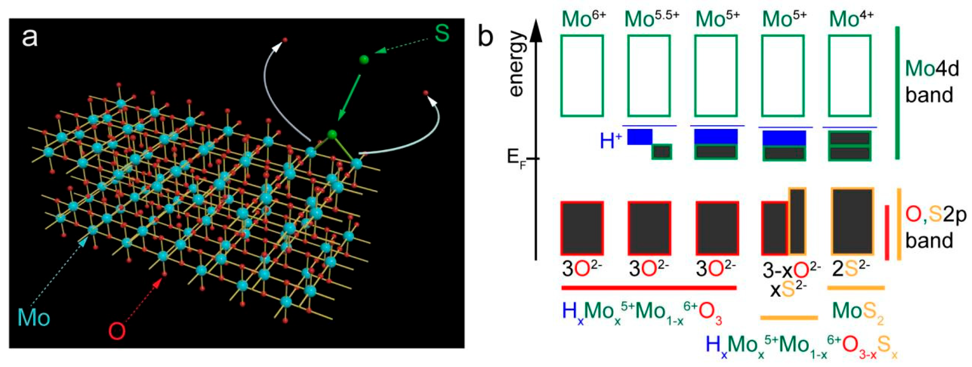
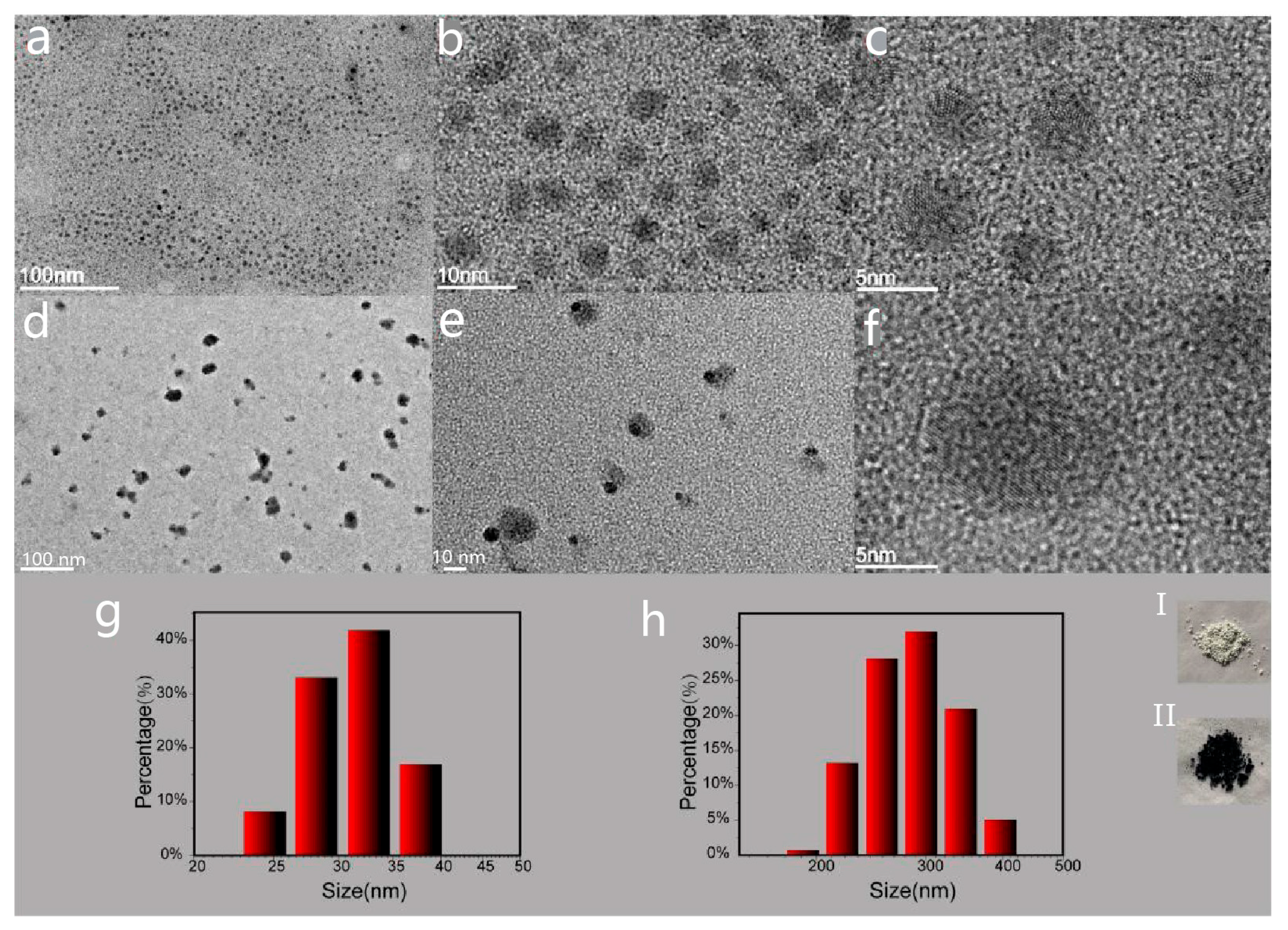
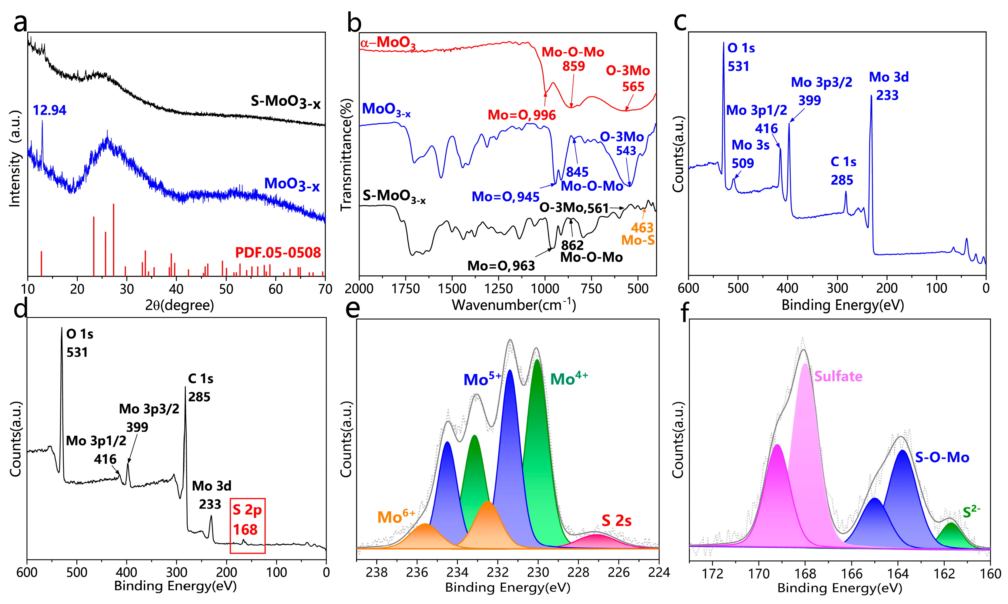
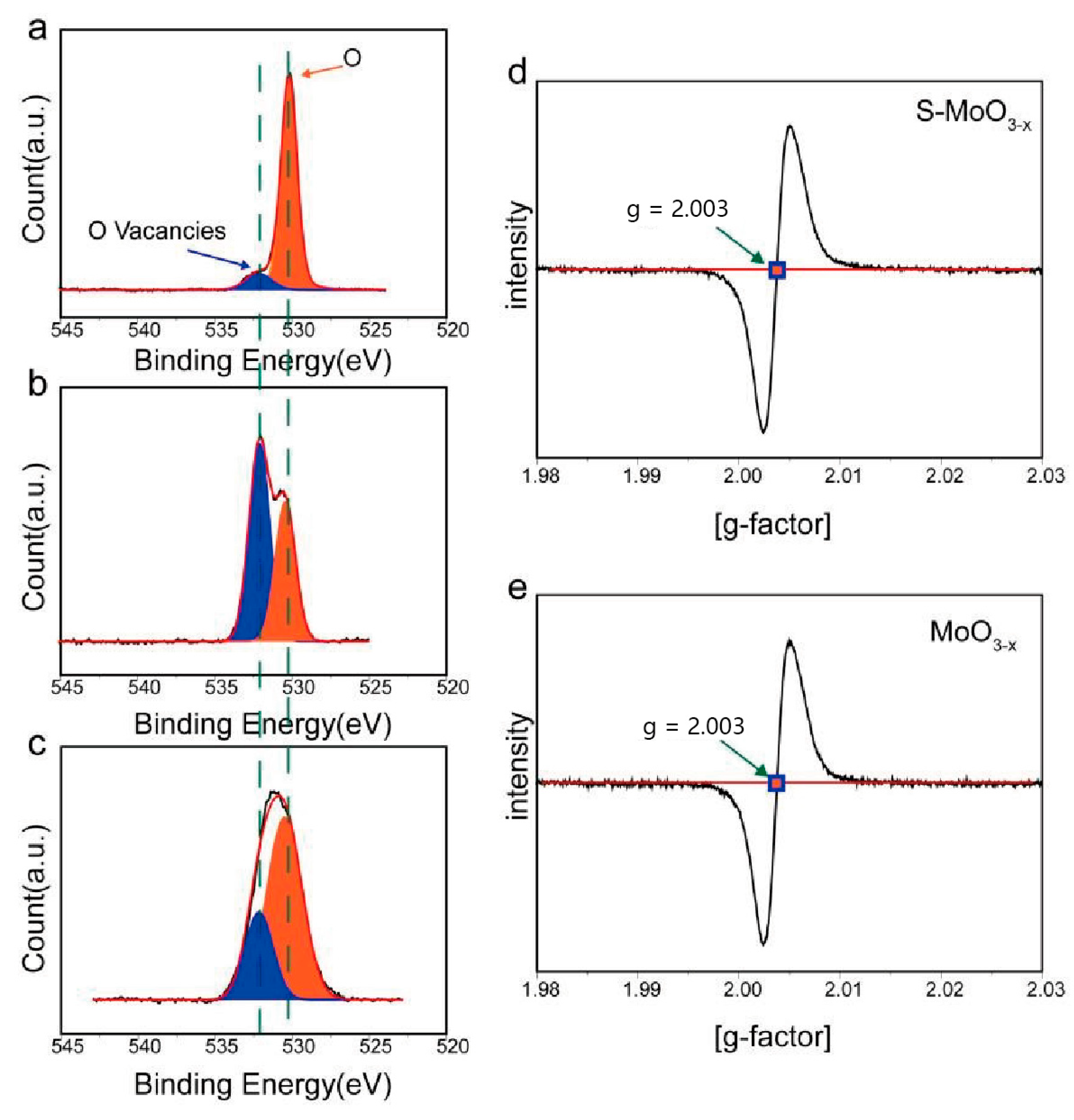
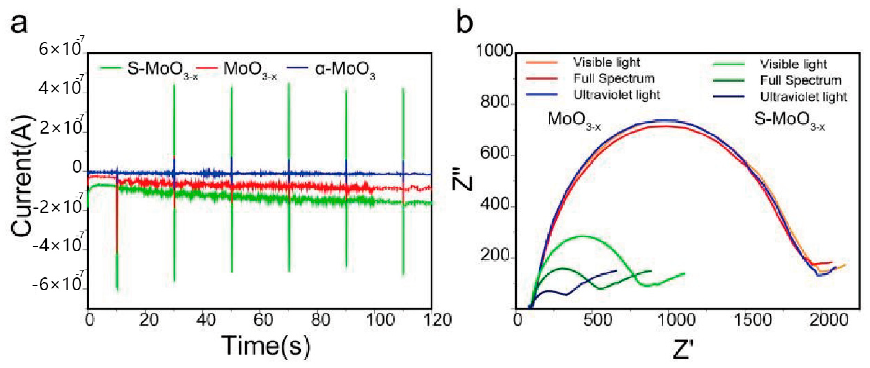
3. Results and Discussion

Typically, MoO3 exists in the form of a layered structure, where Mo atoms are surrounded by six O atoms forming octahedral structural units [22]. However, in S-MoO3−x, the structure of the material underwent changes due to the substitution of S atoms. This substitution led to the formation of Mo–S bonds (as depicted in Figure 1a), which resulted in the transition of oxide to a sulfide state. The emergence of Mo–S bonds implies the replacement of O atom positions with S atoms, which exhibit different electronic and chemical features. Meanwhile, the Mo–O bonds in MoO3 are primarily ionic, and the bonds between Mo and S display more metallic sulfide characteristics [22,23]. This transition not only induces significant changes in the chemical properties but also triggers adjustments in various aspects such as the electrical and optical properties, as elaborated subsequently.
Figure 1b depicts the process of hydrogen intercalation (essentially the appearance of O vacancies) and S doping-induced changes in the electronic band structure of MoO3. This illustrates a gradual transition from MoO3 to MoS2. In the undoped MoO3, as depicted on the far left, Mo exists in its highest oxidation state (Mo6+), corresponding to a fully occupied oxygen 2p band, which displays typical wide bandgap insulator characteristics. In this scenario, due to the lack of free charge carriers in the conduction band, the material exhibited low electrical conductivity. In the case of the hydrogen intercalation bandgap states (HxMox5+Mo1−x6+O3), when hydrogen atoms were inserted into the material, some Mo6+ ions were reduced to Mo5+ with the appearance of O vacancies, as reflected by the changes in the partially filled Mo 4d band (see Figure 1b). Electron filling resulted in a reduced bandgap and increased conductivity of the material, a key feature in electrochemical storage and chemical sensors [17,24]. In the case of the intermediate state of S doping (HxMox5+Mo1−x6+O3−xSx), with the introduction of S, the original MoO3 structure was partially replaced by S, resulting in a composite material containing a small amount of the MoS2 phase. During this process, the oxygen 2p band is affected, as it is partially replaced by the sulfur 2p band, leading to adjustments in the band structure which may influence the optical and electrical properties of the material [25,26]. In the case of the MoS2 state, on the far right of this series, complete S doping resulted in the formation of MoS2. In MoS2, the oxidation state of Mo further reduced to Mo4+, with each Mo atom coordinated with two S atoms (S2−), forming a semiconductor with a smaller bandgap. Due to there being more electrons in the conduction band, this structural change significantly enhanced the conductivity of the material. In summary, Figure 1b demonstrates how hydrogen intercalation and S doping regulate the valence states and electronic band structure of MoO3, enabling precise control over its electronic, optical, and chemical properties. Such control is crucial for developing new functional materials and optimizing the performance of existing materials.
The TEM images of MoO3−x are shown in Figure 2a–c, and the TEM images of S-MoO3−x are provided in Figure 2d–f. It can be observed that MoO3−x exhibited a more uniform dispersion, while S-MoO3−x tended to aggregate more easily. The average size of the MoO3−x particles was roughly a few nanometers, whereas for S-MoO3−x, it was approximately tens of nanometers, and lattice fringes can be seen in the high-resolution TEM images of both materials (Figure 2c,f). However, the DLS spectra (Figure 2g,h) show that the average size of MoO3−x was approximately 30 nanometers, while that of S-MoO3−x was about 300 nanometers, contradicting the TEM results. Nevertheless, the increase in statistical size can be attributed to the aggregation of small particles, which also serves as evidence for the easier aggregation of S-MoO3−x. The color change of the α-MoO3 powder from gray-white to blue-black, corresponding to the S-MoO3−x powder, is the most direct evidence of the change in the band structure of the material.
The crystalline phase of the MoO3−x nanostructures is depicted in Figure 3a. In the range from 20° to 40°, the broadening of sharp diffraction peaks can be attributed to a large number of severe lattice defects caused by oxygen vacancies. The sharp diffraction peak at 12.94° can be attributed to the α-MoO3 (020) crystal plane (JCPDF No. 05-0508) [27], suggesting that MoO3−x nanostructures preferentially form along the [0k0] direction. To further investigate the structural characteristics of S-MoO3−x, we also obtained the crystalline phase of S-MoO3−x through XRD analysis. By comparing this with the crystalline phase of the MoO3−x nanostructures, it is evident that S-MoO3−x also exhibited an amorphous structure. The disappearance of the diffraction peak at 12.94° indicates the absence of the (020) crystal plane in S-MoO3−x, which could be attributed to the introduction of more O vacancy defects during S doping. The FTIR spectra in the range of 400–2000 cm−1 (Figure 3b) confirms the successful doping of S in the S-MoO3−x (i.e., the formation of Mo-S bonds). In the α-MoO3 sample, three peaks were observed; the peak at 996 cm−1 corresponds to the stretching vibration of terminal Mo=O, indicating its orthorhombic layered MoO3 structure, the peak at 859 cm−1 represents the symmetric vibration of Mo–O−Mo bonds, and the peak at 565 cm−1 was due to the bending vibration of O atoms bonded to three metal atoms (O-3Mo) [28,29]. Both the MoO3−x and S-MoO3−x samples exhibited peaks at 945, 845, and 543 cm−1 as well as 963, 862, and 561 cm−1, attributed to the vibration modes of the Mo=O, Mo–O−Mo, and O−3Mo bonds, respectively [11,30]. In the S-MoO3−x sample, the peak at 463 cm−1 represents the vibration modes of the Mo−S bonds [31,32], providing evidence of the formation of the MoS2 phase as facilitated by the S atoms through O vacancies.
XPS analysis was conducted to further investigate the chemical composition and elemental chemical states of the samples. The XPS survey spectra of MoO3−x (Figure 3c) and S-MoO3−x (Figure 3d) revealed that the main difference between both samples was the appearance of spin-orbit splitting peaks for S2p at approximately 168 eV in the S-MoO3−x sample, evidencing the successful doping of sulfur. Figure 3e shows the high-resolution XPS spectrum of the Mo 3d region, which revealed two orbital splitting peaks at a lower binding energy (i.e., 3d5/2) and a higher binding energy (i.e., 3d3/2). The peaks at binding energies (BEs) of 230 (Mo3d5/24+) and 233.1 eV (Mo3d3/24+) can be attributed to the Mo−S bond [33]. The peaks at BEs of 231.4 (Mo3d5/25+) and 234.5 eV (Mo3d5/25+) can be attributed to MoO3−x. The peaks at BEs of 232.5 (Mo3d5/26+) and 235.6 eV (Mo3d5/26+) are ascribed to MoO3 [34]. In addition, a weak S 2s peak was detected at 227 eV, confirming the existence of MoS2 [33,34]. Furthermore, the S 2p core-level XPS spectrum of the S-MoO3−x sample is revealed in Figure 3f. A broad peak was deconvoluted into four peaks centered at 161.6, 162.8, 163.7, and 164.9 eV, corresponding to the S 2p3/2 (S2−), S 2p1/2 (S2−), S 2p3/2 (S–O–Mo), and S 2p1/2 (S–O–Mo) levels, respectively. This further indicates the existence of terminal S2− (corresponding to Mo–S) and S–O–Mo bonding in S-MoO3−x [35]. The peaks at 168 and 169.2 eV belong to the sulfate [36]. To further investigate the existence of sulfate bonds in S-MoO3−x, we performed high-resolution XPS spectroscopy analysis of the O 1s region of the α-MoO3, MoO3−x, and S-MoO3−x samples. As shown in Figure 4a–c, for all three samples, two peaks centered at 530.2 and 532.3 eV were observed, which correspond to the lattice oxygen and O vacancies in MoO3, respectively [37,38]. Among them, α-MoO3 exhibited the lowest content of O vacancies, while S-MoO3−x showed the highest one. EPR analysis of the MoO3−x and S-MoO3−x samples was further conducted, and the results are depicted in Figure 4d,e. Peaks with a g value of 2.003 were observed in both the S-MoO3−x and MoO3−x samples, which further provide evidence of the existence of O vacancies in both samples [39,40]. The analyses of XPS and EPR indicate that only lattice oxygen and O vacancies existed in S-MoO3−x, and there was no formation of SO32 or SO42 involving O or S. Therefore, the sulfate bond was attributed to the S–O bonding between the S atoms at the edge of MoS2 formed by the interaction of doped S and the O atoms of MoO3. This S–O bond suggests a covalent interaction between MoO3−x and MoS2. Such covalent bonds indicate a close contact between MoO3 and MoS2, which facilitates the transfer of electrons [41,42].
To investigate the influence of S doping on the optoelectronic properties of oxygen-deficient molybdenum oxide semiconductor materials, the S-MoO3−x and MoO3−x samples were prepared and subjected to diffuse reflectance spectroscopy (DRS), photoluminescence (PL) spectroscopy, and Mott–Schottky analysis. As shown in Figure 5a, MoO3−x exhibited a cutoff absorption edge at approximately 430 nm, while the S-MoO3−x sample demonstrated a redshift in the absorption edge compared with MoO3−x, indicating enhanced light-harvesting properties attributed to S doping. This leads to the formation of the MoS2 phase, which extends the light absorption capability of the material [43]. The corresponding main band structures of the MoO3−x and S-MoO3−x samples (Figure 5b) in the visible light region were calculated with the transformed Kubelka–Munk function (i.e., αhv = A(hv − Eg)n/2), where α is the absorption coefficient, hv is the photon energy, n is related to the type of semiconductor (the value of n is taken to be one for direct bandgap semiconductors and four for indirect bandgap semiconductors), Eg is the band gap, and A is a constant. Since MoO3 is essentially an indirect bandgap semiconductor, its n value was taken to be four [44]. In Figure 5b, it can be observed that the bandgaps of MoO3−x and S-MoO3−x were measured to be 2.68 and 2.57 eV, respectively, both of which were smaller than that of the bare α-MoO3 (Eg = 3 eV) [22]. To investigate the separation of the photo-generated electron-hole pairs in S-MoO3−x, PL analysis was performed. Figure 5c illustrates the PL spectra of MoO3−x and S-MoO3−x, both of which exhibited peaks centered at 403 nm. Interestingly, the emission peak intensity of S-MoO3−x was weaker than that of MoO3−x, confirming the rapid charge transfer between MoO3 and sulfide. This indicates a high separation efficiency of photo-generated electron-hole pairs in S-MoO3−x, resulting in effective suppression of carrier recombination [45,46] and being consistent with the XPS results. As depicted in Figure 6a, the Mott–Schottky plot reveals a significant influence of O vacancies and S doping on the flat band potential (EFB) of MoO3. The Mott–Schottky curves of α-MoO3, MoO3−x, and S-MoO3−x all exhibit positive slopes, which indicates the typical n-type semiconductor behavior. With the appearance of O vacancies and successful doping of S, EFB underwent a negative shift, suggesting an enhanced ease in the charge transfer process [47,48].
The EFB were estimated to be −0.47, −0.51, and −0.61 V versus the Ag/AgCl for α-MoO3, MoO3−x, and S-MoO3−x, respectively. The conduction band potentials (ECBs) of the n-type semiconductors were approximately 0.1 or 0.2 V lower than their flat band potentials [49]. Thus, the ECBs for MoO3−x and S-MoO3−x were estimated to be about −0.71 and −0.81 V versus the Ag/AgCl, corresponding to −0.51 and −0.61 V versus the normal hydrogen electrode (NHE) (ENHE = EAg/AgCl + 0.197 V), respectively [50]. Combined with the bandgap values obtained through UV-VIS DRS analysis (Figure 5b), the valence band potentials (EVBs) of MoO3−x and S-MoO3−x were calculated using the equation EVB = ECB + Eg [51]. More clearly, the ECB and EVB positions of MoO3−x and S-MoO3−x are summarized in Table 1.
The transient photocurrent results, illustrated in Figure 7a, indicate that S-MoO3−x exhibited a sensitive photocurrent response under visible light intermittent irradiation over several switching cycles. Among these three samples, S-MoO3−x demonstrated the highest photocurrent intensity under visible light irradiation, reflecting its superior ultraviolet light response and more effective charge separation upon light excitation [52,53]. This is consistent with the PL results (Figure 5c). Additionally, with the increase in switching cycles, the photocurrent intensity of the S-MoO3−x sample showed no significant attenuation, implying no electron-hole recombination during cycling and confirming good cycling stability [50]. In contrast, the photocurrent intensity of the MoO3−x sample gradually decreased with the increase in switching cycles, possibly due to the formation of defects (O vacancies) induced by light irradiation [54,55]. Furthermore, EIS Nyquist plots were also employed to investigate the advantage of S-MoO3−x over MoO3−x in the process of photo-generated electron-hole pair transfer. As shown in Figure 7b, we observed smaller semicircles for S-MoO3−x compared with MoO3−x under visible light, full spectrum, and ultraviolet light irradiation. This further demonstrates the effective charge separation and faster charge transfer in S-MoO3−x compared with MoO3−x [56,57]. Under visible light, full spectrum, and ultraviolet light irradiation, S-MoO3−x exhibited semicircles with different diameters, indicating that S-MoO3−x shows different charge transfer resistances (Rct) under different conditions. The largest semicircle diameter was observed under visible light irradiation, with a fitted Rct of 771 Ω. The semicircle diameter was intermediate under full spectrum light irradiation, with a fitted Rct of 511 Ω. The smallest semicircle was observed under ultraviolet light irradiation, with an Rct of 296 Ω. These results demonstrate that S-MoO3−x had the lowest charge transfer resistance under ultraviolet light irradiation [58]. The charge transfer resistance of MoO3−x showed almost no change in these three cases, and after fitting, Rct = 1941 Ω. The current–voltage curve (Figure 8) also shows that the resistance of MoO3−x was much greater than that of S-MoO3−x. However, the photo-response values of both materials exhibited the same phenomenon; the current was highest under UV light followed by visible light, and it was lowest in darkness. For S-MoO3−x, both the reduction in resistance under light exposure and the generation of photocurrent contributed to the increase in current. In contrast, for MoO3−x, we believe that the increase in current was solely due to the generation of photocurrent. This result is also consistent with the analysis in Figure 7.

4. Conclusions

In summary, we successfully fabricated S-MoO3−x nanostructures via the hydrothermal process and systematically investigated the effect of S doping on the morphology and optoelectronic properties of MoO3. The introduction of S atoms substituted some oxygen atoms and generated MoS2 with the S atoms bonded to oxygen atoms in the MoO3, resulting in S–O bonds. The MoS2 phase formed by S doping exhibited dual functionality, acting as a sensitizing unit to induce visible light response and enhancing the rate of the charge carrier’s separation. Therefore, due to the enhanced visible light absorption and rapid charge carrier’s separation, S-MoO3−x holds promise as a potential photocatalytic material. This work presents a simple and efficient strategy for modifying MoO3 with S doping which significantly improves the optoelectronic performance of MoO3 compared with the sole oxygen vacancies introduced into MoO3.

5. Patents

This work is related to Chinese Patent Application Number 2022110784700.

Author Contributions

Formal analysis, M.H. and Y.A.A. investigation, J.Y.; writing—original draft preparation, Z.Z.; writing—review and editing, A.W. All authors have read and agreed to the published version of the manuscript.

Funding

This research was funded by the Natural Science Foundation of Top Talent of SZTU (grant no. GDRC202139) and National Natural Science Foundation of China (12104323).

Data Availability Statement

Dataset available on request from the authors.

Acknowledgments

M. Humayun would like to acknowledge Prince Sultan University.

Conflicts of Interest

The authors declare no conflicts of interest.

References

  1. Peng, J.; Shen, J.; Yu, X.; Tang, H.; Zulfiqar; Liu, Q. Construction of LSPR-Enhanced 0D/2D CdS/MoO3−x S-Scheme Heterojunctions for Visible-Light-Driven Photocatalytic H2 Evolution. Chin. J. Catal. 2021, 42, 87–96. [Google Scholar] [CrossRef]
  2. Zhang, Y.; Chen, P.; Wang, Q.; Wang, Q.; Zhu, K.; Ye, K.; Wang, G.; Cao, D.; Yan, J.; Zhang, Q. High-Capacity and Kinetically Accelerated Lithium Storage in MoO3 Enabled by Oxygen Vacancies and Heterostructure. Adv. Energy Mater. 2021, 11, 2101712. [Google Scholar] [CrossRef]
  3. Hou, F.; Su, Z.; Jin, F.; Yan, X.; Wang, L.; Zhao, H.; Zhu, J.; Chu, B.; Li, W. Efficient and Stable Planar Heterojunction Perovskite Solar Cells with an MoO3/PEDOT:PSS Hole Transporting Layer. Nanoscale 2015, 7, 9427–9432. [Google Scholar] [CrossRef] [PubMed]
  4. Yang, J.; Xiao, X.; Chen, P.; Zhu, K.; Cheng, K.; Ye, K.; Wang, G.; Cao, D.; Yan, J. Creating Oxygen-Vacancies in MoO3−x Nanobelts toward High Volumetric Energy-Density Asymmetric Supercapacitors with Long Lifespan. Nano Energy 2019, 58, 455–465. [Google Scholar] [CrossRef]
  5. Prasomsri, T.; Shetty, M.; Murugappan, K.; Román-Leshkov, Y. Insights into the Catalytic Activity and Surface Modification of MoO3 during the Hydrodeoxygenation of Lignin-Derived Model Compounds into Aromatic Hydrocarbons under Low Hydrogen Pressures. Energy Environ. Sci. 2014, 7, 2660–2669. [Google Scholar] [CrossRef]
  6. Xu, Y.; Wang, X.; Zhang, W.L.; Lv, F.; Guo, S. Recent Progress in Two-Dimensional Inorganic Quantum Dots. Chem. Soc. Rev. 2018, 47, 586–625. [Google Scholar] [CrossRef] [PubMed]
  7. Yang, Y.; Lau, K.Y.; Zheng, J.; Dong, J.; Wang, L.; Wang, W.; Xu, B.; Qiu, J.; Liu, X. Coupled Femtosecond Laser Assisted Doping and Fragmentation of MoO3 Nanosheets Generates Plasmonic QDs with Strong NLO Response. Adv. Opt. Mater. 2023, 11, 2202900. [Google Scholar] [CrossRef]
  8. Li, Y.; Mi, Y.; Liu, Z.; Liu, Y.; Zhang, W.; Qiu, S.; Ramos, M.A.; Hu, T.S.; Xu, Q. MoO3−x Quantum Dots-Based Hydrogel with Excellent Light-Triggered Self-Healing Efficiency and Pressure Sensitive Photoluminescence for Accurate Remote Force Measurement. Mater. Today Phys. 2022, 27, 100807. [Google Scholar] [CrossRef]
  9. Zheng, B.; Fan, J.; Chen, B.; Qin, X.; Wang, J.; Wang, F.; Deng, R.; Liu, X. Rare-Earth Doping in Nanostructured Inorganic Materials. Chem. Rev. 2022, 122, 5519–5603. [Google Scholar] [CrossRef]
  10. Wang, J.; Zhou, Q.; Wei, Z.; Xu, L.; Zeng, W. Experimental and Theoretical Studies of Zn-Doped MoO3 Hierarchical Microflower with Excellent Sensing Performances to Carbon Monoxide. Ceram. Int. 2020, 46 Pt A, 29222–29232. [Google Scholar] [CrossRef]
  11. Mohamed, M.M.; Salama, T.M.; Morsy, M.; Shahba, R.M.A.; Mohamed, S.H. Facile Strategy of Synthesizing α-MoO3−x Nanorods Boosted as Traced by 1% Graphene Oxide: Efficient Visible Light Photocatalysis and Gas Sensing Applications. Sens. Actuators B Chem. 2019, 299, 126960. [Google Scholar] [CrossRef]
  12. Xu, L.; Zhou, W.; Chao, S.; Liang, Y.; Zhao, X.; Liu, C.; Xu, J. Advanced Oxygen-Vacancy Ce-Doped MoO3 Ultrathin Nanoflakes Anode Materials Used as Asymmetric Supercapacitors with Ultrahigh Energy Density. Adv. Energy Mater. 2022, 12, 2200101. [Google Scholar] [CrossRef]
  13. Chen, K.; Wang, J.; Zhang, H.; Ma, D.; Chu, K. Self-Tandem Electrocatalytic NO Reduction to NH3 on a W Single-Atom Catalyst. Nano Lett. 2023, 23, 1735–1742. [Google Scholar] [CrossRef]
  14. Ijeh, R.O.; Nwanya, A.C.; Nkele, A.C.; Madiba, I.G.; Bashir, A.K.H.; Ekwealor, A.B.C.; Osuji, R.U.; Maaza, M.; Ezema, F. Optical, Electrical and Magnetic Properties of Copper Doped Electrodeposited MoO3 Thin Films. Ceram. Int. 2020, 46 Pt A, 10820–10828. [Google Scholar] [CrossRef]
  15. Zheng, C.; Luo, N.; Huang, S.; Wu, W.; Huang, H.; Wei, M. Nanocomposite of Mo2N Quantum Dots@MoO3@Nitrogen-Doped Carbon as a High-Performance Anode for Lithium-Ion Batteries. ACS Sustain. Chem. Eng. 2019, 7, 10198–10206. [Google Scholar] [CrossRef]
  16. Gao, P.; Ru, Q.; Pan, Z.; Zhang, J.; Xu, W.; Chi-Chung Ling, F.; Wei, L. Robust Hetero-MoO3/MoO2@N-Doped Carbon Nanobelts Decorated with Oxygen Deficiencies as High-Performance Anodes for Potassium/Sodium Storage. J. Colloid Interface Sci. 2021, 599, 730–740. [Google Scholar] [CrossRef] [PubMed]
  17. Kim, H.-S.; Cook, J.B.; Lin, H.; Ko, J.S.; Tolbert, S.H.; Ozolins, V.; Dunn, B. Oxygen Vacancies Enhance Pseudocapacitive Charge Storage Properties of MoO3−x. Nat. Mater. 2017, 16, 454–460. [Google Scholar] [CrossRef]
  18. Luo, Z.; Miao, R.; Huan, T.D.; Mosa, I.M.; Poyraz, A.S.; Zhong, W.; Cloud, J.E.; Kriz, D.A.; Thanneeru, S.; He, J.; et al. Mesoporous MoO3−x Material as an Efficient Electrocatalyst for Hydrogen Evolution Reactions. Adv. Energy Mater. 2016, 6, 1600528. [Google Scholar] [CrossRef]
  19. Yu, M.; Cheng, X.; Zeng, Y.; Wang, Z.; Tong, Y.; Lu, X.; Yang, S. Dual-Doped Molybdenum Trioxide Nanowires: A Bifunctional Anode for Fiber-Shaped Asymmetric Supercapacitors and Microbial Fuel Cells. Angew. Chem. Int. Ed. 2016, 55, 6762–6766. [Google Scholar] [CrossRef]
  20. Yu, X.; Qiu, P.; Wang, Y.; He, B.; Xu, X.; Zhu, H.; Ding, J.; Liu, X.; Li, Z.; Wang, Y. Defect-Induced Charge Redistribution of MoO3−x Nanometric Wires for Photocatalytic Ammonia Synthesis. J. Colloid Interface Sci. 2023, 640, 775–782. [Google Scholar] [CrossRef]
  21. Teng, Y.; Zhou, Q.; Gao, P. Applications and Challenges of Elemental Sulfur, Nanosulfur, Polymeric Sulfur, Sulfur Composites, and Plasmonic Nanostructures. Crit. Rev. Environ. Sci. Technol. 2019, 49, 2314–2358. [Google Scholar] [CrossRef]
  22. De Castro, I.A.; Datta, R.S.; Ou, J.Z.; Castellanos-Gomez, A.; Sriram, S.; Daeneke, T.; Kalantar-Zadeh, K. Molybdenum Oxides—From Fundamentals to Functionality. Adv. Mater. 2017, 29, 1701619. [Google Scholar] [CrossRef] [PubMed]
  23. Ganatra, R.; Zhang, Q. Few-Layer MoS2: A Promising Layered Semiconductor. ACS Nano 2014, 8, 4074–4099. [Google Scholar] [CrossRef] [PubMed]
  24. Ahmadzadeh, Z.; Ranjbar, M. Plasmonic MoO3−x Nanosheets by Anodic Oxidation of Molybdenum for Colorimetric Sensing of Hydrogen Peroxide. Anal. Chim. Acta 2022, 1198, 339529. [Google Scholar] [CrossRef] [PubMed]
  25. Guo, S.; Li, X.; Ren, X.; Yang, L.; Zhu, J.; Wei, B. Optical and Electrical Enhancement of Hydrogen Evolution by MoS2@MoO3 Core–Shell Nanowires with Designed Tunable Plasmon Resonance. Adv. Funct. Mater. 2018, 28, 1802567. [Google Scholar] [CrossRef]
  26. Kim, M.; Kwon, B.-H.; Joo, C.W.; Cho, M.S.; Jang, H.; Kim, Y.; Cho, H.; Jeon, D.Y.; Cho, E.N.; Jung, Y.S. Metal Oxide Charge Transfer Complex for Effective Energy Band Tailoring in Multilayer Optoelectronics. Nat. Commun. 2022, 13, 75. [Google Scholar] [CrossRef] [PubMed]
  27. Hu, B.; Mai, L.; Chen, W.; Yang, F. From MoO3 Nanobelts to MoO2 Nanorods: Structure Transformation and Electrical Transport. ACS Nano 2009, 3, 478–482. [Google Scholar] [CrossRef] [PubMed]
  28. Sen, S.K.; Dutta, S.; Khan, M.R.; Manir, M.S.; Dutta, S.; Al Mortuza, A.; Razia, S.; Hakim, M.A. Characterization and Antibacterial Activity Study of Hydrothermally Synthesized H-MoO3 Nanorods and α-MoO3 Nanoplates. BioNanoScience 2019, 9, 873–882. [Google Scholar] [CrossRef]
  29. Maheswari, N.; Muralidharan, G. Controlled Synthesis of Nanostructured Molybdenum Oxide Electrodes for High Performance Supercapacitor Devices. Appl. Surf. Sci. 2017, 416, 461–469. [Google Scholar] [CrossRef]
  30. Lima, C.D.A.; Barbosa Moura, J.V.; de Castro Maciel, A.; Luz-Lima, C.; Sinimbu, L.I.M.; Chaves, J.F.; Oliveira, J.D.S.; Syed, A.R.; Sommer, R.L.; Ghosh, A.; et al. Synthesis and Magnetic Characterization of Iron-Doped Molybdenum Trioxide (α-MoO3:xFe). Solid State Sci. 2023, 145, 107313. [Google Scholar] [CrossRef]
  31. Liu, S.; Zhang, X.; Shao, H.; Xu, J.; Chen, F.; Feng, Y. Preparation of MoS2 Nanofibers by Electrospinning. Mater. Lett. 2012, 73, 223–225. [Google Scholar] [CrossRef]
  32. Saleem, S.; Salman, M.; Ali, S.; Ling, Y.; Khan, M. Electrocatalytic Hydrogen Evolution Reaction on Sulfur-Deficient MoS2 Nanostructures. Int. J. Hydrogen Energy 2022, 47, 7713–7723. [Google Scholar] [CrossRef]
  33. Kondekar, N.P.; Boebinger, M.G.; Woods, E.V.; McDowell, M.T. In Situ XPS Investigation of Transformations at Crystallographically Oriented MoS2 Interfaces. ACS Appl. Mater. Interfaces 2017, 9, 32394–32404. [Google Scholar] [CrossRef] [PubMed]
  34. Wang, B.; Ang, E.H.; Yang, Y.; Zhang, Y.; Geng, H.; Ye, M.; Li, C.C. Interlayer Engineering of Molybdenum Trioxide toward High-Capacity and Stable Sodium Ion Half/Full Batteries. Adv. Funct. Mater. 2020, 30, 2001708. [Google Scholar] [CrossRef]
  35. Liu, S.; Xu, C.; Yang, H.; Qian, G.; Hua, S.; Liu, J.; Zheng, X.; Lu, X. Atomic Modulation Triggering Improved Performance of MoO3 Nanobelts for Fiber-Shaped Supercapacitors. Small 2020, 16, 1905778. [Google Scholar] [CrossRef] [PubMed]
  36. Liu, D.; Jin, Z.; Bi, Y. Charge Transmission Channel Construction between a MOF and rGO by Means of Co–Mo–S Modification. Catal. Sci. Technol. 2017, 7, 4478–4488. [Google Scholar] [CrossRef]
  37. Huang, Z.; Liu, J.; Zong, S.; Wang, X.; Chen, K.; Liu, L.; Fang, Y. Fabrication of Graphitic Carbon Nitride/Nonstoichiometric Molybdenum Oxide Nanorod Composite with the Nonmetal Plasma Enhanced Photocatalytic Hydrogen Evolution Activity. J. Colloid Interface Sci. 2022, 606, 848–859. [Google Scholar] [CrossRef]
  38. Bharathi, M.; Balraj, B.; Sivakumar, C.; Wang, Z.; Shuai, J.; Ho, M.-S.; Guo, D. Effect of Ag Doping on Bipolar Switching Operation in Molybdenum Trioxide (MoO3) Nanostructures for Non-Volatile Memory. J. Alloys Compd. 2021, 862, 158035. [Google Scholar] [CrossRef]
  39. Liu, Q.; Wu, Y.; Zhang, J.; Chen, K.; Huang, C.; Chen, H.; Qiu, X. Plasmonic MoO3−x Nanosheets with Tunable Oxygen Vacancies as Efficient Visible Light Responsive Photocatalyst. Appl. Surf. Sci. 2019, 490, 395–402. [Google Scholar] [CrossRef]
  40. Zhang, Y.; Ping, X.; Hao, L.; He, Y.; Guo, Y.; Zhao, Q.; Zheng, Z.; Lu, Y. Facile Preparation of Anodized MoO3−x Films and Their Boosted Photocatalytic Activity. J. Environ. Chem. Eng. 2021, 9, 105565. [Google Scholar] [CrossRef]
  41. Sari, F.N.I.; Ting, J.-M. MoS2/MoOx-Nanostructure-Decorated Activated Carbon Cloth for Enhanced Supercapacitor Performance. ChemSusChem 2018, 11, 897–906. [Google Scholar] [CrossRef] [PubMed]
  42. Deng, Y.; Zhao, Y.; Peng, K.; Yu, L. One-Step Hydrothermal Synthesis of MoO2/MoS2 Nanocomposites as High-Performance Electrode Material for Supercapacitors. ACS Appl. Mater. Interfaces 2022, 14, 49909–49918. [Google Scholar] [CrossRef] [PubMed]
  43. Kite, S.V.; Kadam, A.N.; Sathe, D.J.; Patil, S.; Mali, S.S.; Hong, C.K.; Lee, S.; Garadkar, K.M. Nanostructured TiO2 Sensitized with MoS2 Nanoflowers for Enhanced Photodegradation Efficiency toward Methyl Orange. ACS Omega 2021, 6, 17071–17085. [Google Scholar] [CrossRef] [PubMed]
  44. Xie, Z.; Feng, Y.; Wang, F.; Chen, D.; Zhang, Q.; Zeng, Y.; Lv, W.; Liu, G. Construction of Carbon Dots Modified MoO3/g-C3N4 Z-Scheme Photocatalyst with Enhanced Visible-Light Photocatalytic Activity for the Degradation of Tetracycline. Appl. Catal. B Environ. 2018, 229, 96–104. [Google Scholar] [CrossRef]
  45. Wei, W.; Tian, Q.; Sun, H.; Liu, P.; Zheng, Y.; Fan, M.; Zhuang, J. Efficient Visible-Light-Driven Photocatalytic H2 Evolution over MoO2-C/CdS Ternary Heterojunction with Unique Interfacial Microstructures. Appl. Catal. B Environ. 2020, 260, 118153. [Google Scholar] [CrossRef]
  46. Yang, Y.-Y.; Feng, H.-P.; Niu, C.-G.; Huang, D.-W.; Guo, H.; Liang, C.; Liu, H.-Y.; Chen, S.; Tang, N.; Li, L. Constructing a Plasma-Based Schottky Heterojunction for near-Infrared-Driven Photothermal Synergistic Water Disinfection: Synergetic Effects and Antibacterial Mechanisms. Chem. Eng. J. 2021, 426, 131902. [Google Scholar] [CrossRef]
  47. Kurnia, F.; Ng, Y.H.; Amal, R.; Valanoor, N.; Hart, J.N. Defect Engineering of ZnS Thin Films for Photoelectrochemical Water-Splitting under Visible Light. Sol. Energy Mater. Sol. Cells 2016, 153, 179–185. [Google Scholar] [CrossRef]
  48. Hao, X.; Wang, Y.; Zhou, J.; Cui, Z.; Wang, Y.; Zou, Z. Zinc Vacancy-Promoted Photocatalytic Activity and Photostability of ZnS for Efficient Visible-Light-Driven Hydrogen Evolution. Appl. Catal. B Environ. 2018, 221, 302–311. [Google Scholar] [CrossRef]
  49. Li, X.; Yu, J.; Low, J.; Fang, Y.; Xiao, J.; Chen, X. Engineering Heterogeneous Semiconductors for Solar Water Splitting. J. Mater. Chem. A 2015, 3, 2485–2534. [Google Scholar] [CrossRef]
  50. Yi, S.-S.; Yan, J.-M.; Wulan, B.-R.; Li, S.-J.; Liu, K.-H.; Jiang, Q. Noble-Metal-Free Cobalt Phosphide Modified Carbon Nitride: An Efficient Photocatalyst for Hydrogen Generation. Appl. Catal. B Environ. 2017, 200, 477–483. [Google Scholar] [CrossRef]
  51. Yang, Y.-Y.; Niu, C.-G.; Huang, D.-W.; Guo, H.; Feng, H.-P.; Li, L.; Liu, H.-Y.; Fan, Q.-Q.; Qin, M.-Z. Appropriate Oxygen Vacancies and Mo-N Bond Synergistically Modulate Charge Transfer Dynamics of MoO3−x/S-CN for Superior Photocatalytic Disinfection: Unveiling Synergistic Effects and Disinfection Mechanism. J. Hazard. Mater. 2023, 445, 130481. [Google Scholar] [CrossRef]
  52. Jiang, T.; Wang, K.; Guo, T.; Wu, X.; Zhang, G. Fabrication of Z-Scheme MoO3/Bi2O4 Heterojunction Photocatalyst with Enhanced Photocatalytic Performance under Visible Light Irradiation. Chin. J. Catal. 2020, 41, 161–169. [Google Scholar] [CrossRef]
  53. Zhang, Y.; Park, S.-J. Facile Construction of MoO3@ZIF-8 Core-Shell Nanorods for Efficient Photoreduction of Aqueous Cr (VI). Appl. Catal. B Environ. 2019, 240, 92–101. [Google Scholar] [CrossRef]
  54. Xu, H.; Zhang, L.; Wang, A.; Hou, J.; Guo, X. Facile Preparation of Oxygen-Vacancy-Engineered MoOx Nanostructures for Photoreversible Switching Systems. Nanomaterials 2021, 11, 3192. [Google Scholar] [CrossRef] [PubMed]
  55. Yang, W.; Prabhakar, R.R.; Tan, J.; Tilley, S.D.; Moon, J. Strategies for Enhancing the Photocurrent, Photovoltage, and Stability of Photoelectrodes for Photoelectrochemical Water Splitting. Chem. Soc. Rev. 2019, 48, 4979–5015. [Google Scholar] [CrossRef] [PubMed]
  56. Xu, J.; Li, Q.; Liu, X.; Yang, Q. P-Doped Nanorod MoO3 and Nanoflower NiAl-LDH Construct S-Type Heterojunction for Photocatalytic High-Efficiency Hydrogen Evolution. Surf. Interfaces 2023, 43, 103593. [Google Scholar] [CrossRef]
  57. Liu, X.; Luo, Y.; Ling, C.; Shi, Y.; Zhan, G.; Li, H.; Gu, H.; Wei, K.; Guo, F.; Ai, Z.; et al. Rare Earth La Single Atoms Supported MoO3−x for Efficient Photocatalytic Nitrogen Fixation. Appl. Catal. B Environ. 2022, 301, 120766. [Google Scholar] [CrossRef]
  58. Ye, L.; Han, C.; Ma, Z.; Leng, Y.; Li, J.; Ji, X.; Bi, D.; Xie, H.; Huang, Z. Ni2P Loading on Cd0.5Zn0.5S Solid Solution for Exceptional Photocatalytic Nitrogen Fixation under Visible Light. Chem. Eng. J. 2017, 307, 311–318. [Google Scholar] [CrossRef]
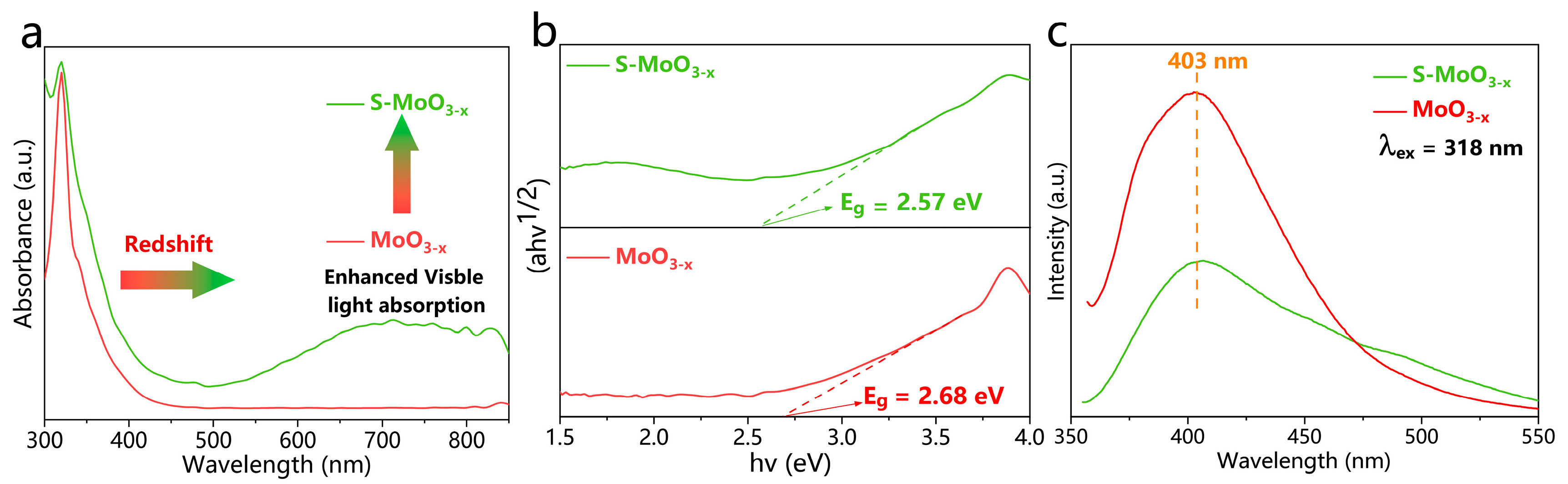
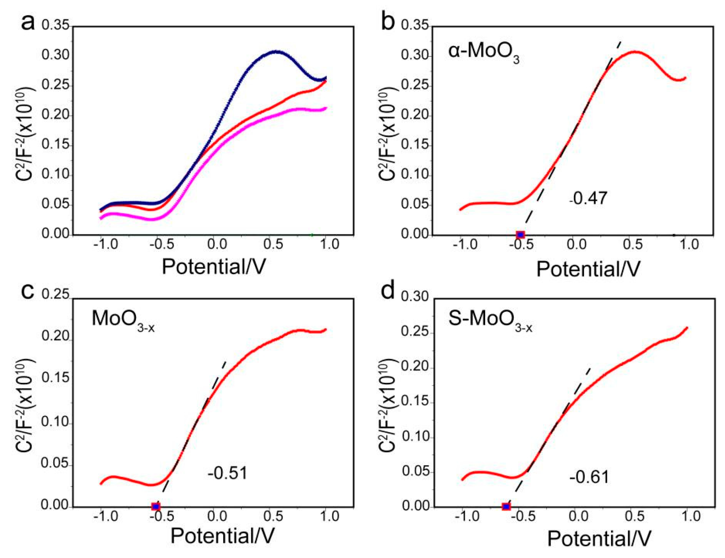
Figure 1. (a) Schematic of the S–doped MoO3−x. (b) Changes in electronic structure due to hydrogen intercalation and S doping. Bandgap states formed by hydrogen intercalation (blue) and “valence band-like Mo5+ state” (in the green box, black means occupied, and white means unoccupied), as indicated by the widths of the electronic states.
Nanomaterials 14 01189 g001
Figure 2. (ac) TEM images of MoO3−x. (df) TEM images of S-MoO3−x. (g) DLS spectrum of MoO3−x. (h) DLS spectrum of S-MoO3−x. (h, I) Physical image of α-MoO3 powder. (h, II) Physical image of S-MoO3−x powder.
Nanomaterials 14 01189 g002
Figure 3. (a) XRD spectra of MoO3−x and S-MoO3−x. (b) Fourier transform infrared spectra of α-MoO3, MoO3−x, and S-MoO3−x. (c) XPS survey spectrum of MoO3−x. (d) XPS survey spectrum of S-MoO3−x. (e) High–resolution XPS spectrum of the Mo 3d region in S-MoO3−x. (f) High-resolution XPS spectrum of the S 2p region in S-MoO3−x.
Nanomaterials 14 01189 g003
Figure 4. (a) High–resolution XPS spectrum of the O 1s region for α-MoO3. (b) High–resolution XPS spectrum of the O 1s region for S-MoO3−x. (c) High-resolution XPS spectrum of the O 1s region for MoO3−x. (d) EPR spectrum of S-MoO3−x. (e) EPR spectrum of MoO3−x.
Nanomaterials 14 01189 g004
Figure 5. (a) UV–VIS DRS spectra of S-MoO3−x and MoO3−x samples. (b) Curves of (αhν) 1/2 versus hν for S-MoO3−x and MoO3−x samples. (c) Photoluminescence spectra of MoO3−x and S-MoO3−x.
Nanomaterials 14 01189 g005
Figure 6. (a) Mott–Schottky plot of α-MoO3, MoO3−x, and S-MoO3−x at fixed frequency of 1 kHz, (b) Mott–Schottky plot of α-MoO3, (c) Mott–Schottky plot of MoO3−x, and (d) Mott–Schottky plot of S-MoO3−x.
Nanomaterials 14 01189 g006
Figure 7. (a) Transient photocurrent responses of α-MoO3, MoO3−x, and S-MoO3−x under ultraviolet light illumination. (b) Electrochemical impedance spectroscopy (EIS) Nyquist plots of MoO3−x and S-MoO3−x under visible light, full spectrum, and ultraviolet light illumination.
Nanomaterials 14 01189 g007
Figure 8. (a,b) Current–voltage curves of MoO3−x and S-MoO3−x under dark, visible light, and ultraviolet light illumination.
Nanomaterials 14 01189 g008
Table 1. Calculated ECB and EVB values for MoO3−x and S-MoO3−x.
SemiconductorEg (eV)ECB (eV)EVB (eV)
MoO3−x2.68−0.512.17
S-MoO3−x2.57−0.611.96
Disclaimer/Publisher’s Note: The statements, opinions and data contained in all publications are solely those of the individual author(s) and contributor(s) and not of MDPI and/or the editor(s). MDPI and/or the editor(s) disclaim responsibility for any injury to people or property resulting from any ideas, methods, instructions or products referred to in the content.

