
Physical Properties of CaTiO3-Modified NaNbO3 Thin Films

Abstract
1. Introduction
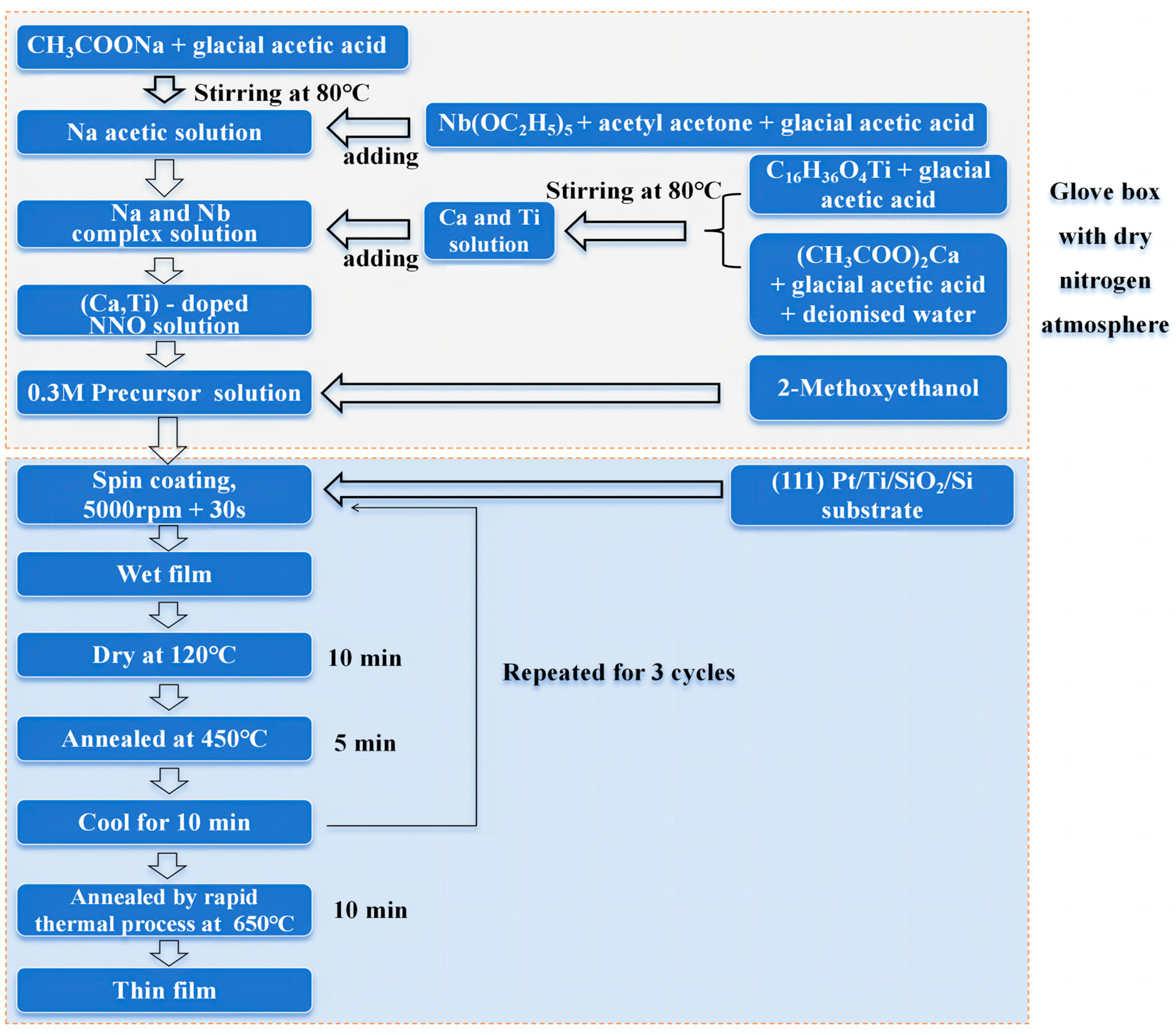
2. Experimental
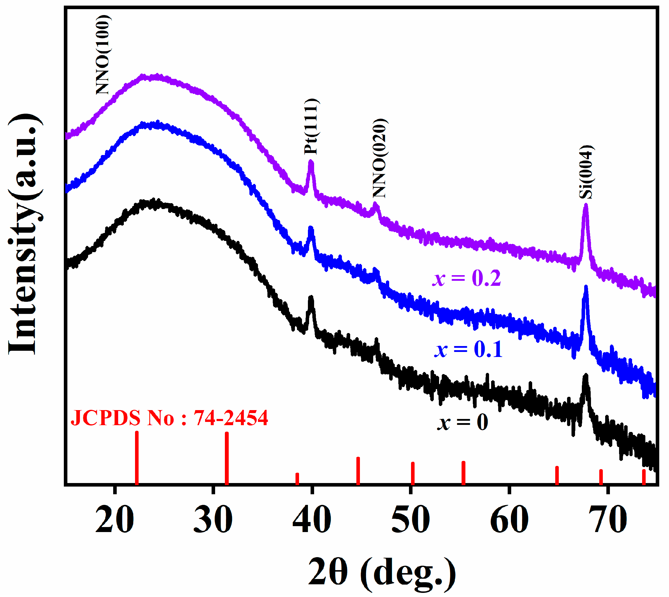
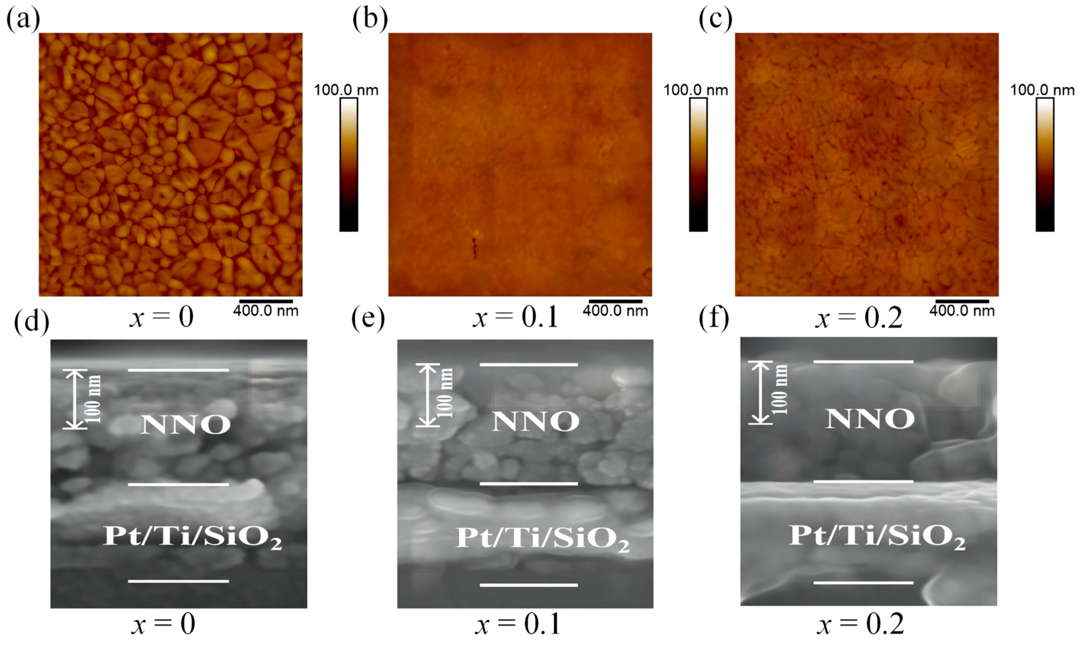
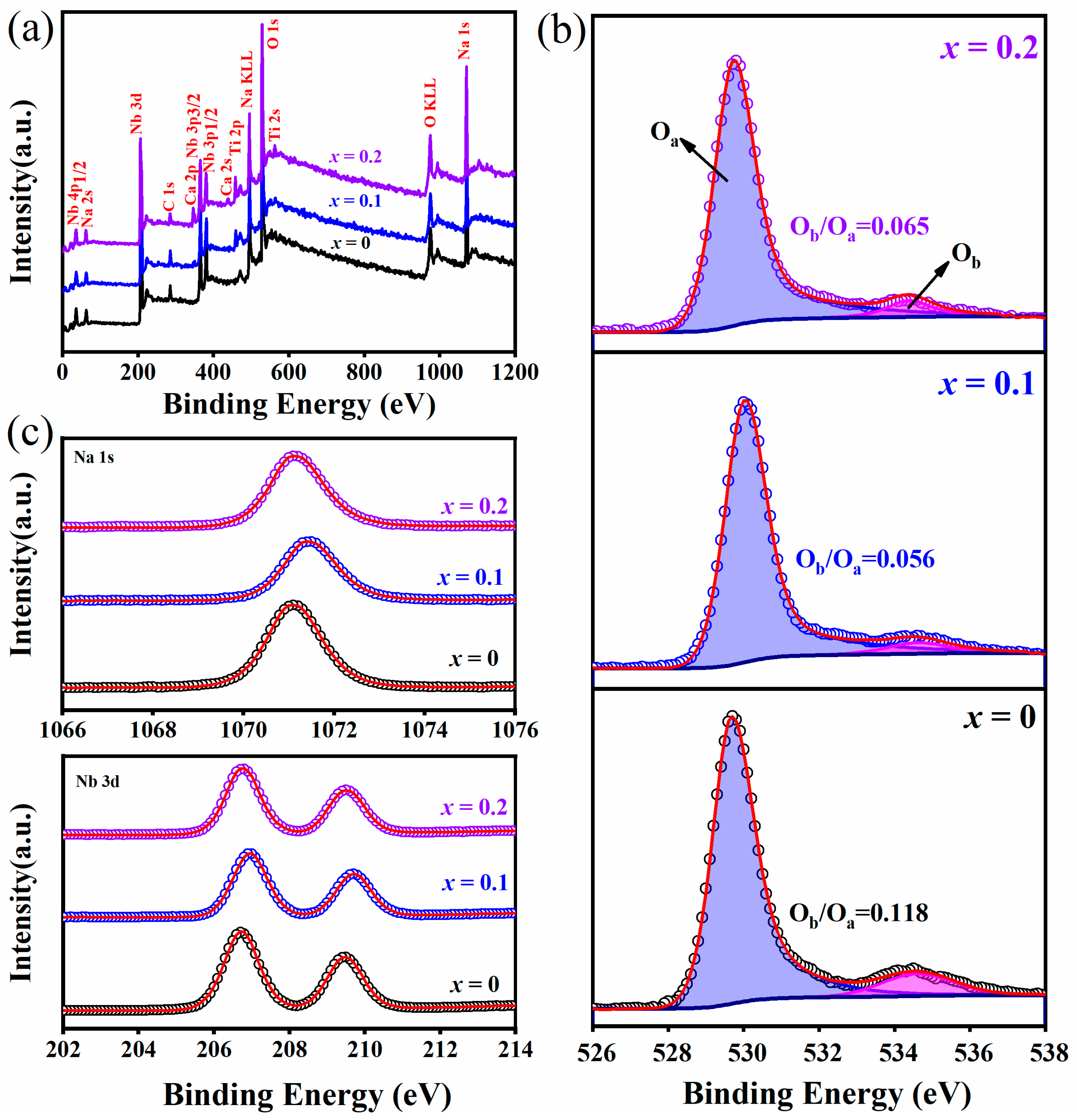
3. Results and Discussion
4. Conclusions
Author Contributions
Funding
Data Availability Statement
Conflicts of Interest
References
- Shirane, G.; Newnham, R.; Pepinsky, R. Dielectric properties and phase transitions of NaNbO3 and (Na, K)NbO3. Phys. Rev. 1954, 96, 581–588. [Google Scholar] [CrossRef]
- Saito, Y.; Takao, H.; Tani, T.; Nonoyama, T.; Takatori, K.; Homma, T.; Nagaya, T.; Nakamura, M. Lead-free piezoceramics. Nature 2004, 432, 84–87. [Google Scholar] [CrossRef]
- Mishra, S.K.; Choudhury, N.; Chaplot, S.L.; Krishna, P.S.R.; Mittal, R. Competing antiferroelectric and ferroelectric interactions in NaNbO3: Neutron diffraction and theoretical studies. Phys. Rev. B 2007, 76, 024110. [Google Scholar] [CrossRef]
- Johnston, K.E.; Tang, C.C.; Parker, J.E.; Knight, K.S.; Lightfoot, P.; Ashbrook, S.E. The polar phase of NaNbO3: A combined study by powder diffraction, solid-state NMR, and first-principles calculations. J. Am. Chem. Soc. 2010, 132, 8732–8746. [Google Scholar] [CrossRef] [PubMed]
- Yuzyuk, Y.; Shakhovoy, R.; Raevskaya, S.I.; Raevski, I.; Marssi, M.; Karkut, M.; Simon, P. Ferroelectric Q-phase in a NaNbO3 epitaxial thin film. Appl. Phys. Lett. 2010, 96, 222904. [Google Scholar] [CrossRef]
- Wu, J.G.; Xiao, D.Q.; Zhu, J.G. Potassium-sodium niobate lead-free piezoelectric materials: Past, present, and future of phase boundaries. Chem. Rev. 2015, 1157, 2559–2595. [Google Scholar] [CrossRef] [PubMed]
- Qi, H.; Zuo, R.Z.; Xie, A.W.; Tian, A.; Fu, J.; Zhang, Y.; Zhang, S.J. Ultrahigh energy-storage density in NaNbO3-based lead-free relaxor antiferroelectric ceramics with nanoscale domains. Adv. Funct. Mater 2019, 29, 1903877. [Google Scholar] [CrossRef]
- Xie, A.; Qi, H.; Zuo, R. Achieving remarkable amplification of energy-storage density in two-step sintered NaNbO3-SrTiO3 antiferroelectric capacitors through dual adjustment of local heterogeneity and grain scale. ACS Appl. Mater. Interfaces 2020, 12, 19467–19475. [Google Scholar] [CrossRef]
- Tian, A.; Zuo, R.Z.; Qi, H.; Shi, M. Large energy-storage density in transition-metal oxide modified NaNbO3-Bi(Mg0.5Ti0.5)O3 lead-free ceramics through regulating the antiferroelectric phase structure. J. Mater. Chem. A 2020, 8, 8352–8359. [Google Scholar] [CrossRef]
- Dong, X.Y.; Li, X.; Chen, X.L.; Chen, H.Y.; Sun, C.C.; Shi, J.P.; Pang, F.H.; Zhou, H.F. High energy storage density and power density achieved simultaneously in NaNbO3-based lead-free ceramics via antiferroelectricity enhancement. J. Mater. 2021, 7, 629–639. [Google Scholar] [CrossRef]
- Jiang, J.; Meng, X.J.; Li, L.; Zhang, J.; Guo, S.; Wang, J.; Hao, X.H.; Zhu, H.G.; Zhang, S.T. Enhanced energy storage properties of lead-free NaNbO3-based ceramics via A/B-site substitution. Chem. Eng. J. 2021, 422, 130130. [Google Scholar] [CrossRef]
- Ye, J.M.; Wang, G.S.; Chen, X.F.; Dong, X.L. Effect of rare-earth doping on the dielectric property and polarization behavior of antiferroelectric sodium niobate-based ceramics. J. Mater. 2021, 7, 339–346. [Google Scholar] [CrossRef]
- Luo, B.; Dong, H.; Wang, D.; Jin, K. Large recoverable energy density with excellent thermal stability in Mn-modified NaNbO3-CaZrO3 lead-free thin films. J. Am. Ceram. Soc. 2018, 101, 3460–3467. [Google Scholar] [CrossRef]
- Qi, H.; Zuo, R. Linear-like lead-free relaxor antiferroelectric (Bi0.5Na0.5)TiO3-NaNbO3 with giant energy-storage density/efficiency and super stability against temperature and frequency. J. Mater. Chem. 2019, 7, 3971–3978. [Google Scholar] [CrossRef]
- Xie, A.; Zuo, R.; Qiao, Z.; Fu, Z.; Fei, L. NaNbO3-(Bi0.5Li0.5)TiO3 lead-free relaxor ferroelectric capacitors with superior energy-storage performances via multiple synergistic design. Adv. Energy Mater. 2021, 11, 2101378. [Google Scholar] [CrossRef]
- Xie, A.W.; Fu, J.; Zuo, R.Z.; Zhou, C.; Qiao, Z.L.; Li, T.Y.; Zhang, S.J. NaNbO3-CaTiO3 lead-free relaxor antiferroelectric ceramics featuring giant energy density, high energy efficiency and power density. Chem. Eng. J. 2022, 429, 132534. [Google Scholar] [CrossRef]
- Luo, B.C.; Wang, X.H.; Tian, E.K.; Song, H.Z.; Wang, H.X.; Li, L.T. Enhanced energy-storage density and high efficiency of lead-free CaTiO3-BiScO3 linear dielectric ceramics. ACS Appl. Mater. Interfaces 2017, 9, 19963–19972. [Google Scholar] [CrossRef]
- Zhang, J.W.; Wang, J.; Gao, D.D.; Liu, H.; Xie, J.Y.; Hu, W.B. Enhanced energy storage performances of CaTiO3-based ceramic through a-site Sm3+ doping and A-site vacancy. J. Eur. Ceram. Soc. 2021, 41, 352–359. [Google Scholar] [CrossRef]
- Kim, C.; Pilania, G.; Ramprasad, R. From organized high-throughput data to phenomenological theory using machine learning: The example of dielectric breakdown. Chem. Mater. 2016, 28, 1304–1311. [Google Scholar] [CrossRef]
- Wang, W.; Pu, Y.P.; Guo, X.; Shi, R.K.; Shi, Y.; Yang, M.D.; Li, J.W.; Peng, X.; Li, Y. Enhanced energy storage density and high efficiency of lead-free Ca1-xSrxTi1-yZryO3 linear dielectric ceramics. J. Eur. Ceram. Soc. 2019, 39, 5236–5242. [Google Scholar] [CrossRef]
- Xu, Y.H.; Guo, Y.; Liu, Q.; Yin, Y.H.; Bai, J.L.; Lin, L.; Tian, J.J.; Tian, Y. Enhanced energy density in Mn-doped(1-x)AgNbO3-xCaTiO3 lead-free antiferroelectric ceramics. J. Alloys Compd. 2020, 821, 153260. [Google Scholar] [CrossRef]
- Farooq, U.; Phul, R.; Alshehri, S.M.; Ahmed, J.; Ahmad, T. Electrocatalytic and Enhanced Photocatalytic Applications of Sodium Niobate Nanoparticles Developed by Citrate Precursor Route. Sci. Rep. 2019, 9, 4488. [Google Scholar] [CrossRef] [PubMed]
- Matsuda, T.; Sakamoto, W.; Lee, B.Y.; Lijima, T.; Kumagai, J.; Moriya, M.; Yogo, T. Electrical properties of lead-free ferroelectric Mn-doped K0.5Nb0.5NbO3-CaZrO3 thin films prepared by chemical solution deposition. Jpn. J. Appl. Phys. 2012, 51, 09LA03. [Google Scholar] [CrossRef]
- Vrabelj, T.; Matavž, A.; Uršič, H.; Bobnar, V.; Malič, B. The effect of calcium zirconate modifications on the microstructure and functional properties of sodium niobate thin films prepared by chemical solution deposition. J. Eur. Ceram. Soc. 2019, 39, 2325–2330. [Google Scholar] [CrossRef]
- Song, Z.; Liu, H.X.; Zhang, S.J.; Wang, Z.J.; Shi, Y.T.; Hao, H.; Cao, H.; Yao, Z.H.; Yu, Z.Y. Effect of grain size on the energy storage properties of (Ba0.4Sr0.6)TiO3 paraelectric ceramics. J. Eur. Ceram. Soc. 2014, 34, 1209–1217. [Google Scholar] [CrossRef]
- Luo, B.C. Role of the defect in determining the properties of PbTi0.9Ni0.1O3 thin films. J. Appl. Phys. 2017, 122, 195104. [Google Scholar] [CrossRef]
- Nong, P.; Pan, Y.; Dong, Q.P.; Zeng, D.F.; Xu, M.Z.; Wang, X.; Wang, J.M.; Deng, L.; Chen, X.L.; Zhou, H.F. Inner Mechanism of Enhanced Energy Storage Properties and Efficiency for CaTiO3 Modified 0.92NaNbO3-0.08Bi(Mg0.5Ti0.5)O3 Lead-Free Ceramics. Electron. Mater. Lett. 2024, 20, 65–77. [Google Scholar] [CrossRef]
- Wu, Y.; Wang, X.; Zhong, C.; Li, L. Effect of Na/K excess on the electrical properties of Na0.5Bi0.5TiO3-K0.5Bi0.5TiO3 thin films prepared by sol-gel processing. Thin Solid Film. 2011, 519, 4798–4803. [Google Scholar] [CrossRef]
- Petzelt, J. Dielectric grain-size effect in high-permittivity ceramics. Ferroelectrics 2010, 400, 117–134. [Google Scholar] [CrossRef]
- Barrionuevo, D.; Zhang, L.; Ortega, N.; Sokolov, A.; Kumar, A.; Misra, P.; Scott, J.F.; Katiyar, R.S. Tunneling electroresistance in multiferroic heterostructures. Nanotechnology 2014, 25, 495203. [Google Scholar] [CrossRef]
Disclaimer/Publisher’s Note: The statements, opinions and data contained in all publications are solely those of the individual author(s) and contributor(s) and not of MDPI and/or the editor(s). MDPI and/or the editor(s) disclaim responsibility for any injury to people or property resulting from any ideas, methods, instructions or products referred to in the content. |
© 2024 by the authors. Licensee MDPI, Basel, Switzerland. This article is an open access article distributed under the terms and conditions of the Creative Commons Attribution (CC BY) license (https://creativecommons.org/licenses/by/4.0/).
Share and Cite
Xue, Y.; Ma, L.; Han, Z.; Liu, J.; Wang, Z.; Liu, P.; Zhang, Y.; Dong, H. Physical Properties of CaTiO3-Modified NaNbO3 Thin Films. Nanomaterials 2024, 14, 1186. https://doi.org/10.3390/nano14141186
Xue Y, Ma L, Han Z, Liu J, Wang Z, Liu P, Zhang Y, Dong H. Physical Properties of CaTiO3-Modified NaNbO3 Thin Films. Nanomaterials. 2024; 14(14):1186. https://doi.org/10.3390/nano14141186
Chicago/Turabian StyleXue, Yongmei, Li Ma, Zhuokun Han, Jianwei Liu, Zejun Wang, Pengcheng Liu, Yu Zhang, and Huijuan Dong. 2024. "Physical Properties of CaTiO3-Modified NaNbO3 Thin Films" Nanomaterials 14, no. 14: 1186. https://doi.org/10.3390/nano14141186
APA StyleXue, Y., Ma, L., Han, Z., Liu, J., Wang, Z., Liu, P., Zhang, Y., & Dong, H. (2024). Physical Properties of CaTiO3-Modified NaNbO3 Thin Films. Nanomaterials, 14(14), 1186. https://doi.org/10.3390/nano14141186