Article

SCAPS-1D Modeling of Hydrogenated Lead-Free Cs2AgBiBr6 Double Perovskite Solar Cells with a Remarkable Efficiency of 26.3%

College of Engineering and Technology, American University of the Middle East, Egaila 54200, Kuwait
*
Author to whom correspondence should be addressed.
Nanomaterials 2024, 14(1), 48; https://doi.org/10.3390/nano14010048
Submission received: 14 November 2023 / Revised: 11 December 2023 / Accepted: 21 December 2023 / Published: 23 December 2023

Abstract

:
In this investigation, we employ a numerical simulation approach to model a hydrogenated lead-free C s 2 A g B i B r 6 double perovskite solar cell with a p-i-n inverted structure, utilizing SCAPS-1D. Contrary to traditional lead-based perovskite solar cells, the C s 2 A g B i B r 6 double perovskite exhibits reduced toxicity and enhanced stability, boasting a maximum power conversion efficiency of 6.37% . Given its potential for improved environmental compatibility, achieving higher efficiency is imperative for its practical implementation in solar cells. This paper offers a comprehensive quantitative analysis of the hydrogenated lead-free C s 2 A g B i B r 6 double perovskite solar cell, aiming to optimize its structural parameters. Our exploration involves an in-depth investigation of various electron transport layer materials to augment efficiency. Variables that affect the photovoltaic efficiency of the perovskite solar cell are closely examined, including the absorber layer’s thickness and doping concentration, the hole transport layer, and the absorber defect density. We also investigate the impact of the doping concentration of the electron transport layer and the energy level alignment between the absorber and the interface on the photovoltaic output of the cell. After careful consideration, zinc oxide is chosen to serve as the electron transport layer. This optimized configuration surpasses the original structure by over four times, resulting in an impressive power conversion efficiency of 26.3% , an open-circuit voltage of 1.278   V , a fill factor of 88.21% , and a short-circuit current density of 23.30   m A . c m 2 . This study highlights the critical role that numerical simulations play in improving the chances of commercializing Cs2AgBiBr6 double perovskite solar cells through increased structural optimization and efficiency.

1. Introduction

Perovskite solar cells (PSCs) stand out as a major breakthrough in third-generation solar cells, boasting a remarkable 25.7% [1,2,3,4] photoelectronic conversion efficiency ( P C E ) comparable to silicon-based counterparts. This achievement highlights their potential as a viable alternative in solar energy research. The notable increase in P C E can be attributed to perovskite’s exceptional optical and photophysical properties [5,6,7,8], as well as the collaborative efforts in optimizing materials, refining device architecture, and enhancing interfacial engineering techniques [9,10,11,12,13]. Perovskite exhibits outstanding characteristics, including broad-spectrum absorption ranging from visible to near-infrared wavelengths [14] and a high extinction coefficient, ensuring saturated light absorption within a thickness of 400–500 nm [15]. Additionally, its low exciton binding energy, leading to dissociation at room temperature, long diffusion lengths, and high tolerance for defects, all contribute to its advantages in photovoltaic technology [16,17,18,19]. Despite their enormous potential, the presence of toxic lead (Pb) in the B-site structure is essential for achieving high efficiencies, as per the A B X 3 crystal arrangement, which includes organic/inorganic monovalent cations (A), a divalent cation (B), and one or more halides (X). However, hurdles such as current−voltage hysteresis, limited stability, lead toxicity, and inadequate water resistance continue to impede the widespread adoption of these lead-based PSCs [20,21].
Several low-toxicity metal halide options have been proposed as substitutes for lead in prior research [22,23,24,25]. However, owing to its favorable physical and optical properties, tin (Sn) has emerged as the most promising alternative [26,27]. Tin is preferred for lead-free PSCs because of its comparable isoelectronic configuration ( s 2 p 2 ) and superior mobility when compared to lead-based counterparts [28]. Additionally, tin-based perovskites exhibit an optical bandgap ranging from 1.2 to 1.4   e V [29], closely aligning with the ideal bandgap of 1.34   e V , as per the Shockley−Queisser limit under AM 1.5 solar spectrum illumination [30]. Recent advancements have showcased tin-based perovskites achieving a remarkable record P C E of over 13% [31], coupled with excellent device stability [31,32], making them promising substitutes for lead-based perovskites. However, a notable drawback arises from the susceptibility of S n 2 + ions to oxidation, transitioning into S n 4 + ions in the presence of air due to poor stability [33]. This phenomenon results in the degradation of photovoltaic performance.
The persistent quest for lead-free perovskites with robust inherent stability in solar cell technology is a vital yet challenging pursuit. One promising avenue involves creating a lead-free active layer while retaining the fundamental perovskite crystal structure. This is achieved by replacing two P b 2 + cations with non-toxic heterovalent metal cations, each having oxidation states of +1 and +3. The resulting compound, known as “lead-free double perovskite LFDP”, adopts the A 2 M ( I ) + M ( I I I ) 3 + X 6 structure, referred to as elpasolite [15]. This family encompasses over 350 different elpasolites [34], showcasing the versatility of LFDPs.
Utilizing first-principles calculations, researchers have pinpointed eleven materials with suitable bandgaps to serve as photovoltaic absorbers [35,36]. However, only a few of these materials have been successfully synthesized, including C s 2 A g B i B r 6 [37], C s 2 A g B i C l 6 [38], and ( C H 3 N H 3 ) 2 A g B i B r 6 [35]. In these perovskites, the substitution of P b 2 + with B-site cations like A g + and B i 3 + significantly enhances stability due to an augmented Coulomb interaction energy [39]. This enhancement results in a remarkably high positive decomposition energy, particularly in C s 2 A g B i B r 6 ( 0.38   e V ) [39]. Consequently, C s 2 A g B i B r 6 -based PSCs emerge as highly promising contenders within the realm of inorganic lead-free perovskite photovoltaic devices. The reported efficiencies of C s 2 A g B i B r 6 -based PSCs have remained low due to inherent limitations such as large charge carrier effective masses, a significant indirect bandgap, and weak charge carrier transport capabilities. Despite numerous efforts to enhance the optoelectronic properties of C s 2 A g B i B r 6 PSCs, progress has been slow, with the highest efficiency reaching only 4.23% [40,41,42,43], considerably lower than organic–inorganic hybrid lead-based PSCs. However, recent research by Z. Zhang et al. [44] presented a promising solution. They utilized a hydrogenation method to adjust the C s 2 A g B i B r 6 films’ bandgap from 2.18   e V to 1.64   e V . This adjustment significantly improved the photoelectric conversion efficiency to 6.37% while maintaining excellent environmental stability. Further investigations revealed that introducing atomic hydrogen into the C s 2 A g B i B r 6 lattice not only fine-tuned its valence and conduction band energy levels but also enhanced carrier mobility and lifetime. This innovative approach offers a potential solution to the limitations of C s 2 A g B i B r 6 -based PSCs, opening avenues for more efficient and stable solar cell technologies.
Along with experiments, simulation is integral to understanding the properties and performance metrics of various materials, complementing experimental studies [45,46,47]. Device simulation offers a robust method for enhancing the efficiency of LFDP solar cells after optimizing physical parameters. Recent research employing numerical simulations through various software, notably wXAMPS [48] and SCAPS-1D [49], revealed a peak simulated P C E of 11.69% for LFDP solar cells [50,51].
Our study delves into unexplored territory, offering a comprehensive analysis of the factors influencing the efficiency of hydrogenated C s 2 A g B i B r 6 -based PSCs. Notably, our work stands as the inaugural attempt to simulate these cells, building directly upon the pioneering experimental research conducted by Z. Zhang et al. Their groundbreaking work achieved the highest experimental P C E of 6.37% using a hydrogenated device. In our simulation, we meticulously maintained the inverted (p-i-n) structure designed by Z. Zhang et al., keeping the charge transport layers intact: S n O 2 as the electron transport layer (ETL) and Spiro-OmeTAD as the hole transport layer (HTL). Using one-dimensional device simulation with SCAPS (ver. 3.8) under AM1.5G illumination, we meticulously examined crucial factors such as absorber thickness, doping concentration, and defect density. Additionally, we delved into the influence of the doping concentration and thickness of the HTL on the device’s photovoltaic performance. Furthermore, we explored the impact of band alignment at the interface between the double perovskite and ETL, comparing cells using three different ETL materials: tin (IV) oxide ( S n O 2 ), zinc oxide ( Z n O ), and titanium dioxide ( T i O 2 ). Z n O and T i O 2 are popular ETLs in PSCs due to their high electron mobility, good energy level alignment with perovskite materials, chemical stability, scalability, tunable properties, and wide bandgap, allowing efficient charge transport, stability, and low-cost production at a large scale [52,53].
Notably, our simulations unveiled the potential of hydrogenated C s 2 A g B i B r 6 -based PSCs with an inverted structure (p-i-n). Through these simulations, we demonstrated that the proposed device could achieve an impressive simulated P C E of nearly 26% and 20% with Z n O and S n O 2 ETL, respectively.

2. Materials and Methods

Our investigation in this study was inspired by the groundbreaking work performed by Z. Zhang et al. [44], who developed the hydrogenated C s 2 A g B i B r 6 perovskite as a light-absorbing substance and achieved a P C E of 6.37%. We used numerical simulations with SCAPS 3.8 , a specialized 1D solar cell modeling program developed at the Department of Electronics and Information Systems of the University of Gent, Belgium [49], while Z. Zhang and colleagues carried out physical experiments. SCAPS specializes in simulating multi-layered solar cells and can support up to seven levels. We carefully computed essential electrical properties within this simulation framework, covering parameters such as P C E , energy band structures at heterojunctions, open-circuit voltage ( V o c ) , short-circuit current density ( J s c ) , quantum efficiency Q E , current density distribution, and fill factor ( F F ) . Solving customized algorithms was necessary for these simulations. To solve these algorithms, SCAPS uses a unique approach that focuses on Poisson’s equation (Equation (1)) as well as the continuity equations for both electrons and holes, which are described in Equations (2) and (3), respectively.
d d x ε x d ψ d x = q p x n x + N D + x N A x + p t x n t x
d p n d t = G p p n p n 0 τ p + p n μ p d ξ d x + μ p ξ d p n d x + D p d 2 p n d x 2
d n p d t = G n n p n p 0 τ n + n p μ n d ξ d x + μ n ξ d n p d x + D n d 2 n p d x 2
Under standard conditions, including a temperature of 300   K , irradiation intensity of 1000   W / m 2 , and air mass A M   1.5   G , our computations positioned the absorber layer between the HTL and the ETL. The proposed structure for the LFDP solar cell is illustrated in Figure 1, featuring gold (Au) as the back contact and indium tin oxide (ITO) as the front contact.
This configuration follows an inverted (p-i-n) arrangement, where light penetrates the cell from the HTL side. The initial cell design, employing C s 2 A g B i B r 6 as the absorber material, Spiro-OMeTAD as the HTL, and S n O 2 as the ETL, was borrowed from Z. Zhang et al.’s experimental research. Table 1 and Table 2 outline the electrical and optical properties of these materials [11,15,30,37,38,39,40].
We first compared the current density–voltage characteristics (J–V curve) between the results of our SCAPS simulation and the experimental data to validate our simulations [30]. Interestingly, as seen in Figure 2, the curves had almost perfect overlap, demonstrating the accuracy and dependability of our computational strategy. Critical performance characteristics for the cell were provided by the experimental study, including J s c of 11.36   m A . c m 2 mA.cm, J s c of 0.89   V , F F of 55.57% , and P C E of 6.37% .
In our research, Spiro-OMeTAD remained the constant choice as the HTL in all our experimental setups. To comprehensively gauge its impact on the device’s performance, we intentionally manipulated several critical parameters. These included not only the thickness of the absorber, defect density, and doping concentration but also the thickness and doping concentration of the HTL itself. Moreover, we systematically varied the electron affinity of the ETL to meticulously assess its influence on band alignment and, consequently, the photovoltaic output of the device. In conclusion, as an alternative to S n O 2 , T i O 2 and Z n O have been proposed due to their superior band alignment with the absorber. We quantitatively compared the solar cell devices with three different ETL materials to assess their performance. Our primary goal through these meticulous adjustments was to significantly enhance cell efficiency by intricately refining the cell’s overall structure.

3. Results and Discussion

In this section, we explore the study’s outcomes. We optimized the absorber layer by adjusting its thickness, doping concentration, and defect density, identifying the ideal parameters for LFDP solar cells. Subsequently, we fine-tuned the HTL thickness and doping concentration to boost device performance. Additionally, we investigated band alignment’s impact on solar cell efficiency. By proposing alternative ETLs and conducting a detailed analysis, we highlighted the superior performance of Z n O ETL, especially in different doping concentrations. This study provides crucial insights into enhancing hydrogenated double perovskite solar cells, guiding advancements in photovoltaic technology.

3.1. Influence of the LFDP Layer on Solar Cell Efficiency

Optimizing the absorber layer in inverted structure perovskite solar cells through precise adjustments in thickness, doping concentration, and defect density is paramount for enhancing their overall efficiency and performance. A well-optimized absorber layer ensures maximized utilization of incident sunlight, leading to improved energy conversion efficiency and the potential for more sustainable and cost-effective solar energy solutions.

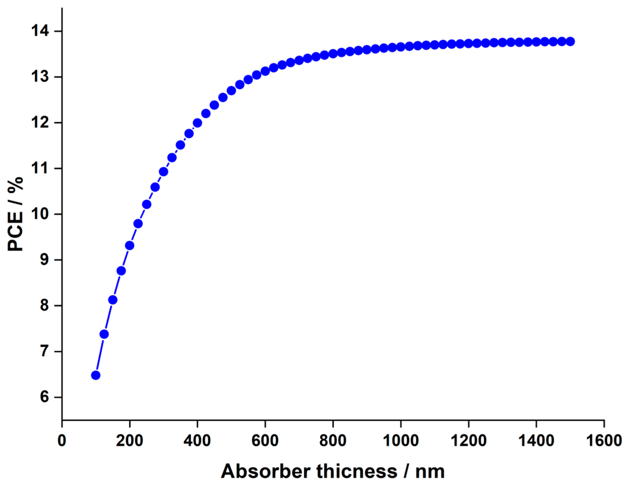
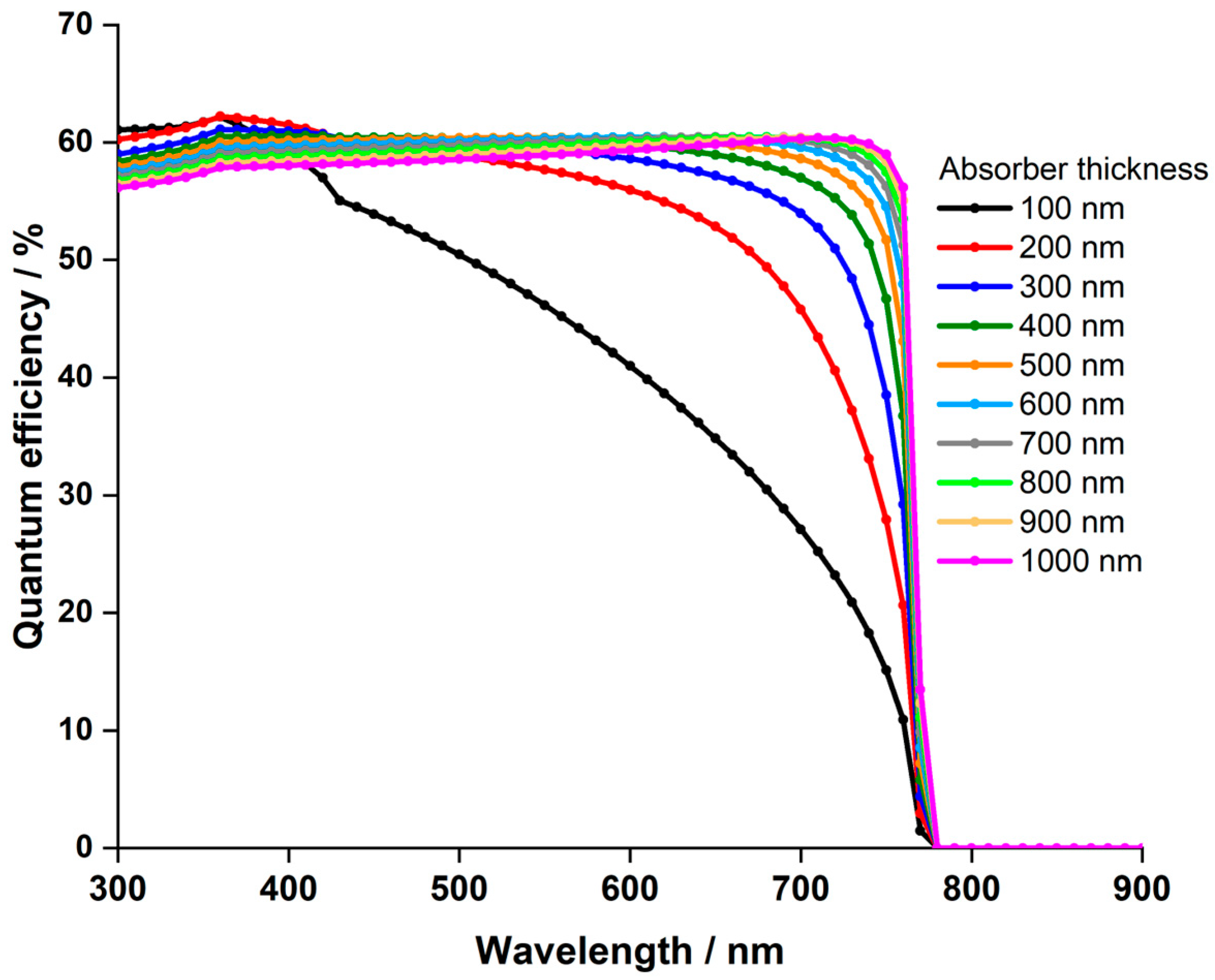
3.1.1. Impact of the LFDP Thickness
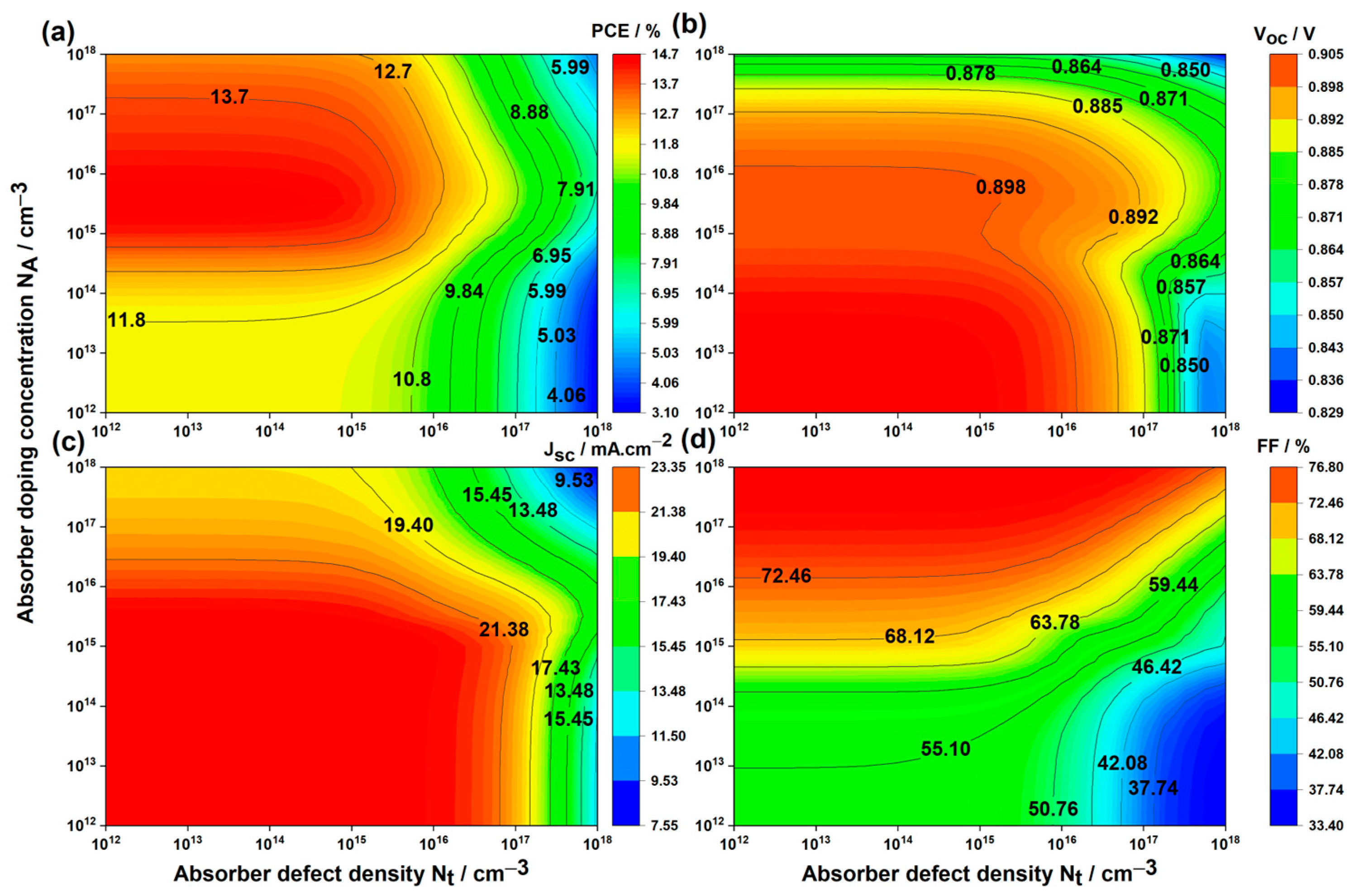
The performance of perovskite solar cells is heavily influenced by the thickness of the absorber layer, which directly affects the extent of light absorption and the efficiency of the conversion process. Maintaining an ideal thickness range is essential; if the layer is too thin, it might not absorb adequate light to produce sufficient current. On the contrary, an excessively thick absorber layer could impede the movement of charge carriers generated by absorbed light, making it challenging for them to travel through the material and reach the electrodes. This, in turn, results in reduced device efficiency. Striking the right balance in absorber layer thickness is critical for optimal solar cell performance.
In the experimental analyses, a hydrogenated C s 2 A g B i B r 6 layer with a thickness of 140 nm was utilized [44]. This section investigates the influence of absorber thickness on solar cell performance by adjusting the thickness within the range of 100 nm to 1500 nm. Figure 3 illustrates the J V characteristics for devices with thickness ranging from 100 nm to 1500 nm, and Figure 4 depicts the P C E in relation to the thickness variations.
The variation in V o c remains minimal and is independent of the thickness. However, J s c experiences a significant increase, rising from 10.29 to 23.31   m A . c m 2 as the thickness escalates from 100 to 700   n m . Consequently, this leads to a parallel rise in the P C E , escalating from 6.47% to 13.5% . Beyond 700   n m up to 1500   n m , J s c marginally increases, reaching 24.32   m A . c m 2 , while P C E only inches up to 13.75% , a mere 0.25% higher than the P C E at 700   n m , indicating a saturation point in P C E . The behavior described can be thoroughly analyzed through the external quantum efficiency curve of the cell at different thicknesses as a function of incident light wavelengths, depicted in Figure 5. The observed increasing trends in J s c and P C E in Figure 3 and Figure 4, respectively, as the absorber thickness increases up to 700   n m can be explained by enhanced light absorption. This aligns with the peak of quantum efficiency at this thickness in Figure 5.
Moreover, in Figure 5, it is apparent that quantum efficiency declines at wavelengths below 600   n m when the absorber thickness exceeds 700   n m , while it rises for longer wavelengths. Our study’s results match those of S. Dipta et al. [62], although they focused on a lead-based C H 3 N H 3 P b I 3 perovskite in their research. This pattern clarifies the saturated values of J s c and P C E observed for absorber thicknesses surpassing 700   n m . The high absorption coefficient of perovskite material at short wavelengths [63,64] leads to reduced quantum efficiency with thicker layers due to amplified light absorption. Thicker layers intensify the likelihood of absorbed photons generating electron-hole pairs, yet they may also elevate recombination events, wherein electron-hole pairs recombine before reaching the electrodes. This recombination diminishes quantum efficiency, especially at higher photon energies associated with shorter wavelengths.
Conversely, at longer wavelengths, the augmented quantum efficiency with increased thickness can be attributed to multiple factors. Thicker layers bolster the likelihood of light absorption, enabling more photons to be absorbed and creating electron-hole pairs. Moreover, at lower photon energies of longer wavelengths, recombination events are less probable. Hence, thicker layers enhance quantum efficiency, as a larger portion of absorbed photons contributes to charge carrier generation, minimizing losses from recombination processes.
In summary, the behavior of quantum efficiency in LFDP materials is shaped by the complex interactions among light absorption, recombination rates, and photon energy at various wavelengths and thicknesses. Based on these thorough findings, a thickness of 700   n m is chosen for the duration of this investigation.

3.1.2. Impact of Doping Concentration N A and Defect Density N t in the Absorber Layer

Choosing an appropriate absorber thickness is vital in solar cell design, but the defect density N t and acceptor doping concentration N A also play crucial roles. A higher defect density N t leads to increased defects, raising carrier recombination rates and negatively impacting device output [65,66]. Conversely, an increase in acceptor doping concentration N A has been correlated with improved overall solar cell performance [60].
In Figure 6, the variation of key parameters ( P C E , V o c , J s c , and F F ) in the C s 2 A g B i B r 6 -based PSC is depicted concerning absorber defect density N t (x-axis) and absorber doping concentration N A (y-axis), ranging from 10 12 to 10 18   c m 3 .
Below N t = 10 16   c m 3 , regardless of N A values, the PSC’s properties remained stable, but deterioration occurred when the defect density exceeded 10 16   c m 3 . Defects in the absorber layer act as recombination centers and trap states, reducing efficiency by limiting the number of carriers contributing to the electric current. These defects shorten carrier lifetimes, destabilize the material, and cause voltage losses. To enhance solar cell efficiency and reliability, minimizing defect density is essential. Studies have demonstrated that fabricating tin-based perovskite devices with defect density as low as N t = 10 15   c m 3 is achievable [60], making this the optimized value.
The absorber acceptor doping concentration N A significantly influences the P C E of the solar cell, as calculated using Equation (4), and is proportional to V o c , J s c , and F F .
P C E = V o c × J s c × F F P i n ,
where P i n is the incident power density in watts per square meter.
Analysis of Figure 6a indicates that the maximum PCE values are achieved within the doping concentration range of 10 12 to 10 18   c m 3 . This is attributed to the contradictory behavior of V o c and J s c on one hand, and F F on the other, concerning the doping concentration. Observations from Figure 6b,c reveal that V o c and J s c remain constant until N A reaches 10 16   c m 3 , after which they decrease. Contrarily, FF (Figure 6d) increases with higher doping concentrations. Our findings about how N A affects LFDP solar cell output perfectly match what Hui-Jing Du et al. discovered while studying lead-free C H 3 N H 3 S n I 3 CH3 [60].
Increasing acceptor doping boosts the concentration of free charge carriers, enhancing charge separation efficiency at the absorber/ETL interface. More photogenerated carriers contribute to V o c and J s c . However, as acceptor doping approaches ETL perovskite’s donor doping concentration N D = 10 18   c m 3 , charge recombination intensifies, reducing V o c and J s c . The proximity of acceptor and donor dopants accelerates charge recombination, diminishing device performance. However, F F , a dimensionless parameter representing the squareness of the current–voltage curve, is positively influenced by doping. Doping enhances absorber layer conductivity, facilitating efficient charge transport to electrodes and lowering series resistance, thereby improving F F . Additionally, doping affects shunt resistance, reducing unwanted current paths and leakage currents, further enhancing F F .
The interplay between enhanced conductivity, F F , and increased charge recombination, leading to decrease in V o c and J s c , influences P C E in perovskite solar cells. As acceptor doping concentrations of the absorber and donor doping concentration of the ETL approach each other, P C E decreases. It is crucial to balance enhanced conductivity and FF against charge recombination. The optimized value for N A = 10 16   c m 3 leads to a P C E of 14.52% , V o c of 0.898   V , J s c of 23.02   m A . c m 2 , and F F of 71.36% .

3.2. Influence of the HTL on LFDP Solar Cell Efficiency

In the context of (p-i-n) inverted structure PSCs, the HTL plays a pivotal role in ensuring the efficiency and stability of the device. It achieves this by enhancing charge extraction, reducing interfacial recombination, and modifying band alignment. Among the various HTL materials, Spiro-OMeTAD stands out due to its unique properties. Spiro-OMeTAD, with a bandgap of 2.9 eV, significantly enhances transparency, thereby minimizing optical losses before light penetrates the active double perovskite layer. Its excellent band alignment with the LFDP, coupled with good hole mobility, stability, ease of processing, and compatibility with flexible substrates, makes Spiro-OMeTAD an optimal choice for researchers and manufacturers dedicated to advancing perovskite solar cell technology. However, despite the remarkable properties of Spiro-OMeTAD, there is still room for improvement in the overall efficiency of PSCs. Specifically, optimization of the HTL thickness and doping concentration presents an avenue for enhancing the performance of these solar cells. These parameters demand meticulous exploration and adjustment to further elevate the efficiency and stability of Spiro-OMeTAD-based PSCs.

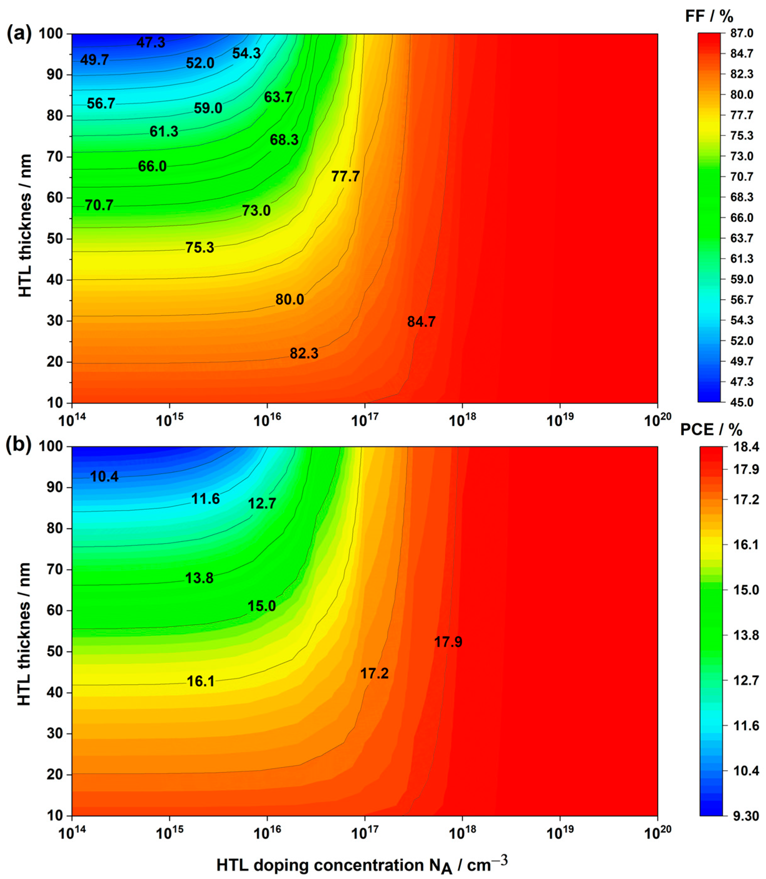
3.2.1. Impact of the HTL Thickness

Previous studies have underscored the critical influence of HTL thickness on PSC performance [67,68]. Strikingly, an ultra-thin HTL layer fails to completely cover the absorber layer. Conversely, a thick HTL layer heightens the risk of recombination due to the extended path length of charge carriers and increased electric resistance within the device. Thus, meticulous control of HTL thickness is paramount, aiming for full coverage of the uneven perovskite layer without escalating series resistance in the devices. Consequently, we conducted a study to identify the optimal HTL thickness. We varied the HTL thickness from 10 to 100   n m and scrutinized the photovoltaic performances. The initial thickness of Spiro-OmeTAd in the experimental work was 60   n m [44]. Figure 7 illustrates both the influence of HTL thickness on current density–voltage characteristics and its impact on F F and P C E . As depicted in Figure 7a, V o c remains constant across various thicknesses, while J s c marginally increases from 23.02   m A . c m 2 to 23.26   m A . c m 2 , ranging from 10   n m to 100   n m thickness. The substantial enhancement is observed in F F , as shown in Figure 7b, and consequently, in P C E , which is directly proportional to J s c and F F . F F elevates from 46.2% to 84.3% , leading to an increase in P C E from 9.55% to 17.7% . This improvement primarily stems from the fact that a thinner layer enhances light transparency, enabling more light to be absorbed by the LFDP layer. Consequently, more carriers are generated, augmenting J s c and F F , which essentially measures the device’s efficacy in converting incident light into electrical current. Additionally, a thinner layer reduces series resistance and improves charge collection efficiency. In a thin HTL, charges have a shorter distance to travel to reach the electrode, minimizing losses and enhancing F F .

3.2.2. Impact of the HTL Doping Concentration N A

Optimizing the performance of HTL involves considering not only the HTL thickness but also the doping concentration N A and its impact on photovoltaic parameters in PSCs. In the experimental study [44], a fixed doping concentration of N A = 1 × 10 15   c m 3 was utilized. However, our numerical analysis explored the effect of varying N A from 1 × 10 14 to 1 × 10 20   c m 3 while keeping the thickness constant at its original value of 60   n m . The results, as depicted in Figure 8, demonstrated comparable trends in photovoltaic metrics with variations in doping concentration, akin to the patterns observed with changes in HTL thickness (Figure 7).
Notably, for doping concentration, J s c , F F , and P C E increased with higher doping concentrations, contrasting the behaviour seen with increasing HTL thickness. Furthermore, it is noteworthy that V o c remained constant in both cases, indicating a consistent V o c across different doping concentrations (Figure 8a) and HTL thicknesses (Figure 7a). Specifically in Figure 8a, J s c marginally rose from 23.16   m A . c m 2 at N A = 1 × 10 14   c m 3 and 60   n m thickness to 23.26   m A . c m 2   23.33   m A . c m 2 at N A = 1 × 10 20   c m 3 with the same thickness. As depicted in Figure 8b, F F and consequently P C E exhibited a notable increase from 69.5% and 14.65% at N A = 1 × 10 14   c m 3 to 85.6% and 18% at N A = 1 × 10 18   c m 3 , after which both metrics approached saturation even with further increases in doping concentration to N A = 1 × 10 20   c m 3 . This enhancement in performance can be attributed to HTL doping, which enhances the mobility of charge carriers, particularly holes. Higher carrier mobility enables freer movement of charges within the material, reducing resistive losses and enhancing overall device conductivity. Doping also minimizes recombination by providing additional charge carriers to neutralize traps and defects within the material. Additionally, doping ensures appropriate energy level matching, thereby enhancing charge transfer efficiency.
In our pursuit of optimizing the HTL parameters for C s 2 A g B i B r 6 -based PSC, we delved into the relationship between HTL thickness and HTL doping concentration. Figure 9 illustrates the variations in P C E and F F in PSCs based on C s 2 A g B i B r 6 concerning HTL doping concentration (ranging from 1 × 10 14 to 1 × 10 20   c m 3 ) and HTL thickness (ranging from 10 to 100   n m ).
Notably, our findings reveal an inverse correlation between HTL thickness and doping concentration in inverted PSCs. Specifically, P C E and F F increased with higher doping concentration and decreased with thicker HTL thickness. It is noteworthy that an optimal balance exists; going below a thickness of 20   n m does not necessarily enhance cell performance, and an excessively high doping concentration, such as 1 × 10 20   c m 3 , is unnecessary. A concentration of 1 × 10 18   c m 3 suffices, especially considering the rising fabrication costs and complexity associated with higher doping levels [69]. Consequently, for the remainder of our study, we adopted an HTL thickness of 20   n m and a doping concentration of 1 × 10 18   c m 3 , resulting in impressive photovoltaic parameters: a P C E of 18.15% , V o c of 0.903   V , J s c of 23.27   m A . c m 2 , and F F of 86.56% .

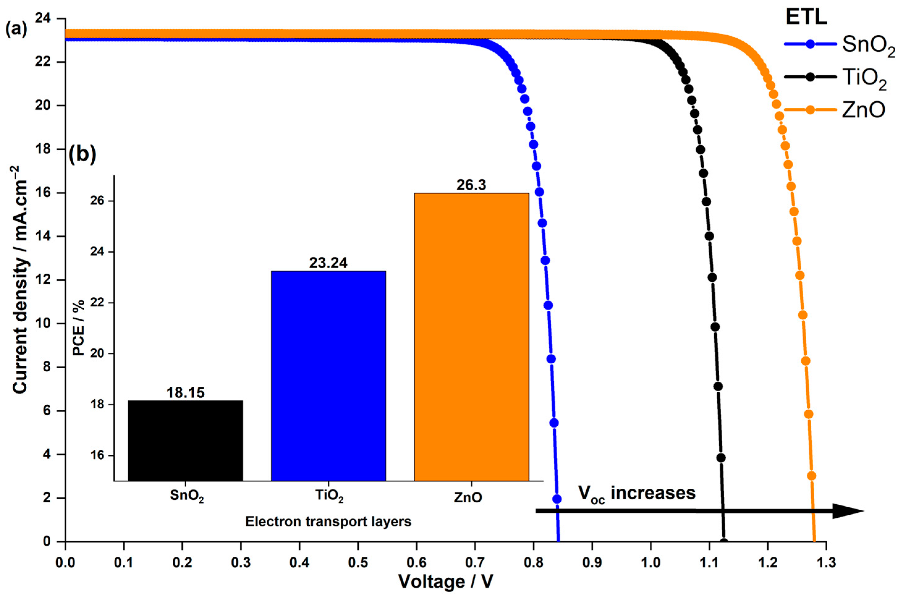
3.3. Influence of the ETL on LFDP Solar Cell Efficiency

Careful selection of ETL parameters is paramount in the design of high-performing solar cells, as emphasized in previous research [34]. ETLs within PSCs play vital roles, facilitating the collection and transfer of charge carriers following electron injection from the perovskite active layer. Of utmost significance is their ability to achieve effective charge separation and suppress charge carrier recombination. This intricate process hinges on optimizing factors such as the conduction band offset ( C B O ) and doping concentration. In this study, we investigate the influence of C B O on solar cell performance. Our analysis involves a comparative examination of the experimental structure used by Zhan et al. against two other cells utilizing the commonly employed metal oxides, titanium dioxide ( T i O 2 ) and zinc oxide (ZnO), as ETLs. Notably, we explore the photovoltaic outputs of these three devices, each with varying doping concentrations. Through this exploration, we gain valuable insights into the interplay between ETL parameters and the overall efficiency of PSCs, shedding light on the intricate mechanisms behind their optimal functioning.

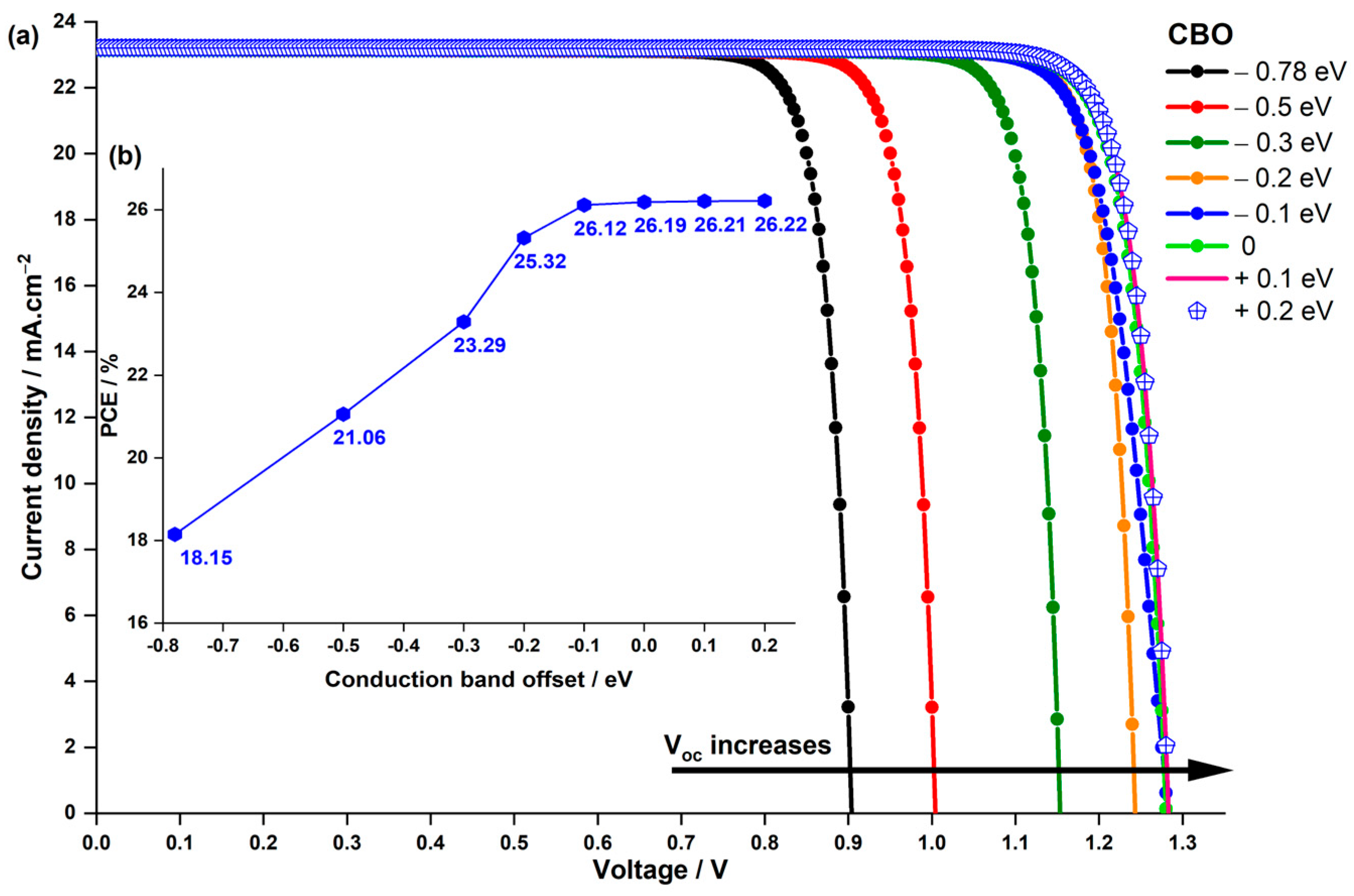
3.3.1. Impact of the CBO

Recently, extensive research efforts have been dedicated to finding suitable ETLs for PSCs to enhance charge carrier transport. This pursuit is driven by the fact that the V o c values below 1   V in most lead-free PSCs are insufficient when compared to the typical optical bandgap of the light absorber. The open-circuit losses in PSCs primarily stem from recombination processes within the perovskite bulk layer, as discussed in Section 3.1.2, and at the LFDP/ETL interface. To investigate the impact of the C B O between the LFDP and ETL, the back junction band alignment of the C s 2 A g B i B r 6 -based PSC was examined. C B O can be calculated using Equation (5), and its effect on the current density–voltage characteristics and PCE was explored.
C B O = χ A b s o r b e r χ E T L
In simulations where the ETL’s energy gap was constant at 3.6   e V , the CBO between the LFDP and ETL varied from 0.78   e V to 0.2   e V , achieved by altering the electron affinity χ E T L from −4.5 eV to −3.52 eV while maintaining a constant electron affinity of the absorber χ a b s o r b e r = 3.72   e V .  Figure 10 illustrates the results.
Notably, utilizing experimental values from Z. Zhang et al. [44], when the C B O between the LFDP and ETL was 0.78   e V , the corresponding cell exhibited the lowest V o c value of 0.903   V , resulting in the lowest P C E of 18.15% . However, as the C B O changed from 0.78 to 0   e V , the V o c significantly increased, leading to a higher P C E of 26.19% when χ E T L was equal to 3.72 eV (Figure 10b). After that, when C B O becomes positive, V o c and P C E saturate. It is also worth mentioning that J s c almost remains the same for all values of C B O .
This enhancement in V o c and consequently in P C E can be attributed to reducing the negative value of C B O . The negative C B O indicates that the energy level of the conduction band in the ETL is lower than that of the perovskite layer. Consequently, a larger energy barrier is created for electrons moving from the perovskite layer to the ETL, decreasing the built-in potential. Additionally, a negative C B O reduces the barrier for electron transport from the ETL’s conduction band to the interface. Since solar cell interfaces often have defect states, particularly deep defects that act as recombination centers for electrons and holes, a negative C B O exacerbates charge recombination through these interface deep-level defects. Given that V o c is essentially the built-in potential minus losses due to recombination and other factors, the increase in recombination at the interfaces due to negative C B O and the decrease in built-in potential resulted in a lower V o c and hence P C E .
In real-world applications, finding the right ETL is crucial, and among the promising options are Z n O and T i O 2 . T i O 2 has an electron affinity of 4.0   e V , resulting in a C B O of 0.2   e V , while Z n O , with an electron affinity of 3.7 eV, nearly approaches zero   C B O . These values represent significant improvements compared to the 0.78   e V   C B O observed between S n O 2 and the absorber material used in the study by Z. Zhang et al. [44]. To assess their performance, we simulated the J V characteristics and P C E for three different devices with varied ETLs, as depicted in Figure 11.
The finding suggests that devices incorporating the alternative T i O 2 and Z n O ETLs exhibited superior V o c and P C E compared to the original S n O 2 -based device. Notably, Z n O outperformed both S n O 2 and T i O 2 due to its excellent V o c of 1.27   V , resulting in an impressive 26.3%   P C E . These results can be attributed to the charge recombination at the interface explained previously, influenced by the C B O effect. Despite comparable electron mobility and conductivity among the proposed ETLs, their distinct alignment with the absorber material played a pivotal role in achieving these outcomes. Apart from the band alignment between the ETL and LFDP layer, their conductivity significantly influences cell design. Consequently, the performance of the optimized cell using S n O 2 as the ETL and the one employing Z n O as the ETL was compared under various doping concentrations.

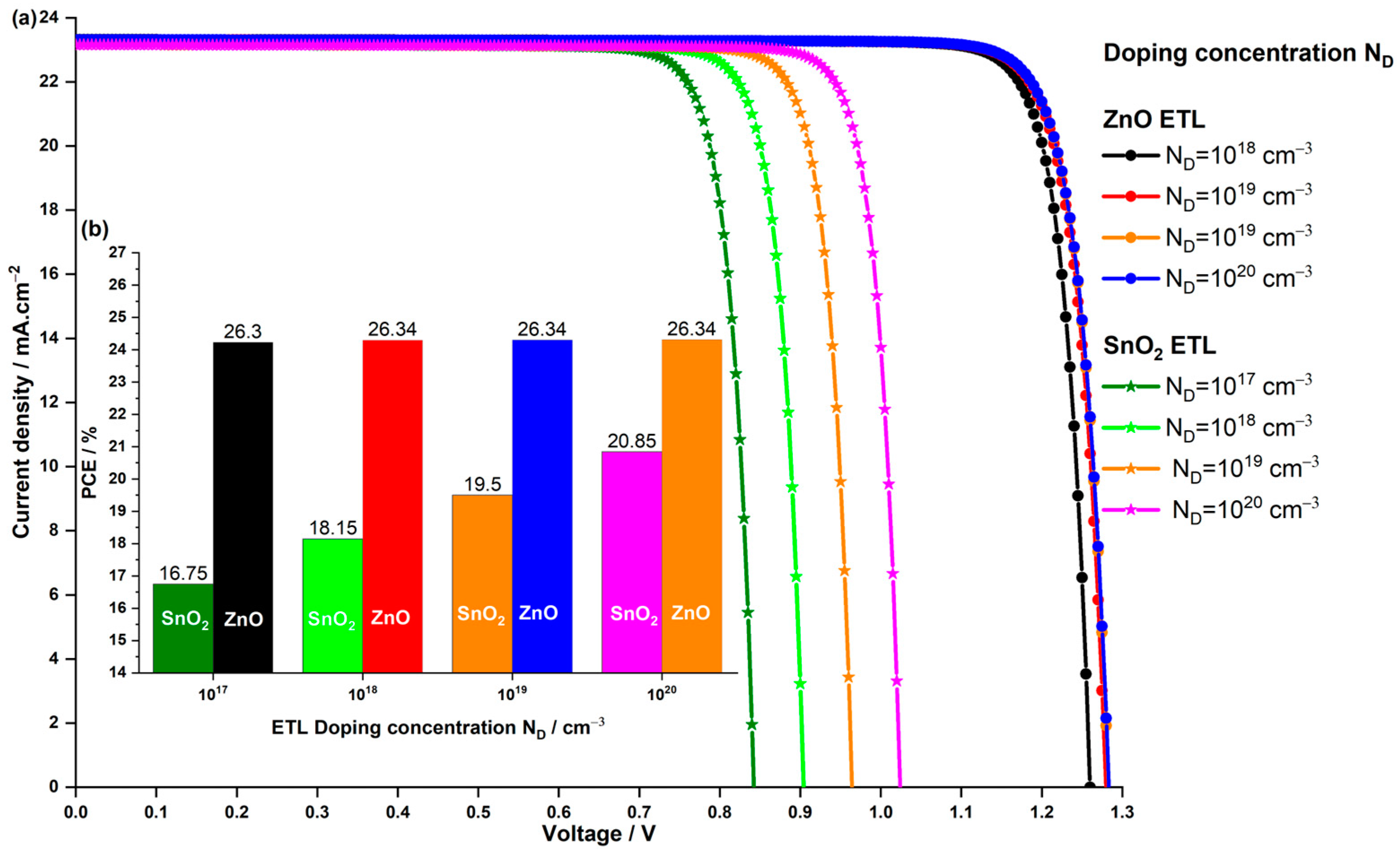
3.3.2. Impact of the ETL Doping Concentration N D

When dopants are introduced into the ETL, they can alter the charge carrier concentration and the conductivity of the material. This, in turn, affects the built-in electric field, which is crucial for separating and transporting electrons and holes within the solar cell. In our simulations, we varied the shallow donor doping concentration N D of the ETL from 1 × 10 17 to 1 × 10 20   c m 3 . We refrained from going below 1 × 10 17   c m 3 based on our findings in Section 3.1.2, where we observed that as the acceptor doping N A in the absorber approaches the donor doping concentration N D of the ETL, charge recombination intensifies, leading to a reduction in both V o c and J s c . Figure 12 illustrates the impact of donor doping concentration in both S n O 2 and Z n O ETLs on the J V characteristics and P C E of the solar cell.
In Figure 12a, it is evident that the J s c experiences a marginal increase with higher ETL doping concentrations for both devices utilizing different ETL materials. The most notable impact is observed in the V o c parameter, particularly in the solar cell employing S n O 2 ETL. For the Z n O ETL-based PSC, V o c rises with increasing Z n O doping concentration from 1 × 10 17 to 1 × 10 18   c m 3 , reaching a saturation point even if N D is increased to 1 × 10 20   c m 3 . In contrast, the S n O 2 ETL-based device exhibits a substantial effect, with V o c steadily increasing across the doping concentration range, rising from 0.842 V to 1.024 V for 1 × 10 17 to 1 × 10 20   c m 3 , respectively. In Figure 12b, the P C E trend mirrors that of V o c . The P C E of the Z n O ETL-based PSC sees a slight increase from 26.30% to 26.34%, while the S n O 2 ETL-based PSC continues to rise, reaching a maximum of 20.85%. Notably, even at the lowest doping concentration of 1 × 10 17   c m 3 , the P C E of the PSC with Z n O ETL surpasses that of the PSC with the original S n O 2 ETL used in Z. Zhan et al.’s experiment [44].
The significant enhancement in the S n O 2 ETL-based PSC’s performance is attributed to the association of increasing doping concentration with improved charge carrier transport properties and reduced recombination losses. As the doping concentration increases, electron mobility within the S n O 2 ETL improves, facilitating easier movement of electrons through the material, thereby reducing resistive losses and enhancing overall charge transport efficiency. Additionally, doping influences the energy levels and band alignment at the interfaces between different layers in the solar cell. Improved band alignment enhances the separation of photo-generated carriers, contributing to a higher open-circuit voltage. However, for the Z n O ETL-based PSC, which boasts six times better electron mobility than S n O 2 (as indicated in Table 1) and excellent band alignment with a C B O almost equal to zero, further increases in doping concentration may not significantly enhance the V o c of the PSC with Z n O ETL. Despite the advancements achieved with the S n O 2 ETL-based PSC, the device with Z n O remains the optimal choice, even at N D = 1 × 10 18   c m 3 , displaying a P C E of 26.34% , V o c of 1.278   V , J s c of 23.30   m A . c m 2 , and F F of 88.21% .

4. Conclusions

Although C s 2 A g B i B r 6 -based PSCs have been the subject of ground-breaking investigations, the obtained PCE has continuously dropped below 6.37%, falling short of the necessary threshold for commercial viability. Using SCAPS-1D software, we modeled an inverted (p-i-n) structure and carefully evaluated the performance of different parameter layers and materials for the ETL in our study. More specifically, we adjusted the thicknesses of the absorber and HTL, the doping concentrations of the absorber and HTL, and the absorber defect density. Additionally, we improved the efficiency of the solar cell by examining the impact of band alignment at the absorber/ETL interface and investigating the impacts of ETL doping on the device’s overall performance. We proposed Z n O as an optimal ETL alternative to S n O 2 , resulting in remarkable enhancements that culminated in an unprecedented P C E of nearly 26.34% , achieved using a lead-free double perovskite as the absorber layer. Looking forward, future research endeavors should focus on refining the techniques employed in device fabrication. Our innovative findings offer a promising avenue for developing cost-effective, highly efficient, and stable C s 2 A g B i B r 6 -based PSCs. These results underscore the significant potential of double perovskite solar cells for future commercial applications.

Author Contributions

Conceptualization, H.S.; methodology, H.S.; software, H.S.; validation, H.S.; formal analysis, H.S.; investigation, H.S.; resources, H.S.; data curation, H.S.; writing—original draft preparation, H.S.; writing—review and editing, H.S., Z.A.B., J.A. and R.M.; visualization, H.S., Z.A.B., J.A. and R.M.; supervision, H.S.; and project administration, H.S. All authors have read and agreed to the published version of the manuscript.

Funding

This research received no external funding.

Data Availability Statement

Data are contained within the article.

Acknowledgments

The author would like to acknowledge Marc Burgelman (University of Gent) for providing the simulation software SCAPS 3.8.

Conflicts of Interest

The authors declare no conflicts of interest.

References

  1. Shih, Y.-C.; Lan, Y.-B.; Li, C.-S.; Hsieh, H.-C.; Wang, L.; Wu, C.-I.; Lin, K.-F. Amino-Acid-Induced Preferential Orientation of Perovskite Crystals for Enhancing Interfacial Charge Transfer and Photovoltaic Performance. Small 2017, 13, 1604305. [Google Scholar] [CrossRef] [PubMed]
  2. Huang, H.-H.; Shih, Y.-C.; Wang, L.; Lin, K.-F. Boosting the Ultra-Stable Unencapsulated Perovskite Solar Cells by Using Montmorillonite/CH3NH3PbI3 Nanocomposite as Photoactive Layer. Energy Environ. Sci. 2019, 12, 1265–1273. [Google Scholar] [CrossRef]
  3. Yang, W.S.; Park, B.-W.; Jung, E.H.; Jeon, N.J.; Kim, Y.C.; Lee, D.U.; Shin, S.S.; Seo, J.; Kim, E.K.; Noh, J.H.; et al. Iodide Management in Formamidinium-Lead-Halide–Based Perovskite Layers for Efficient Solar Cells. Science 2017, 356, 1376–1379. [Google Scholar] [CrossRef] [PubMed]
  4. Zhong, M.; Zeng, W.; Tang, H.; Wang, L.-X.; Liu, F.-S.; Tang, B.; Liu, Q.-J. Band Structures, Effective Masses and Exciton Binding Energies of Perovskite Polymorphs of CH3NH3PbI3. Solar Energy 2019, 190, 617–621. [Google Scholar] [CrossRef]
  5. Wang, X.; Zhang, T.; Lou, Y.; Zhao, Y. All-Inorganic Lead-Free Perovskites for Optoelectronic Applications. Mater. Chem. Front. 2019, 3, 365–375. [Google Scholar] [CrossRef]
  6. Miyata, A.; Mitioglu, A.; Plochocka, P.; Portugall, O.; Wang, J.T.-W.; Stranks, S.D.; Snaith, H.J.; Nicholas, R.J. Direct Measurement of the Exciton Binding Energy and Effective Masses for Charge Carriers in Organic–Inorganic Tri-Halide Perovskites. Nature Phys. 2015, 11, 582–587. [Google Scholar] [CrossRef]
  7. Huang, J.; Yuan, Y.; Shao, Y.; Yan, Y. Understanding the Physical Properties of Hybrid Perovskites for Photovoltaic Applications. Nat. Rev. Mater. 2017, 2, 17042. [Google Scholar] [CrossRef]
  8. Jeon, N.J.; Na, H.; Jung, E.H.; Yang, T.-Y.; Lee, Y.G.; Kim, G.; Shin, H.-W.; Il Seok, S.; Lee, J.; Seo, J. A Fluorene-Terminated Hole-Transporting Material for Highly Efficient and Stable Perovskite Solar Cells. Nat. Energy 2018, 3, 682–689. [Google Scholar] [CrossRef]
  9. Yoo, J.J.; Seo, G.; Chua, M.R.; Park, T.G.; Lu, Y.; Rotermund, F.; Kim, Y.-K.; Moon, C.S.; Jeon, N.J.; Correa-Baena, J.-P.; et al. Efficient Perovskite Solar Cells via Improved Carrier Management. Nature 2021, 590, 587–593. [Google Scholar] [CrossRef]
  10. Jeong, J.; Kim, M.; Seo, J.; Lu, H.; Ahlawat, P.; Mishra, A.; Yang, Y.; Hope, M.A.; Eickemeyer, F.T.; Kim, M.; et al. Pseudo-Halide Anion Engineering for α-FAPbI3 Perovskite Solar Cells. Nature 2021, 592, 381–385. [Google Scholar] [CrossRef]
  11. Macdonald, T.J.; Batmunkh, M.; Lin, C.-T.; Kim, J.; Tune, D.D.; Ambroz, F.; Li, X.; Xu, S.; Sol, C.; Papakonstantinou, I.; et al. Origin of Performance Enhancement in TiO2-Carbon Nanotube Composite Perovskite Solar Cells. Small Methods 2019, 3, 1900164. [Google Scholar] [CrossRef]
  12. Saliba, M.; Correa-Baena, J.-P.; Wolff, C.M.; Stolterfoht, M.; Phung, N.; Albrecht, S.; Neher, D.; Abate, A. How to Make over 20% Efficient Perovskite Solar Cells in Regular (n–i–p) and Inverted (p–i–n) Architectures. Chem. Mater. 2018, 30, 4193–4201. [Google Scholar] [CrossRef]
  13. Jodlowski, A.D.; Roldán-Carmona, C.; Grancini, G.; Salado, M.; Ralaiarisoa, M.; Ahmad, S.; Koch, N.; Camacho, L.; de Miguel, G.; Nazeeruddin, M.K. Large Guanidinium Cation Mixed with Methylammonium in Lead Iodide Perovskites for 19% Efficient Solar Cells. Nat. Energy 2017, 2, 972–979. [Google Scholar] [CrossRef]
  14. Ng, C.H.; Lim, H.N.; Hayase, S.; Zainal, Z.; Huang, N.M. Photovoltaic Performances of Mono- and Mixed-Halide Structures for Perovskite Solar Cell: A Review. Renew. Sustain. Energy Rev. 2018, 90, 248–274. [Google Scholar] [CrossRef]
  15. Kung, P.-K.; Li, M.-H.; Lin, P.-Y.; Jhang, J.-Y.; Pantaler, M.; Lupascu, D.C.; Grancini, G.; Chen, P. Lead-Free Double Perovskites for Perovskite Solar Cells. Solar RRL 2020, 4, 1900306. [Google Scholar] [CrossRef]
  16. Xing, G.; Mathews, N.; Sun, S.; Lim, S.S.; Lam, Y.M.; Grätzel, M.; Mhaisalkar, S.; Sum, T.C. Long-Range Balanced Electron- and Hole-Transport Lengths in Organic-Inorganic CH3NH3PbI3. Science 2013, 342, 344–347. [Google Scholar] [CrossRef] [PubMed]
  17. Choi, H.; Jeong, J.; Kim, H.-B.; Kim, S.; Walker, B.; Kim, G.-H.; Kim, J.Y. Cesium-Doped Methylammonium Lead Iodide Perovskite Light Absorber for Hybrid Solar Cells. Nano Energy 2014, 7, 80–85. [Google Scholar] [CrossRef]
  18. Van Le, Q.; Jang, H.W.; Kim, S.Y. Recent Advances toward High-Efficiency Halide Perovskite Light-Emitting Diodes: Review and Perspective. Small Methods 2018, 2, 1700419. [Google Scholar] [CrossRef]
  19. Dou, L.; Yang, Y.; You, J.; Hong, Z.; Chang, W.-H.; Li, G.; Yang, Y. Solution-Processed Hybrid Perovskite Photodetectors with High Detectivity. Nat. Commun. 2014, 5, 5404. [Google Scholar] [CrossRef]
  20. Xu, J.; Saklatvala, R.; Mittal, S.; Deshmukh, S.; Procopio, A. Recent Progress of Potentiating Immune Checkpoint Blockade with External Stimuli—An Industry Perspective. Adv. Sci. 2020, 7, 1903394. [Google Scholar] [CrossRef]
  21. Yang, Y.; You, J. Make Perovskite Solar Cells Stable. Nature 2017, 544, 155–156. [Google Scholar] [CrossRef] [PubMed]
  22. Kopacic, I.; Friesenbichler, B.; Hoefler, S.F.; Kunert, B.; Plank, H.; Rath, T.; Trimmel, G. Enhanced Performance of Germanium Halide Perovskite Solar Cells through Compositional Engineering. ACS Appl. Energy Mater. 2018, 1, 343–347. [Google Scholar] [CrossRef]
  23. Shao, S.; Liu, J.; Portale, G.; Fang, H.-H.; Blake, G.R.; ten Brink, G.H.; Koster, L.J.A.; Loi, M.A. Highly Reproducible Sn-Based Hybrid Perovskite Solar Cells with 9% Efficiency. Adv. Energy Mater. 2018, 8, 1702019. [Google Scholar] [CrossRef]
  24. Yang, D.; Lv, J.; Zhao, X.; Xu, Q.; Fu, Y.; Zhan, Y.; Zunger, A.; Zhang, L. Functionality-Directed Screening of Pb-Free Hybrid Organic–Inorganic Perovskites with Desired Intrinsic Photovoltaic Functionalities. Chem. Mater. 2017, 29, 524–538. [Google Scholar] [CrossRef]
  25. Hao, F.; Stoumpos, C.C.; Cao, D.H.; Chang, R.P.H.; Kanatzidis, M.G. Lead-Free Solid-State Organic–Inorganic Halide Perovskite Solar Cells. Nat. Photon 2014, 8, 489–494. [Google Scholar] [CrossRef]
  26. Sabbah, H.; Baki, Z.A. Device Simulation of Highly Stable and 29% Efficient FA0.75MA0.25Sn0.95Ge0.05I3-Based Perovskite Solar Cell. Nanomaterials 2023, 13, 1537. [Google Scholar] [CrossRef]
  27. Nasti, G.; Abate, A. Tin Halide Perovskite (ASnX3) Solar Cells: A Comprehensive Guide toward the Highest Power Conversion Efficiency. Adv. Energy Mater. 2020, 10, 1902467. [Google Scholar] [CrossRef]
  28. Stoumpos, C.C.; Malliakas, C.D.; Kanatzidis, M.G. Semiconducting Tin and Lead Iodide Perovskites with Organic Cations: Phase Transitions, High Mobilities, and Near-Infrared Photoluminescent Properties. Inorg. Chem. 2013, 52, 9019–9038. [Google Scholar] [CrossRef]
  29. Tong, J.; Gong, J.; Hu, M.; Yadavalli, S.K.; Dai, Z.; Zhang, F.; Xiao, C.; Hao, J.; Yang, M.; Anderson, M.A.; et al. High-Performance Methylammonium-Free Ideal-Band-Gap Perovskite Solar Cells. Matter 2021, 4, 1365–1376. [Google Scholar] [CrossRef]
  30. Rühle, S. Tabulated Values of the Shockley–Queisser Limit for Single Junction Solar Cells. Solar Energy 2016, 130, 139–147. [Google Scholar] [CrossRef]
  31. Wang, C.; Zhang, Y.; Gu, F.; Zhao, Z.; Li, H.; Jiang, H.; Bian, Z.; Liu, Z. Illumination Durability and High-Efficiency Sn-Based Perovskite Solar Cell under Coordinated Control of Phenylhydrazine and Halogen Ions. Matter 2021, 4, 709–721. [Google Scholar] [CrossRef]
  32. Arayro, J.; Mezher, R.; Sabbah, H. Comparative Simulation Study of the Performance of Conventional and Inverted Hybrid Tin-Based Perovskite Solar Cells. Coatings 2023, 13, 1258. [Google Scholar] [CrossRef]
  33. Byranvand, M.M.; Zuo, W.; Imani, R.; Pazoki, M.; Saliba, M. Tin-Based Halide Perovskite Materials: Properties and Applications. Chem. Sci. 2022, 13, 6766–6781. [Google Scholar] [CrossRef] [PubMed]
  34. Giustino, F.; Snaith, H.J. Toward Lead-Free Perovskite Solar Cells. ACS Energy Lett. 2016, 1, 1233–1240. [Google Scholar] [CrossRef]
  35. Wei, F.; Deng, Z.; Sun, S.; Zhang, F.; Evans, D.M.; Kieslich, G.; Tominaka, S.; Carpenter, M.A.; Zhang, J.; Bristowe, P.D.; et al. Synthesis and Properties of a Lead-Free Hybrid Double Perovskite: (CH3NH3)2AgBiBr6. Chem. Mater. 2017, 29, 1089–1094. [Google Scholar] [CrossRef]
  36. Creutz, S.E.; Crites, E.N.; De Siena, M.C.; Gamelin, D.R. Colloidal Nanocrystals of Lead-Free Double-Perovskite (Elpasolite) Semiconductors: Synthesis and Anion Exchange To Access New Materials. Nano Lett. 2018, 18, 1118–1123. [Google Scholar] [CrossRef]
  37. Slavney, A.H.; Hu, T.; Lindenberg, A.M.; Karunadasa, H.I. A Bismuth-Halide Double Perovskite with Long Carrier Recombination Lifetime for Photovoltaic Applications. J. Am. Chem. Soc. 2016, 138, 2138–2141. [Google Scholar] [CrossRef]
  38. McClure, E.T.; Ball, M.R.; Windl, W.; Woodward, P.M. Cs2AgBiX6 (X = Br, Cl): New Visible Light Absorbing, Lead-Free Halide Perovskite Semiconductors. Chem. Mater. 2016, 28, 1348–1354. [Google Scholar] [CrossRef]
  39. Savory, C.N.; Walsh, A.; Scanlon, D.O. Can Pb-Free Halide Double Perovskites Support High-Efficiency Solar Cells? ACS Energy Lett. 2016, 1, 949–955. [Google Scholar] [CrossRef]
  40. Wang, M.; Zeng, P.; Bai, S.; Gu, J.; Li, F.; Yang, Z.; Liu, M. High-Quality Sequential-Vapor-Deposited Cs2AgBiBr6 Thin Films for Lead-Free Perovskite Solar Cells. Solar RRL 2018, 2, 1800217. [Google Scholar] [CrossRef]
  41. Wang, B.; Li, N.; Yang, L.; Dall’Agnese, C.; Jena, A.K.; Miyasaka, T.; Wang, X.-F. Organic Dye/Cs2AgBiBr6 Double Perovskite Heterojunction Solar Cells. J. Am. Chem. Soc. 2021, 143, 14877–14883. [Google Scholar] [CrossRef] [PubMed]
  42. Gao, W.; Ran, C.; Xi, J.; Jiao, B.; Zhang, W.; Wu, M.; Hou, X.; Wu, Z. High-Quality Cs2AgBiBr6 Double Perovskite Film for Lead-Free Inverted Planar Heterojunction Solar Cells with 2.2% Efficiency. ChemPhysChem 2018, 19, 1696–1700. [Google Scholar] [CrossRef] [PubMed]
  43. Sirtl, M.T.; Hooijer, R.; Armer, M.; Ebadi, F.G.; Mohammadi, M.; Maheu, C.; Weis, A.; van Gorkom, B.T.; Häringer, S.; Janssen, R.A.J.; et al. 2D/3D Hybrid Cs2AgBiBr6 Double Perovskite Solar Cells: Improved Energy Level Alignment for Higher Contact-Selectivity and Large Open Circuit Voltage. Adv. Energy Mater. 2022, 12, 2103215. [Google Scholar] [CrossRef]
  44. Zhang, Z.; Sun, Q.; Lu, Y.; Lu, F.; Mu, X.; Wei, S.-H.; Sui, M. Hydrogenated Cs2AgBiBr6 for Significantly Improved Efficiency of Lead-Free Inorganic Double Perovskite Solar Cell. Nat. Commun. 2022, 13, 3397. [Google Scholar] [CrossRef] [PubMed]
  45. Minemoto, T.; Murata, M. Theoretical Analysis on Effect of Band Offsets in Perovskite Solar Cells. Sol. Energy Mater. Sol. Cells 2015, 133, 8–14. [Google Scholar] [CrossRef]
  46. Liu, F.; Zhu, J.; Wei, J.; Li, Y.; Lv, M.; Yang, S.; Zhang, B.; Yao, J.; Dai, S. Numerical Simulation: Toward the Design of High-Efficiency Planar Perovskite Solar Cells. Appl. Phys. Lett. 2014, 104, 253508. [Google Scholar] [CrossRef]
  47. Sabbah, H. Numerical Simulation of 30% Efficient Lead-Free Perovskite CsSnGeI3-Based Solar Cells. Materials 2022, 15, 3229. [Google Scholar] [CrossRef]
  48. Liu, Y.; Heinzel, D.; Rockett, A. A New Solar Cell Simulator: WxAMPS. In Proceedings of the 2011 37th IEEE Photovoltaic Specialists Conference, Seattle, WA, USA, 19–24 June 2011; pp. 002753–002756. [Google Scholar]
  49. Burgelman, M.; Nollet, P.; Degrave, S. Modelling Polycrystalline Semiconductor Solar Cells. Thin Solid. Films 2000, 361–362, 527–532. [Google Scholar] [CrossRef]
  50. Islam, T.; Jani, R.; Amin, S.M.A.; Shorowordi, K.M.; Nishat, S.S.; Kabir, A.; Taufique, M.F.N.; Chowdhury, S.; Banerjee, S.; Ahmed, S. Simulation Studies to Quantify the Impacts of Point Defects: An Investigation of Cs2AgBiBr6 Perovskite Solar Devices Utilizing ZnO and Cu2O as the Charge Transport Layers. Comput. Mater. Sci. 2020, 184, 109865. [Google Scholar] [CrossRef]
  51. Mohandes, A.; Moradi, M.; Nadgaran, H. Numerical Simulation of Inorganic Cs2AgBiBr6 as a Lead-Free Perovskite Using Device Simulation SCAPS-1D. Opt. Quant. Electron. 2021, 53, 319. [Google Scholar] [CrossRef]
  52. Liu, G.; Zhong, Y.; Mao, H.; Yang, J.; Dai, R.; Hu, X.; Xing, Z.; Sheng, W.; Tan, L.; Chen, Y. Highly Efficient and Stable ZnO-Based MA-Free Perovskite Solar Cells via Overcoming Interfacial Mismatch and Deprotonation Reaction. Chem. Eng. J. 2022, 431, 134235. [Google Scholar] [CrossRef]
  53. Raj, A.; Kumar, M.; Kumar, A.; Laref, A.; Singh, K.; Sharma, S.; Anshul, A. Effect of Doping Engineering in TiO2 Electron Transport Layer on Photovoltaic Performance of Perovskite Solar Cells. Mater. Lett. 2022, 313, 131692. [Google Scholar] [CrossRef]
  54. Hosseini, S.R.; Bahramgour, M.; Yardani Sefidi, P.; Tabatabaei Mashayekh, A.; Moradi, A.; Delibas, N.; Hosseini, M.G.; Niaei, A. Investigating the Effect of Non-Ideal Conditions on the Performance of a Planar CH3NH3PbI3-Based Perovskite Solar Cell through SCAPS-1D Simulation. Heliyon 2022, 8, e11471. [Google Scholar] [CrossRef] [PubMed]
  55. Seyed-Talebi, S.M.; Mahmoudi, M.; Lee, C.-H. A Comprehensive Study of CsSnI3-Based Perovskite Solar Cells with Different Hole Transporting Layers and Back Contacts. Micromachines 2023, 14, 1562. [Google Scholar] [CrossRef] [PubMed]
  56. Baena, J.P.C.; Steier, L.; Tress, W.; Saliba, M.; Neutzner, S.; Matsui, T.; Giordano, F.; Jacobsson, T.J.; Kandada, A.R.S.; Zakeeruddin, S.M.; et al. Highly Efficient Planar Perovskite Solar Cells through Band Alignment Engineering. Energy Environ. Sci. 2015, 8, 2928–2934. [Google Scholar] [CrossRef]
  57. Vasheghani Farahani, S.K.; Veal, T.D.; Mudd, J.J.; Scanlon, D.O.; Watson, G.W.; Bierwagen, O.; White, M.E.; Speck, J.S.; McConville, C.F. Valence-Band Density of States and Surface Electron Accumulation in Epitaxial SnO2 Films. Phys. Rev. B 2014, 90, 155413. [Google Scholar] [CrossRef]
  58. Doroody, C.; Rahman, K.S.; Rosly, H.N.; Harif, M.N.; Haque, F.; Tiong, S.K.; Amin, N. Impact of High Resistivity Transparent (HRT) Layer in Cadmium Telluride Solar Cells from Numerical Simulation. J. Renew. Sustain. Energy 2020, 12, 023702. [Google Scholar] [CrossRef]
  59. Hoye, R.L.Z.; Ehrler, B.; Böhm, M.L.; Muñoz-Rojas, D.; Altamimi, R.M.; Alyamani, A.Y.; Vaynzof, Y.; Sadhanala, A.; Ercolano, G.; Greenham, N.C.; et al. Improved Open-Circuit Voltage in ZnO–PbSe Quantum Dot Solar Cells by Understanding and Reducing Losses Arising from the ZnO Conduction Band Tail. Adv. Energy Mater. 2014, 4, 1301544. [Google Scholar] [CrossRef]
  60. Du, H.-J.; Wang, W.-C.; Zhu, J.-Z. Device Simulation of Lead-Free CH3NH3SnI3 Perovskite Solar Cells with High Efficiency. Chin. Phys. B 2016, 25, 108802. [Google Scholar] [CrossRef]
  61. Stamate, M.D. On the Dielectric Properties of Dc Magnetron TiO2 Thin Films. Appl. Surf. Sci. 2003, 218, 318–323. [Google Scholar] [CrossRef]
  62. Dipta, S.S.; Uddin, A.; Conibeer, G. Enhanced Light Management and Optimization of Perovskite Solar Cells Incorporating Wavelength Dependent Reflectance Modeling. Heliyon 2022, 8, e11380. [Google Scholar] [CrossRef] [PubMed]
  63. Shaikh, M.N.; Zafar, Q.; Papadakis, A. A Study of Electromagnetic Light Propagation in a Perovskite-Based Solar Cell via a Computational Modelling Approach. Bull. Mater. Sci. 2019, 42, 169. [Google Scholar] [CrossRef]
  64. Chander, N.; Khan, A.F.; Chandrasekhar, P.S.; Thouti, E.; Swami, S.K.; Dutta, V.; Komarala, V.K. Reduced Ultraviolet Light Induced Degradation and Enhanced Light Harvesting Using YVO4:Eu3+ down-Shifting Nano-Phosphor Layer in Organometal Halide Perovskite Solar Cells. Appl. Phys. Lett. 2014, 105, 033904. [Google Scholar] [CrossRef]
  65. Haider, S.Z.; Anwar, H.; Wang, M. A Comprehensive Device Modelling of Perovskite Solar Cell with Inorganic Copper Iodide as Hole Transport Material. Semicond. Sci. Technol. 2018, 33, 035001. [Google Scholar] [CrossRef]
  66. Karimi, E.; Ghorashi, S.M.B. Investigation of the Influence of Different Hole-Transporting Materials on the Performance of Perovskite Solar Cells. Optik 2017, 130, 650–658. [Google Scholar] [CrossRef]
  67. Sabbah, H.; Arayro, J.; Mezher, R. Numerical Simulation and Optimization of Highly Stable and Efficient Lead-Free Perovskite FA1−xCsxSnI3-Based Solar Cells Using SCAPS. Materials 2022, 15, 4761. [Google Scholar] [CrossRef]
  68. Arumugam, G.M.; Karunakaran, S.K.; Liu, C.; Zhang, C.; Guo, F.; Wu, S.; Mai, Y. Inorganic Hole Transport Layers in Inverted Perovskite Solar Cells: A Review. Nano Select 2021, 2, 1081–1116. [Google Scholar] [CrossRef]
  69. Li, S.; Cao, Y.-L.; Li, W.-H.; Bo, Z.-S. A Brief Review of Hole Transporting Materials Commonly Used in Perovskite Solar Cells. Rare Met. 2021, 40, 2712–2729. [Google Scholar] [CrossRef]
Figure 1. Schematic diagram of C s 2 A g B i B r 6 -based PSC.
Nanomaterials 14 00048 g001
Figure 2. Comparison of current density (J–V curve) between simulation results (depicted in dark blue) and experimental findings (illustrated in orange).
Nanomaterials 14 00048 g002
Figure 3. Impact of absorber thickness on J–V characteristics of C s 2 A g B i B r 6 -based PSC.
Nanomaterials 14 00048 g003
Figure 4. Change in   P C E as function of absorber thickness in C s 2 A g B i B r 6 -based PSC.
Nanomaterials 14 00048 g004
Figure 5. The effect of absorber thickness on the quantum efficiency of C s 2 A g B i B r 6 -based PSC.
Nanomaterials 14 00048 g005
Figure 6. Variations in solar cell performance based on absorber defect densities and absorber doping concentration: (a) P C E , (b) V o c , (c) J s c , and (d) F F .
Nanomaterials 14 00048 g006
Figure 7. Effect of HTL thickness on (a) the current density–voltage characteristics of the PSC, and (b) the PCE and FF.
Nanomaterials 14 00048 g007
Figure 8. Effect of HTL doping concentration on (a) the current density–voltage characteristics of the PSC, and (b) the PCE and FF.
Nanomaterials 14 00048 g008
Figure 9. Variations in solar cell performance based on HTL doping concentration and HTL thickness: (a) F F and (b) P C E .
Nanomaterials 14 00048 g009
Figure 10. Impact of CBO on (a) the current density–voltage characteristics of the PSC and (b) the PCE.
Nanomaterials 14 00048 g010
Figure 11. Impact of the ETL material on (a) the current density–voltage characteristics of the PSC and (b) the PCE.
Nanomaterials 14 00048 g011
Figure 12. Impact of the doping concentration of the S n O 2 and Z n O ETL on the (a) the current density–voltage characteristics of the PSC and (b) the PCE.
Nanomaterials 14 00048 g012
Table 1. Electrical and optical properties used in simulation of a LFDP based on C s 2 A g B i B r 6 .
ParametersSpiro-OMeTAD (HTL)
[44,54,55]
C s 2 A g B i B r 6
(Absorber) [44,51]
S n O 2
(ETL) [44,56,57]
Z n O
(ETL) [58,59]
T i O 2
(ETL)
[60,61]
Thickness ( µ m ) 0.060 0.140 0.050 0.05 0.050
Bandgap E g (eV) 2.9 1.61 3.6 3.3 3.26
Electron affinity χ (eV) 2.2 3.72 4.5 3.7 4
Dielectric permittivity 3 5.8 8 9 32
CB effective density
of states ( c m 3 )
2.5 × 10 19 2 × 10 18 2.2 × 10 18 2.2 × 10 18 2.2 × 10 18
VB effective density
of states ( c m 3 )
1.8 × 10 19 1 × 10 18 1.8 × 10 19 1.8 × 10 19 1.8 × 10 19
Electron mobility
( c m 2 / V . s )
2 × 10 4 9.28 15 100 20
Hole mobility
( c m 2 / V . s )
2 × 10 4 9.28 15 25 10
Donor concentration
N D ( c m 3 )
1 × 10 7 0 1 × 10 18 1 × 10 18 1 × 10 18
Acceptor concentration N A ( c m 3 ) 1 × 10 15 1 × 10 15 0 0 0
Table 2. Density values of defects within cell layers and at the cell interface.
ParametersETLHTLAbsorberHTL/AbsorberAbsorber/ETL
Defect TypeNeutralNeutralNeutralNeutralNeutral
Capture cross-section
for electrons σ n   ( c m 2 )
1 × 10 15 1 × 10 15 1 × 10 15 1 × 10 18 1 × 10 15
Capture cross-section
for hole σ p   ( c m 2 )
1 × 10 15 1 × 10 15 1 × 10 15 1 × 10 16 1 × 10 15
Energetic distributionSingleSingleGaussianSingleSingle
Energy level with respect to E v (above E v ) (eV)0.60.6500.60.60.6
Characteristic energy (eV)0.10.10.10.10.1
Total density N t   ( c m 3 ) 1 × 10 15 1 × 10 15 1 × 10 16 1 × 10 12 1 × 10 12
Disclaimer/Publisher’s Note: The statements, opinions and data contained in all publications are solely those of the individual author(s) and contributor(s) and not of MDPI and/or the editor(s). MDPI and/or the editor(s) disclaim responsibility for any injury to people or property resulting from any ideas, methods, instructions or products referred to in the content.

