
Design and Analysis of Gallium Arsenide-Based Nanowire Using Coupled Non-Equilibrium Green Function for RF Hybrid Applications


Abstract
1. Introduction
2. Basics of NEGF Modeling
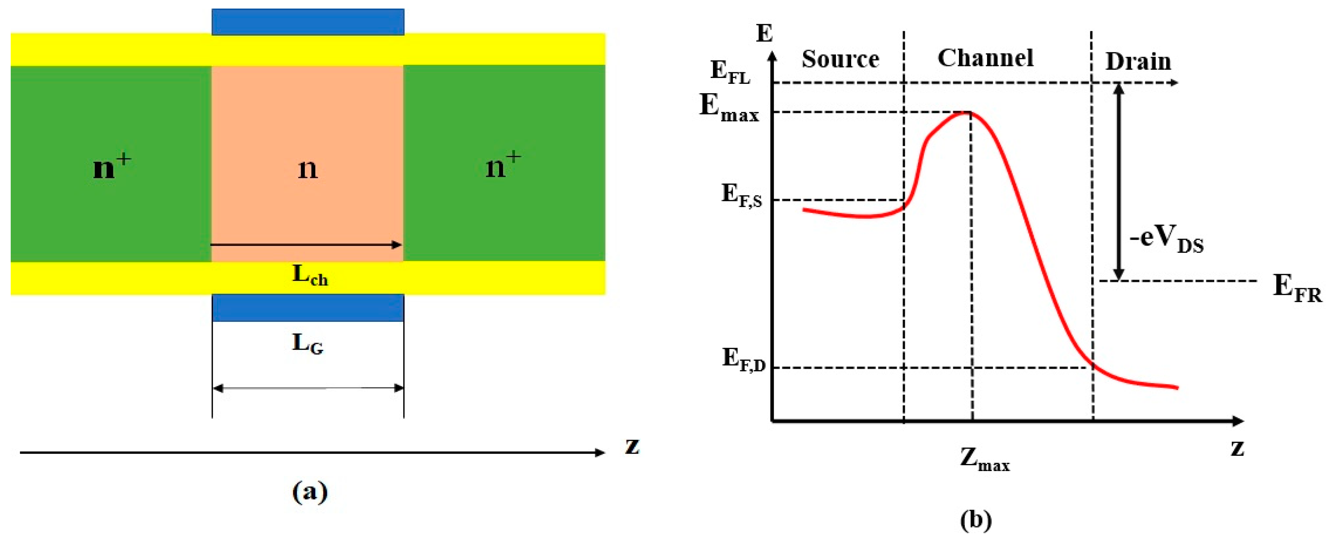
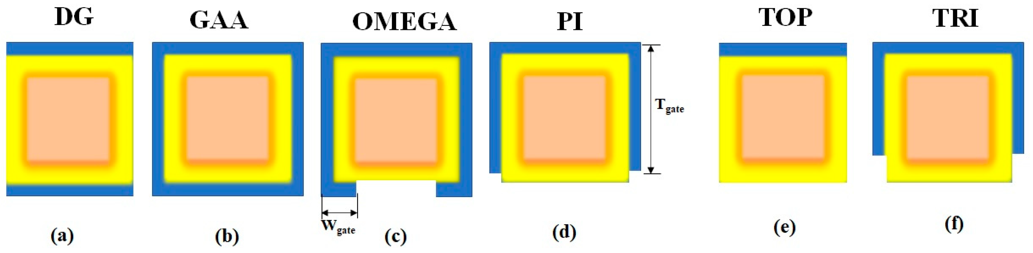
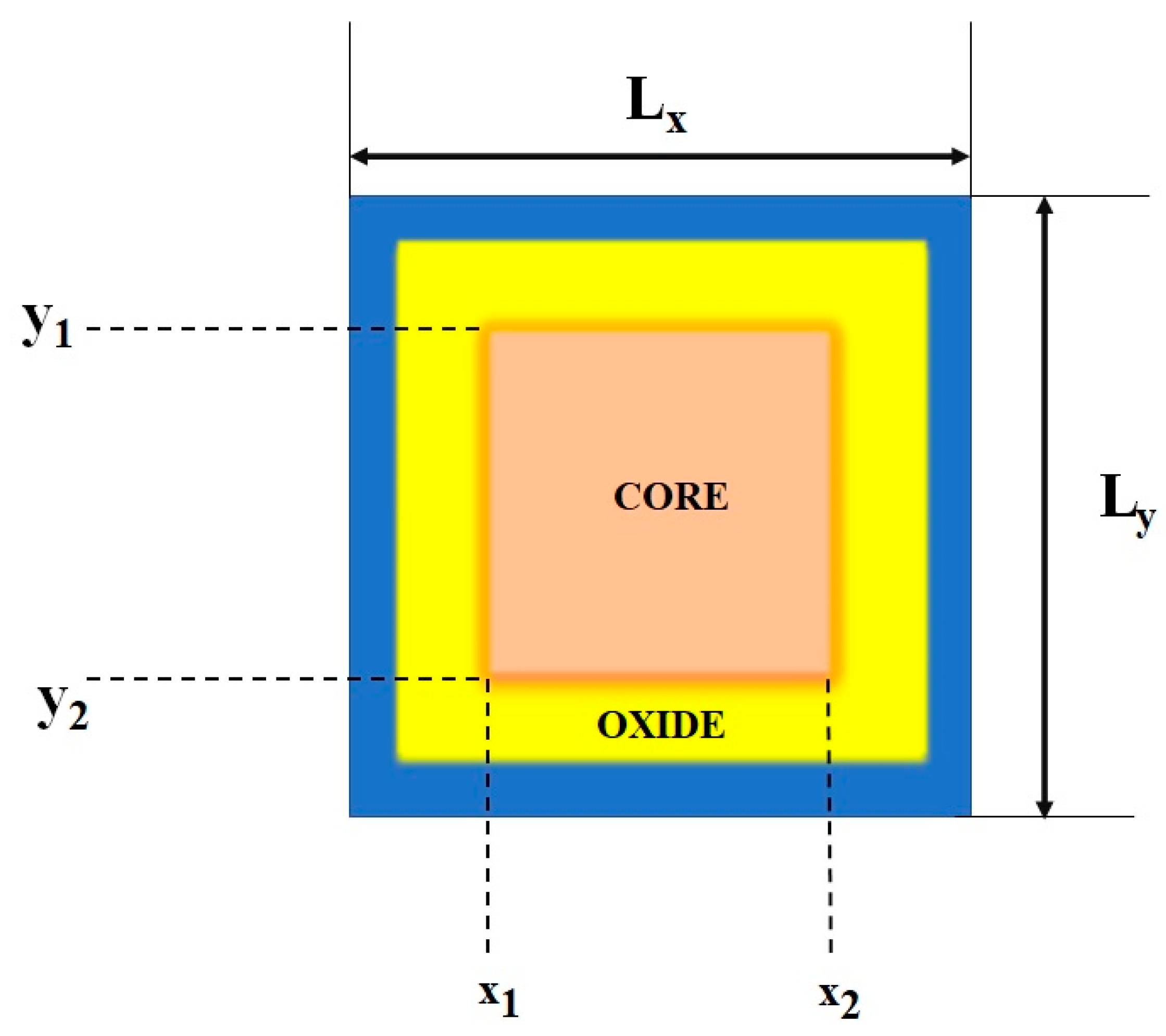
3. Design of Proposed Novel GaAs Nanowire
4. Mathematical Modeling of the Nanowire with La2O3
4.1. Numerical Approaches
4.1.1. K-Space Solutions of Two-Dimensional Schrodinger Equations
4.1.2. Product Space Solutions of 2-D Schrodinger Equations
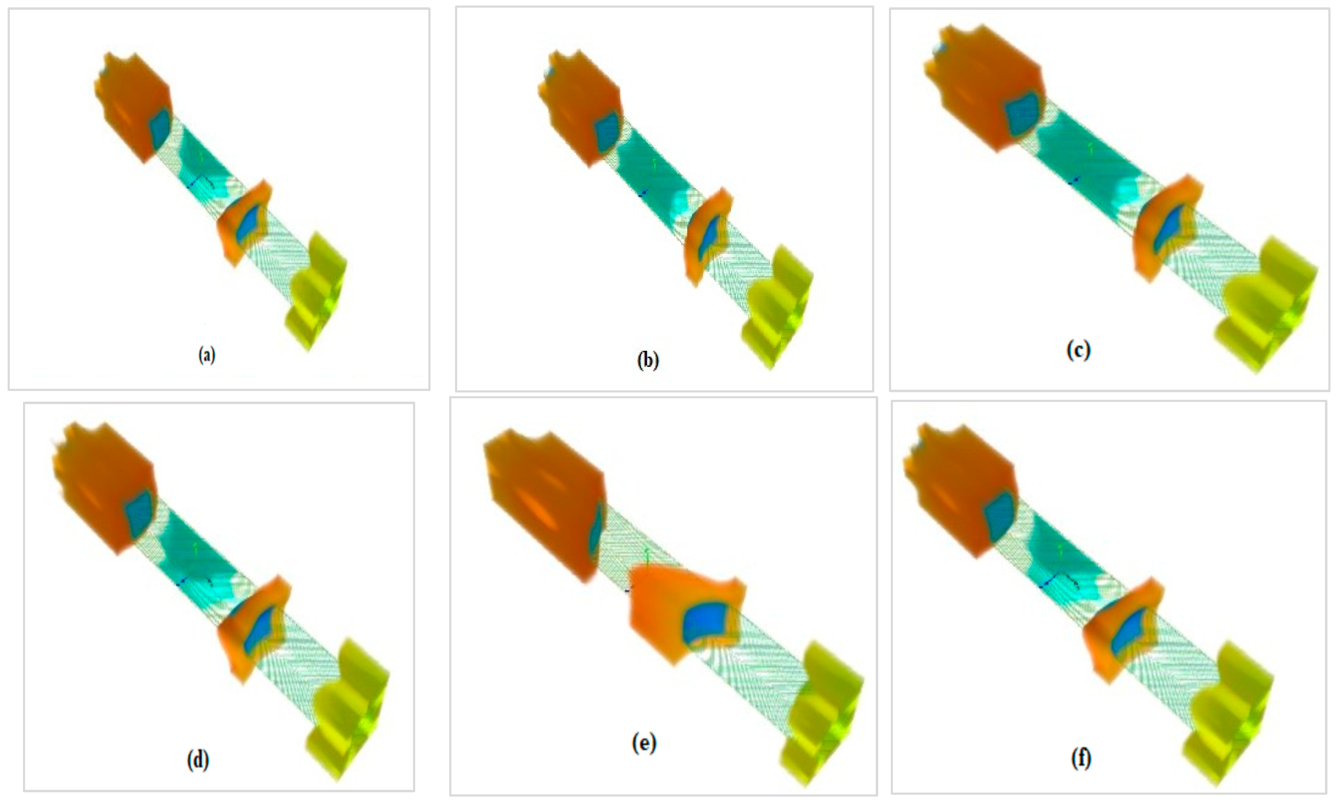
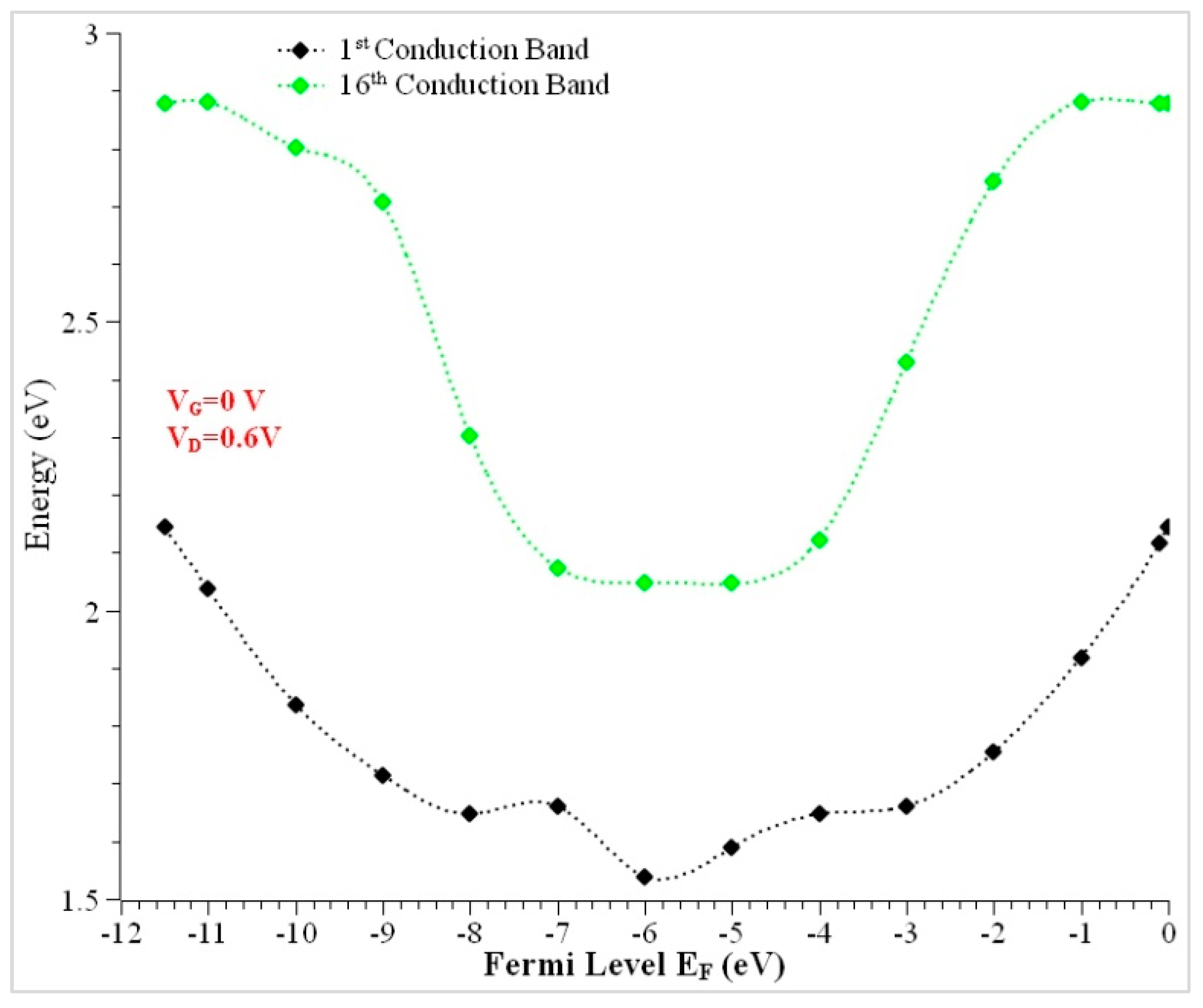
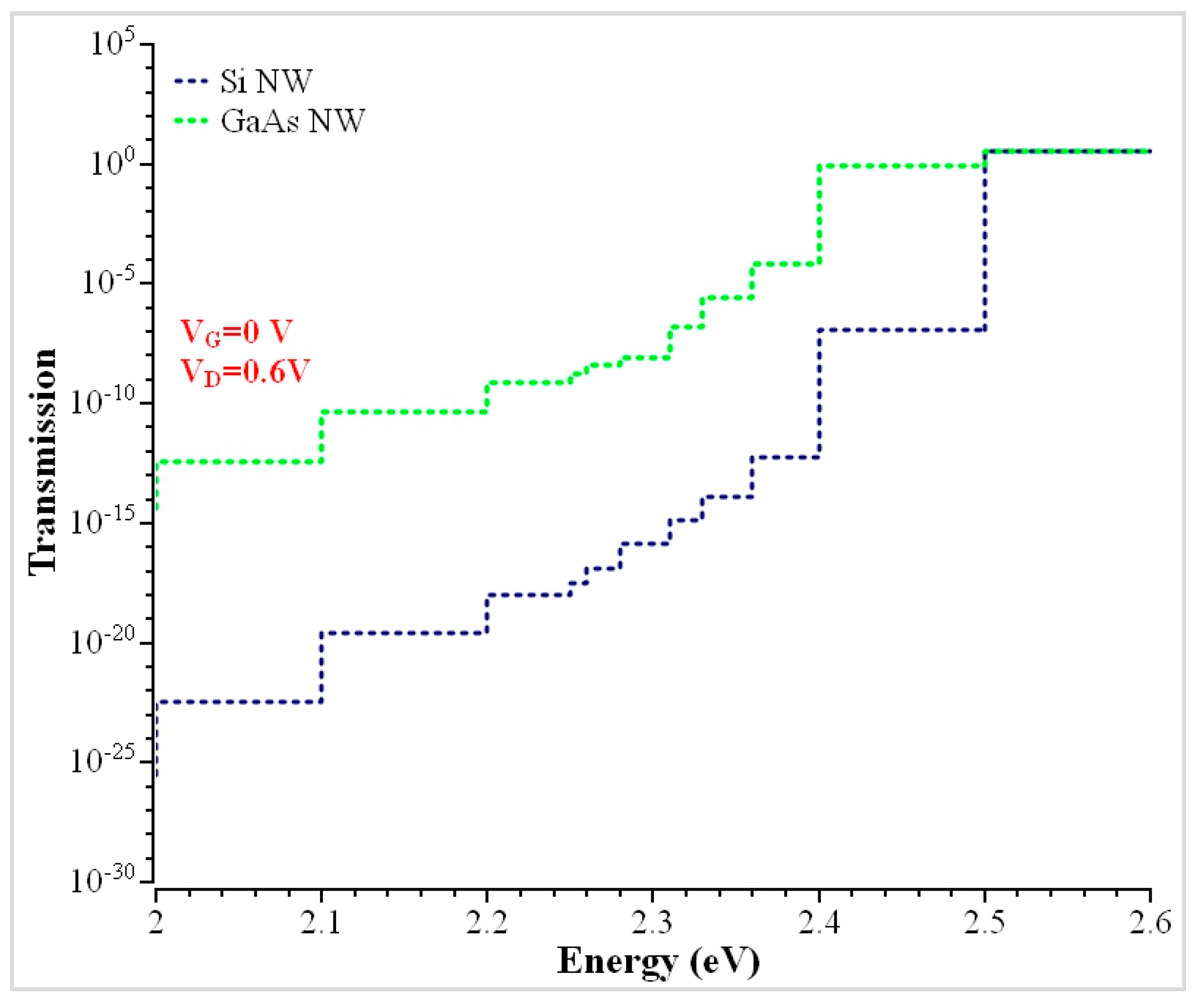
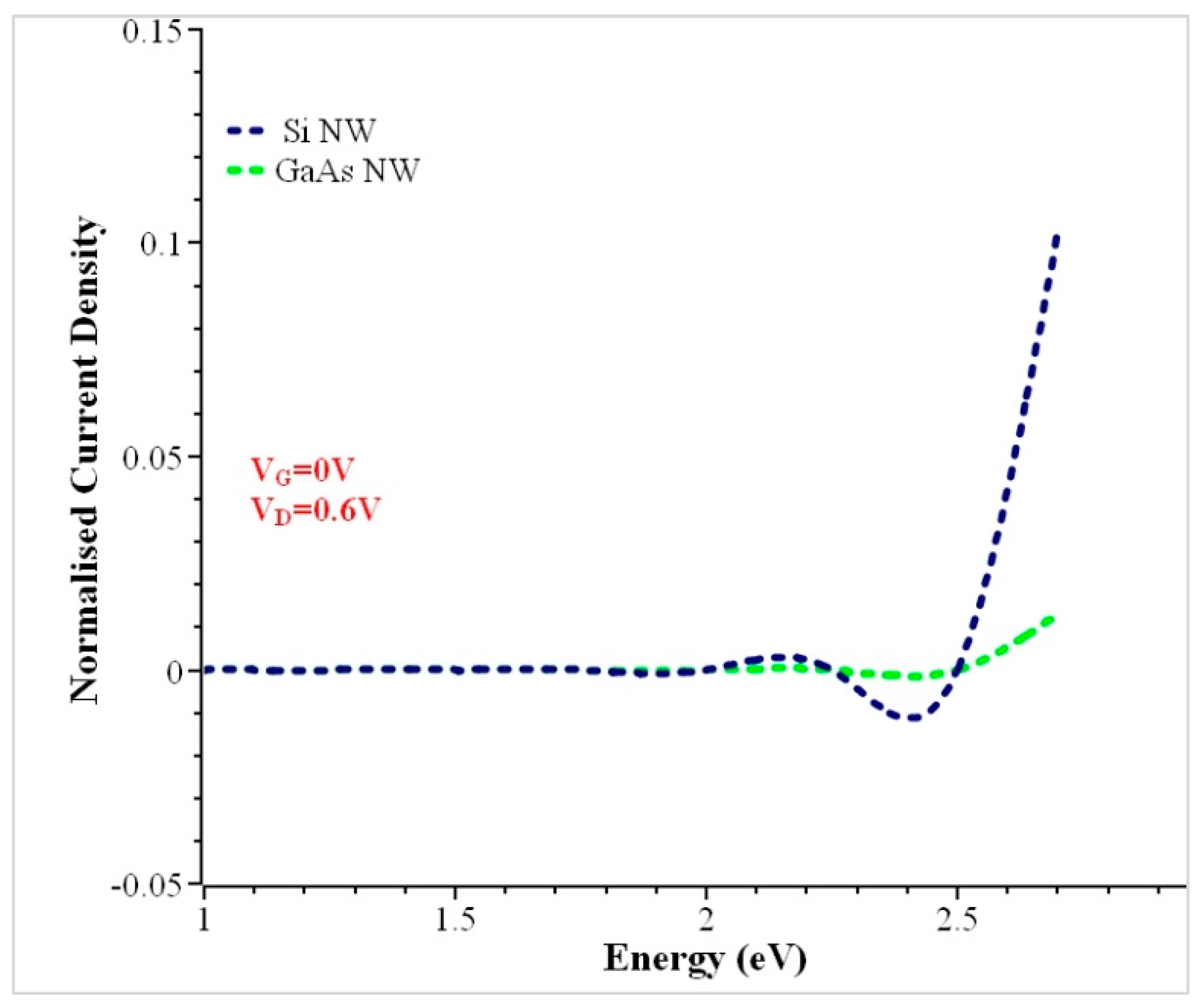
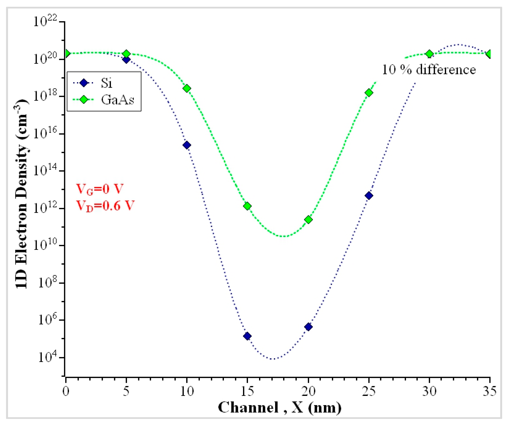
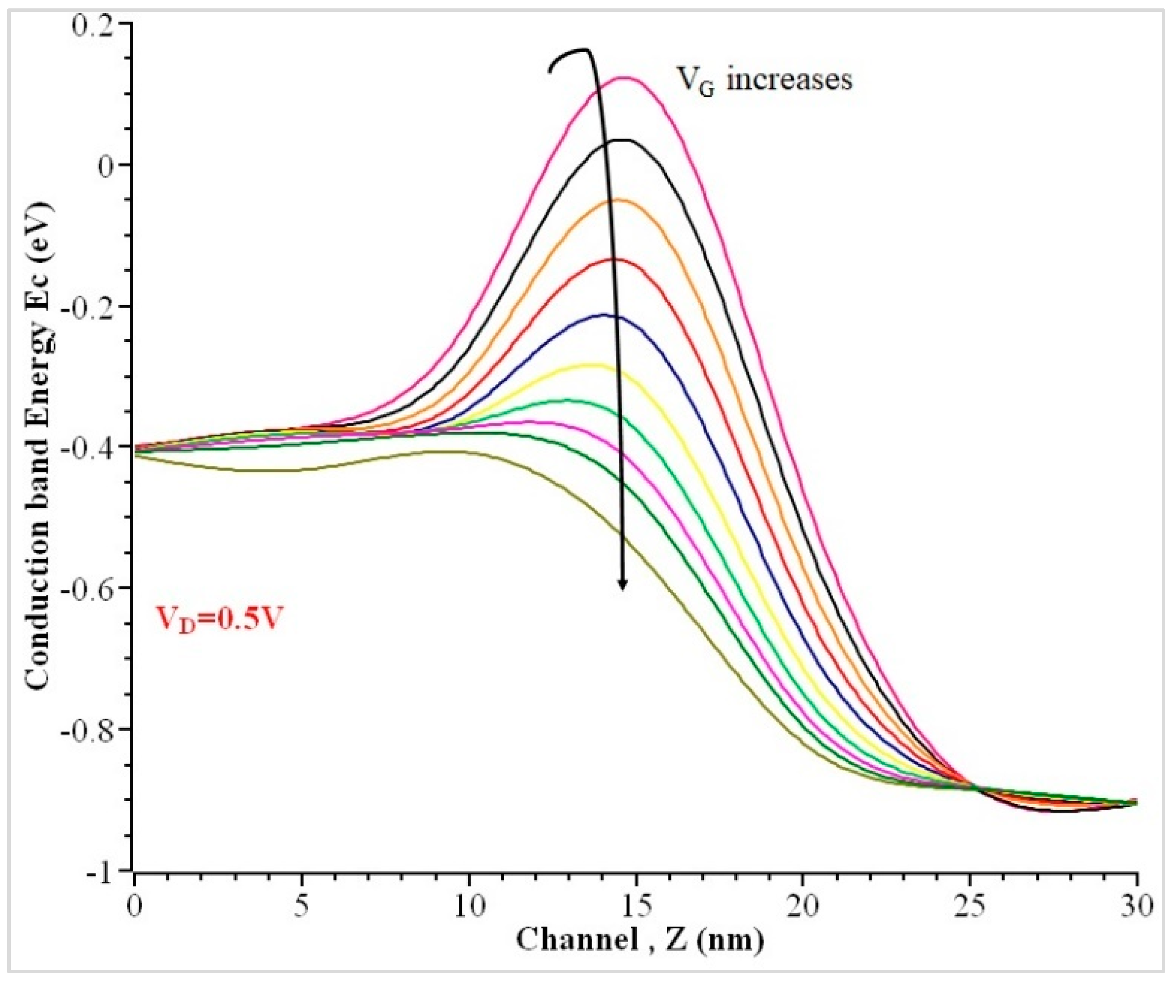
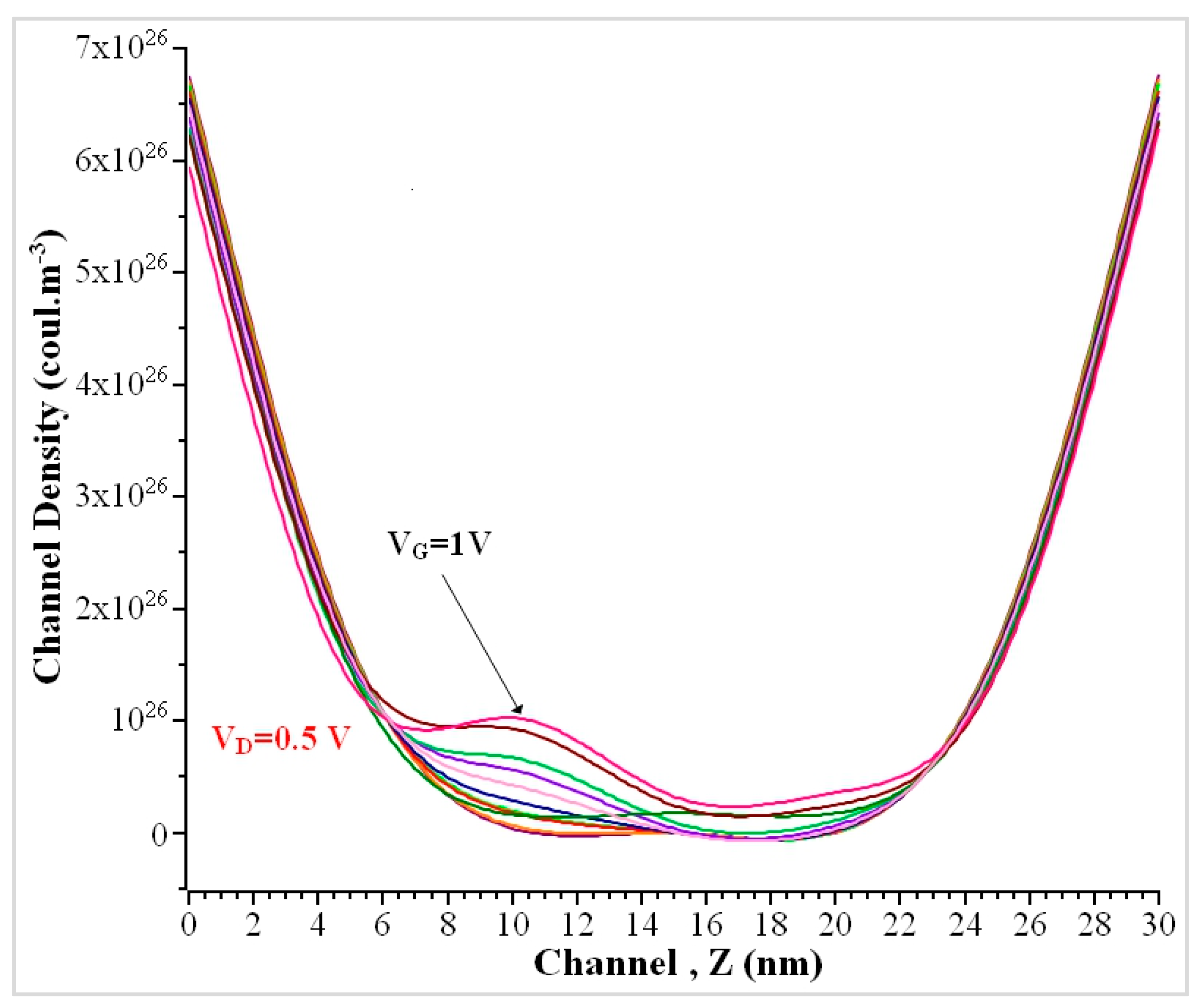
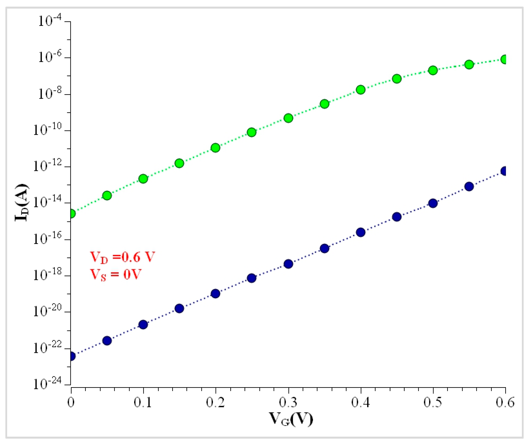
5. Analysis of the GaAs-Based Nanowire
6. Conclusions and Future Recommendations
Author Contributions
Funding
Data Availability Statement
Conflicts of Interest
References
- Colinge, J.P. FinFETs, and Other Multi-Gate Transistors; Springer US: New York, NY, USA, 2008. [Google Scholar]
- Goldberger, J.; Hochbaum, A.I.; Fan, R.; Yang, P. Silicon Vertically Integrated Nanowire Field Effect Transistors. Nano Lett. 2006, 6, 973–977. [Google Scholar]
- Natori, K. Ballistic/quasi-ballistic transport in nanoscale transistor. Appl. Surf. Sci. 2008, 254, 6194–6198. [Google Scholar] [CrossRef]
- Numata, T.; Uno, S.; Hattori, J.; Milnikov, G.; Kamakura, Y.; Mori, N.; Nakazato, K. A Self-Consistent Compact Model of Ballistic Nanowire MOSFET with Rectangular Cross Section. IEEE Trans. Electron Devices 2013, 60, 856–862. [Google Scholar] [CrossRef]
- Batakala, J.; Dhar, R.S. Effect of channel material on the performance parameters of GAA MOSFET. J. Nano Electron. Phys. 2022, 14, 02003. [Google Scholar] [CrossRef]
- Hosseini, R.; Fathipour, M.; Faez, R. A comparative study of NEGF and DDMS models in the GAA silicon nanowire transistor. Int. J. Electron. 2012, 99, 1299–1307. [Google Scholar] [CrossRef]
- Wang, J.; Polizzi, E.; Lundstrom, M. A Three-dimensional Quantum Simulation of Silicon Nanowire Transistors with the Effective-Mass Approximation. J. Appl. Phys. 2004, 96, 2192–2203. [Google Scholar] [CrossRef]
- Samuel, A.; Arumugam, N.; Shenbagavalli, A. Drain current characteristics of silicon nanowire field effect transistor. J. Microelectron. 2016, 2, 284–287. [Google Scholar] [CrossRef]
- Coquand, R.; Barraud, S.; Cass, M.; Leroux, P.; Vizioz, C.; Comboroure, C.; Perreau, P.; Ernst, E.; Samson, M.-P.; Maffini-Alvaro, V.; et al. Scaling of high-/metal-gate TriGate SOI nanowire transistors down to 10 nm width. Solid-State Electron. 2013, 88, 32–36. [Google Scholar] [CrossRef]
- Ramayya, E.B.; Vasileska, D.; Goodnick, S.M.; Knezevic, I. Electron transport in silicon nanowires: The role of acoustic phonon confinement and surface roughness scattering. J. Appl. Phys. 2008, 104, 063711. [Google Scholar] [CrossRef]
- Cresti, A.; Pala, M.G.; Poli, S.; Mouis, M.; Ghibaudo, G. A Comparative Study of Surface-Roughness-Induced Variability in Silicon Nanowire and Double-Gate FETs. IEEE Trans. Electron Devices 2011, 58, 2274–2281. [Google Scholar] [CrossRef]
- Jin, S.; Tang, T.; Fischetti, M.V. Anatomy of Carrier Backscattering in Silicon Nanowire Transistors. In Proceedings of the 2009 13th International Workshop on Computational Electronics, Beijing, China, 27–29 May 2009. [Google Scholar] [CrossRef]
- Dargar, S.K.; Srivastava, V.M. Performance analysis of High-k dielectric-based silicon nanowire gate-all-around tunneling FET. Int. J. Electr. Electron. Eng. Telecommun. 2019, 8, 340–345. [Google Scholar] [CrossRef]
- Srivastava, V.M.; Singh, G. MOSFET Technologies for Double-Pole Four-Throw Radio-Frequency Switch; Analog Circuits and Signal Processing; Springer International Publishing: Cham, Switzerland, 2014. [Google Scholar] [CrossRef]
- Martinez, A.; Seoane, N.; Brown, A.R.; Barker, J.R.; Asenov, A. 3-D Non-equilibrium Green’s Function Simulation of Nonperturbative Scattering from Discrete Dopants in the Source and Drain of a Silicon Nanowire Transistor. IEEE Trans. Nanotechnol. 2009, 8, 603–610. [Google Scholar] [CrossRef]
- Dubrovskii, V.G.; Hijazi, H.; Isik Goktas, N.; LaPierre, R.R. Be, Te and Si Doping of GaAs Nanowires: Theory and Experiment. J. Phys. Chem. C 2020, 124, 17299–17307. [Google Scholar] [CrossRef]
- Asenov, A.; Wang, Y.; Cheng, B.; Wang, X.; Asenov, P.; Al-Ameri, T.; Georgiev, V.P. Nanowire transistor solutions for 5 nm and beyond. In Proceedings of the 2016 17th International Symposium on Quality Electronic Design (ISQED), Santa Clara, CA, USA, 15–16 March 2016. [Google Scholar] [CrossRef]
- Svizhenko, A.; Anantram, M.P.; Govindan, T.R.; Biegel, B.; Venugopal, R. Two-dimensional quantum mechanical modeling of nanotransistors. J. Appl. Phys. 2002, 91, 2343–2354. [Google Scholar] [CrossRef]
- Luisier, M.; Schenk, A.; Fichtner, W. Quantum transport in two- and three-dimensional nanoscale transistors: Coupled mode effects in the non-equilibrium Green’s function formalism. J. Appl. Phys. 2006, 100, 043713. [Google Scholar] [CrossRef]
- Luisier, M.; Schenk, A.; Fichtner, W.; Klimeck, G. Atomistic simulation of nanowires in the sp3d5s* tight-binding formalism: From boundary conditions to strain calculations. Phys. Rev. B 2006, 74, 205323. [Google Scholar] [CrossRef]
- Luisier, M.; Schenk, A.; Fichtner, W.; Klimeck, G. Transport calculation of Semiconductor Nanowires Coupled to Quantum Well Reservoirs. J. Comput. Electron. 2006, 6, 199–202. [Google Scholar] [CrossRef]
- Gueorguiev, G.K.; Stafström, S.; Hultman, L. Nano-wire formation by self-assembly of silicon–metal cage-like molecules. Chem. Phys. Lett. 2008, 458, 170–174. [Google Scholar] [CrossRef]
- Kakanakova-Georgieva, A.; Ivanov, I.G.; Suwannaharn, N.; Hsu, C.-W.; Cora, I.; Pécz, B.; Gueorguiev, G.K. MOCVD of AlN on epitaxial graphene at extreme temperatures. CrystEngComm 2020, 23, 385–390. [Google Scholar] [CrossRef]
- Kumarasinghe, C.; Bowler, D.R. DFT study of undoped and As-doped Si nanowires approaching the bulk limit. J. Phys. Condens. Matter 2019, 32, 035304. [Google Scholar] [CrossRef]
- García-Cristóbal, A.; Molina-Sánchez, A. Tight-Binding Simulations of Nanowires. In Encyclopedia of Nanotechnology; Springer: Dordrecht, The Netherlands, 2015; pp. 1–12. [Google Scholar] [CrossRef]
- Morioka, N.; Yoshioka, H.; Suda, J.; Kimoto, T. Quantum-confinement effect on holes in silicon nanowires: Relationship between wave function and band structure. J. Appl. Phys. 2011, 109, 064318. [Google Scholar] [CrossRef]
- Paramasivam, P.; Gowthaman, N.; Srivastava, V.M. Design and analysis of InP/InAs/AlGaAs based Cylindrical Surrounding Double-Gate (CSDG) MOSFETs with La2O3 for 5-nm technology. IEEE Access 2021, 9, 159566–159576. [Google Scholar] [CrossRef]
- Gowthaman, N.; Srivastava, V.M. Mathematical modeling of drain current estimation in a CSDG MOSFET, based on La2O3 oxide layer with fabrication—A nanomaterial approach. Nanomaterials 2022, 12, 3374. [Google Scholar] [CrossRef]
- Neophytou, N.; Kosina, H. Hole mobility increase in ultra-narrow si channels under strong (110) surface confinement. Appl. Phys. Lett. 2011, 99, 092110. [Google Scholar] [CrossRef]
- Alam, K.; Sajjad, R.N. Electronic Properties and Orientation-Dependent Performance of InAs Nanowire Transistors. IEEE Trans. Electron Devices 2010, 57, 2880–2885. [Google Scholar] [CrossRef]
- Horiguchi, S. Validity of effective mass theory for energy levels in Si quantum wires. Phys. B Condens. Matter 1996, 227, 336–338. [Google Scholar] [CrossRef]
- Datta, S. Nanoscale device modeling: The Greens function method. Superlatt. Microstruct. 2000, 28, 253–278. [Google Scholar] [CrossRef]
- Ren, Z.; Venugopal, R.; Goasguen, S.; Datta, S.; Lundstrom, M.S. nanoMOS 2.5: A two-dimensional simulator for quantum transport in double-gate MOSFETs. IEEE Trans. Electron Devices 2003, 50, 1914–1925. [Google Scholar] [CrossRef]
- Martinez, A.; Barker, J.R. Quantum Transport in a Silicon Nanowire FET Transistor: Hot Electrons and Local Power Dissipation. Materials 2020, 13, 3326. [Google Scholar] [CrossRef]
- Abramo, A.; Cardin, A.; Selmi, L.; Sangiorgi, E. Two-dimensional quantum mechanical simulation of charge distribution in silicon MOSFETs. IEEE Trans. Electron Dev. 2000, 27, 1858–1863. [Google Scholar] [CrossRef]
- Seoane, N.; Martinez, A.; Brown, A.R.; Asenov, A. Study of surface roughness in extremely small Si nanowire MOSFETs using fully-3D NEGFs. In Proceedings of the 2009 Spanish Conference on Electron Devices, Santiago de Compostela, Spain, 11–13 February 2009. [Google Scholar] [CrossRef]
- Al Mamun Mazumdar, A.; Hosen, K.; Islam, M.S.; Park, J. Numerical investigations of nanowire gate-all-around negative capacitance GaAs/InN tunnel FET. Digit. Object Identifier 2022, 10, 30323–30334. [Google Scholar] [CrossRef]
- Montazeri, M.; Fickenscher, M.; Smith, L.M.; Jackson, H.E.; Yarrison-Rice, J.; Kang, J.H.; Gao, Q.; Tan, H.H.; Jagadish, C.; Guo, Y.; et al. Direct Measure of Strain and Electronic Structure in GaAs/GaP Core−Shell Nanowires. Nano Lett. 2010, 10, 880–886. [Google Scholar] [CrossRef] [PubMed]
- Ren, Z.; Lundstrom, M. Simulation of nanoscale MOSFETs: A scattering theory interpretation. Superlattices Microstruct. 2000, 27, 177–189. [Google Scholar] [CrossRef]
- Naveh, Y.; Likharev, K.K. Shrinking limits of silicon MOSFETs: Numerical study of 10 nm scale devices. Superlattices Microstruct. 2000, 27, 111–123. [Google Scholar] [CrossRef]
- Cheng, H.; Yang, Z.; Zhang, C.; Xie, C.; Liu, T.; Wang, J.; Zhang, Z. A New Approach to Modeling Ultrashort Channel Ballistic Nanowire GAA MOSFETs. Nanomaterials 2022, 12, 3401. [Google Scholar] [CrossRef] [PubMed]
- Pikus, F.G.; Likharev, K.K. Nanoscale field-effect transistors: An ultimate size analysis. Appl. Phys. Lett. 1997, 71, 3661–3663. [Google Scholar] [CrossRef]
- Ren, Z.; Venugopal, R.; Datta, S.; Lundstrom, M.; Jovanovic, D.; Fossum, J. International Electron Devices Meeting, 2000, IEDM Technical Digest. In Proceedings of the International Electron Devices Meeting. IEDM Technical Digest, Washington, DC, USA, 10 December 1997; p. 715. [Google Scholar]
- Natori, K. Scaling limit of the MOS transistor—A ballistic MOSFET. IEICE Trans. Electron. 2001, 84, 1029–1036. [Google Scholar]
- Rahman, A.; Jing Guo Datta, S.; Lundstrom, M.S. Theory of ballistic nanotransistors. IEEE Trans. Electron Devices 2003, 50, 1853–1864. [Google Scholar] [CrossRef]
- Naveh, Y.; Likharev, K.K. Modeling of 10-nm-Scale ballistic MOSFETs. IEEE Electron Device Lett. 2000, 21, 242–244. [Google Scholar] [CrossRef]
- Ren, Z.; Venugopal, R.; Datta, S.; Lundstrom, M.S.; Jovanovic, D.; Fossum, J.G. The ballistic nanotransistor: A simulation study. In Proceedings of the International Electron Devices Meeting 2000. Technical Digest. IEDM (Cat. No.00CH37138), San Francisco, CA, USA, 10–13 December 2000; pp. 715–718. [Google Scholar]
- Ren, Z. Nanoscale MOSFETs: Physics, Simulation, and Design. Ph.D. Thesis, Purdue Univ., West Lafayette, IN, USA, 2001. [Google Scholar]
- Mech, B.C.; Kumar, J. Effect of high-k dielectric on the performance of Si, InAs, and CNT FET. Micro Nano Lett. 2017, 12, 624–629. [Google Scholar] [CrossRef]
- Ren, Z.; Venugopal, R.; Datta, S.; Lundstrom, M.S. Examination of design and manufacturing issues in a 10 nm double gate MOSFET using non-equilibrium green’s function simulation. In Proceedings of the International Electron Devices Meeting. Technical Digest (Cat. No.01CH37224), Washington, DC, USA, 2–5 December 2001; pp. 5.4.1–5.4.4. [Google Scholar]
- Khan, T.; Iztihad, H.M.; Sufian, A.; Alam MN, K.; Mollah, M.N.; Islam, M.R. Gate length scaling of Si nanowire FET: A NEGF study. In Proceedings of the 2015 International Conference on Electrical Engineering and Information Communication Technology (ICEEICT), Savar, Bangladesh, 21–23 May 2015. [Google Scholar] [CrossRef]
- Gowthaman, N.; Srivastava, V.M. Mathematical modeling of electron density arrangement in CSDG MOSFET: A nano-material approach. J. Mater. Sci. 2022, 57, 8381–8392. [Google Scholar] [CrossRef]
- Moorthy, V.M.; Srivastava, V.M. Device modeling and optimization of nanomaterial-based planar heterojunction solar cell (by varying the device dimensions and material parameters). Nanomaterials 2022, 12, 3031. [Google Scholar] [CrossRef] [PubMed]
- Hiblot, G.; Rafhay, Q.; Boeuf, F.; Ghibaudo, G. Compact modeling of subthreshold swing in the double gate and nanowire MOSFETs, for Si and GaAs channel materials. Solid-State Electron. 2015, 111, 188–195. [Google Scholar] [CrossRef]
- Al-Ameri, T.; Wang, Y.; Georgiev, V.P.; Adamu-Lema, F.; Wang, X.; Asenov, A. Correlation between gate length, geometry, and electrostatically driven performance in ultra-scaled silicon nanowire transistors. In Proceedings of the 2015 IEEE Nanotechnology Materials and Devices Conference (NMDC), Anchorage, AK, USA, 13–16 September 2015. [Google Scholar] [CrossRef]
- Zhao, D.-H.; Tian, Z.-L.; Liu, H.; Gu, Z.-H.; Zhu, H.; Chen, L.; Zhang, D.W. Realizing Omega-Shaped Gate MoS2 Field-Effect Transistor Based on SiO2/MoS2 Core-Shell Heterostructure. ACS Appl. Mater. Interfaces 2020, 12, 14308–14314. [Google Scholar] [CrossRef]
- Natori, K. Ballistic metal-oxide-semiconductor field effect transistor. J. Appl. Phys. 1994, 76, 4879–4890. [Google Scholar] [CrossRef]


| Device Parameters | Proposed Nanowire |
|---|---|
| Tox (upper) nm | 1 |
| Tox(lower) nm | 1 |
| Channel Length (Lch) | 15 nm |
| Channel Width (Wch) | 2.5 nm |
| Channel Height (Hch) | 2.5 nm |
| Source Length (LS) | 10 nm |
| Drain length (LD) | 10 nm |
| S/D n + Donor doping (cm−3) | 2 × 10²⁰ |
| n channel doping (cm−3) | 1 × 10²⁰ |
| Shape | Rectangular |
| Transport | 100 |
| Confinement and Y direction | 010 |
| Gate Variant | No. of Gates ñ | Natural Length λn |
|---|---|---|
| Double Gate | 2 | 1.149 |
| GAA | 4 | 0.8129 |
| Omega Gate | 3.4 | 0.8817 |
| Pi Gate | 3.14 | 0.9175 |
| Top Gate | 1 | 1.625 |
| Tri-gate | 3 | 0.939 |
| Parameter | Si NW | GaAs NW |
|---|---|---|
| IDmax(A) | 6.08 × 10⁻⁸ | 8.20 × 10⁻⁸ |
| Transmission | 2.889 | 3.576 |
| Normalized Current Density | 1 | 1.06 × 10⁻⁶ |
| Electron Density, N1D(#/cm3) | 1.76 × 10²⁰ | 1.98 × 10²⁰ |
| ION (A) | 5.6 × 10⁻¹³ | 8.21 × 10⁻⁷ |
| IOFF (A) | 3.75 × 10⁻²³ | 2.62 × 10⁻¹⁵ |
| ION/IOFF | 1.49 × 10¹⁰ | 3.13 × 10⁸ |
| Subthreshold Slope SS (mV/decade) at VG = 0.1 V to 0.6 V | 8 mV to 107 mV | 8 mV to 99 mV |
| Parameter | DG | GAA | OMEGA | PI | TOP | TRI |
|---|---|---|---|---|---|---|
| ION (A) | 4.04 × 10⁻⁵ | 4.09 × 10⁻⁵ | 4.04 × 10⁻⁵ | 3.46 × 10⁻⁵ | 1.99 × 10⁻⁵ | 3.38 × 10⁻⁷ |
| IOFF (A) | 4.35 × 10⁻¹⁴ | 3.84 × 10⁻¹⁴ | 4.35 × 10⁻¹⁴ | 3.62 × 10⁻¹³ | 5.03 × 10⁻⁸ | 5.64 × 10⁻¹³ |
| ION/IOFF | 0.92 × 10⁹ | 1.06 × 10⁹ | 0.92 × 10⁹ | 0.95 × 10⁸ | 0.95 × 10³ | 0.6 × 10⁶ |
| Conduction band Ec in eV at 15 nm | −0.310 | −0.309 | −0.310 | −0.330 | −0.424 | −0.334 |
| Charge density ρ (Coul.m−3) at 15 nm | 6.42 × 10²³ | 6.24 × 10²³ | 6.42 × 10²³ | 1.01 × 1024 | 4.6 × 1024 | 1.01 × 1024 |
| Normalized current density | 1.03 × 1029 | 1.08 × 1029 | 1.03 × 1029 | 1.06 × 1029 | 1.07 × 1029 | 1.08 × 1029 |
| Subthreshold slope (mV) | 106 | 176 | 106 | 107 | 115 | 108 |
| No. of nodes | 9 | 9 | 10 | 10 | 10 | 9 |
| No. of iterations | 21 | 21 | 21 | 16 | 16 | 15 |
| NEGF simulation time in secs | 0.277 | 0.159 | 0.278 | 0.250 | 0.173 | 0.543 |
| Schrodinger simulation time in secs | 0.323 | 0.333 | 0.365 | 0.369 | 0.348 | 0.879 |
| Poisson simulation time in secs | 0.666 | 0.582 | 0.690 | 0.758 | 0.711 | 4.061 |
| Nanowire | Oxide (nm) | Lch (nm) | LG (nm) | VGS, VDS (V) | ION (A) | IOFF (A) | ION/IOFF |
|---|---|---|---|---|---|---|---|
| [4] | HFO2 | 5 | 20 | (0.6,0.6) | 4.5 × 10⁻⁵ | 0.1 × 10⁻⁶ | 4500 |
| [6] | SiO2 | 15 | 5 | (1,0.5) | 1 × 10⁻⁵ | 8.8 × 10⁻¹⁶ | 0.11 × 10¹¹ |
| [8] | SiO2 | 11 | 10 | (1,1) | 0.87 × 10⁻³ | 3.4 × 10⁻¹² | 0.25 × 10⁹ |
| [12] | SiO2 | 15 | 15 | (0.3,0.5) | 1.22 × 10⁻⁵ | 3 × 10⁻¹¹ | 0.40 × 10⁶ |
| [36] | SiO2 | 6 | 6 | (0.6, 0.001) | 1 × 10⁻⁶ | 1 × 10⁻¹³ | 1 × 10⁷ |
| [49] | La2O3 | 10 | 10 | (1,0.5) | 5.5 × 10³ | 0.84 × 10⁻⁸ | 6.54 × 10¹¹ |
| [51] | SiO2 | 5 | 6 | (0.6,0.6) | 9.8 × 10⁻⁷ | 3.4 × 10⁻¹³ | 2.88 × 10⁶ |
| This work | La2O3 | 15 | 2 | (1, 0.6) | 4.09 × 10⁻⁵ | 3.84 × 10⁻¹⁴ | 1.06 × 10⁹ |
| This work | La2O3 | 15 | 2 | (0.6, 0.6) | 2.11 × 10⁻⁶ | 3.84 × 10⁻¹⁴ | 0.55 × 10⁸ |
Disclaimer/Publisher’s Note: The statements, opinions and data contained in all publications are solely those of the individual author(s) and contributor(s) and not of MDPI and/or the editor(s). MDPI and/or the editor(s) disclaim responsibility for any injury to people or property resulting from any ideas, methods, instructions or products referred to in the content. |
© 2023 by the authors. Licensee MDPI, Basel, Switzerland. This article is an open access article distributed under the terms and conditions of the Creative Commons Attribution (CC BY) license (https://creativecommons.org/licenses/by/4.0/).
Share and Cite
Paramasivam, P.; Gowthaman, N.; Srivastava, V.M. Design and Analysis of Gallium Arsenide-Based Nanowire Using Coupled Non-Equilibrium Green Function for RF Hybrid Applications. Nanomaterials 2023, 13, 959. https://doi.org/10.3390/nano13060959
Paramasivam P, Gowthaman N, Srivastava VM. Design and Analysis of Gallium Arsenide-Based Nanowire Using Coupled Non-Equilibrium Green Function for RF Hybrid Applications. Nanomaterials. 2023; 13(6):959. https://doi.org/10.3390/nano13060959
Chicago/Turabian StyleParamasivam, Pattunnarajam, Naveenbalaji Gowthaman, and Viranjay M. Srivastava. 2023. "Design and Analysis of Gallium Arsenide-Based Nanowire Using Coupled Non-Equilibrium Green Function for RF Hybrid Applications" Nanomaterials 13, no. 6: 959. https://doi.org/10.3390/nano13060959
APA StyleParamasivam, P., Gowthaman, N., & Srivastava, V. M. (2023). Design and Analysis of Gallium Arsenide-Based Nanowire Using Coupled Non-Equilibrium Green Function for RF Hybrid Applications. Nanomaterials, 13(6), 959. https://doi.org/10.3390/nano13060959