
Domain Growth in Polycrystalline Graphene

Abstract
:1. Introduction
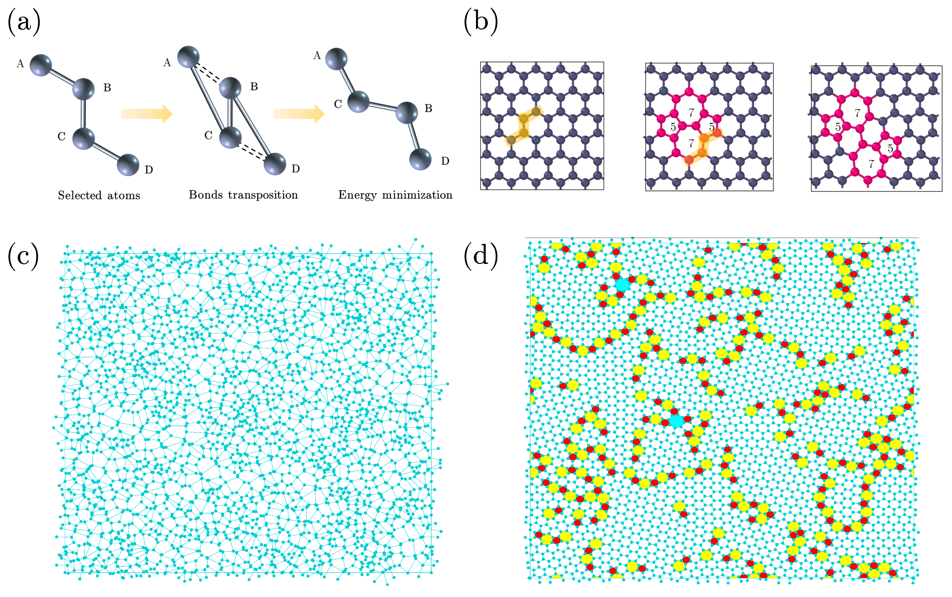
2. Model
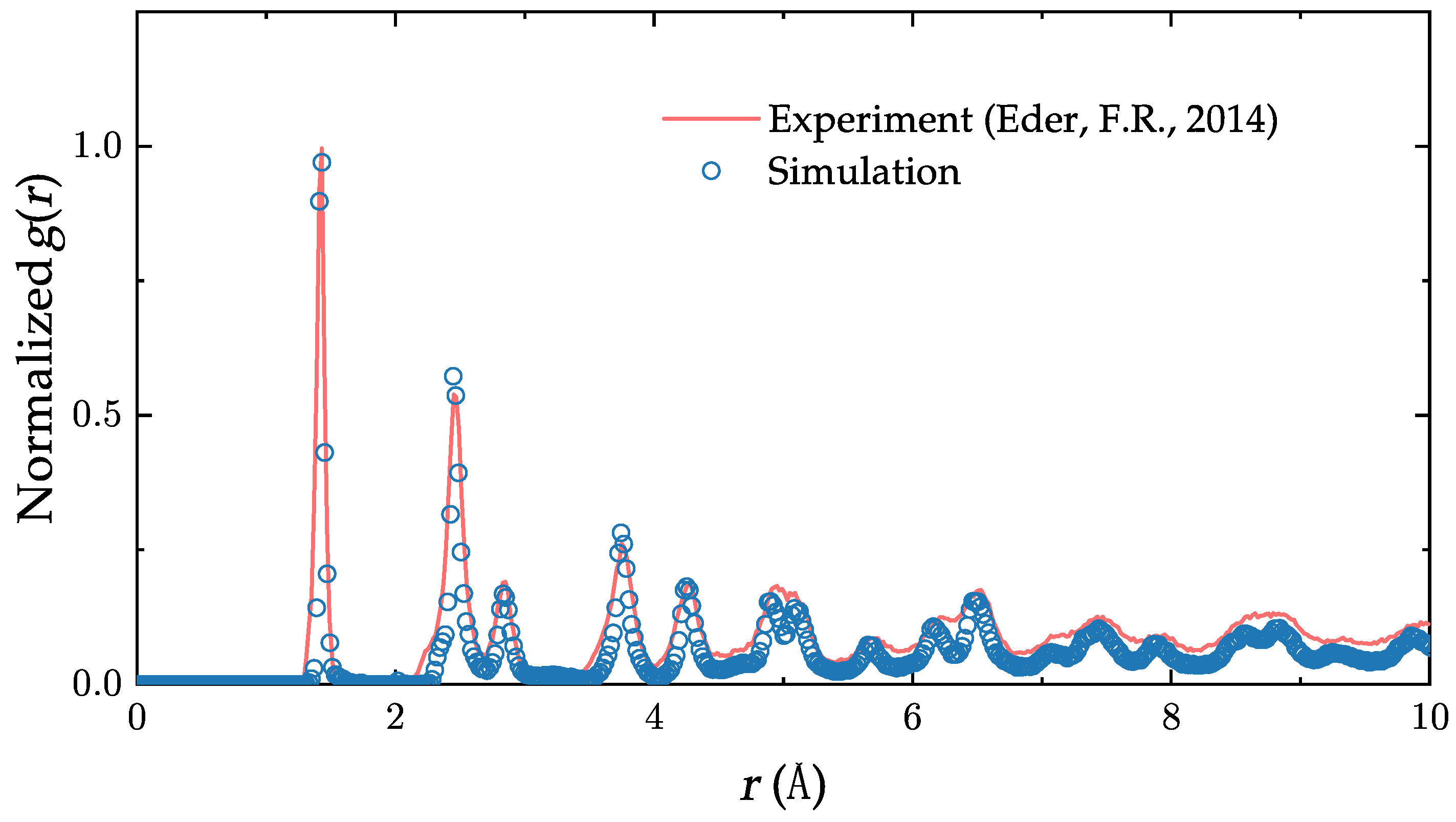
3. Model Validation
4. Results
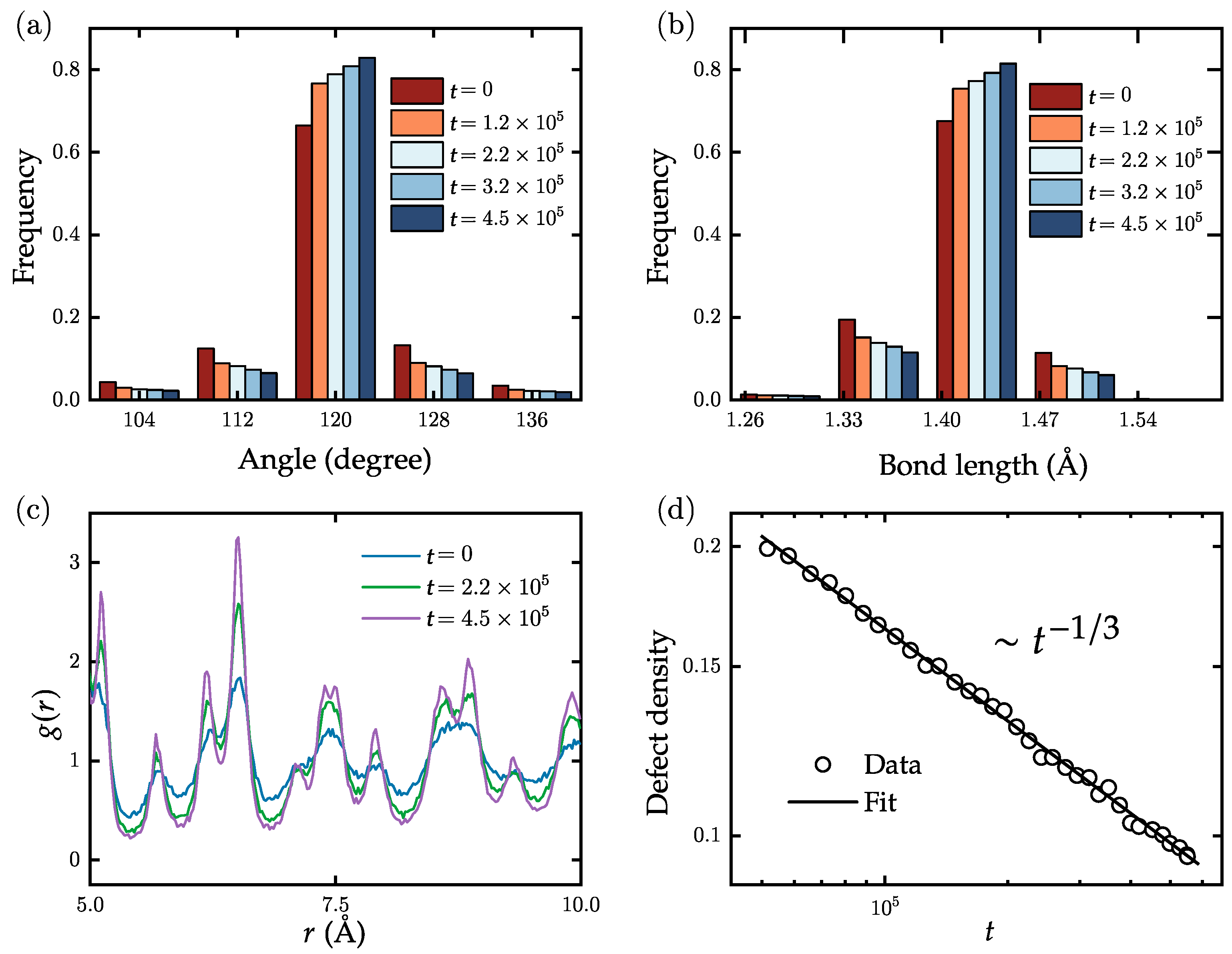
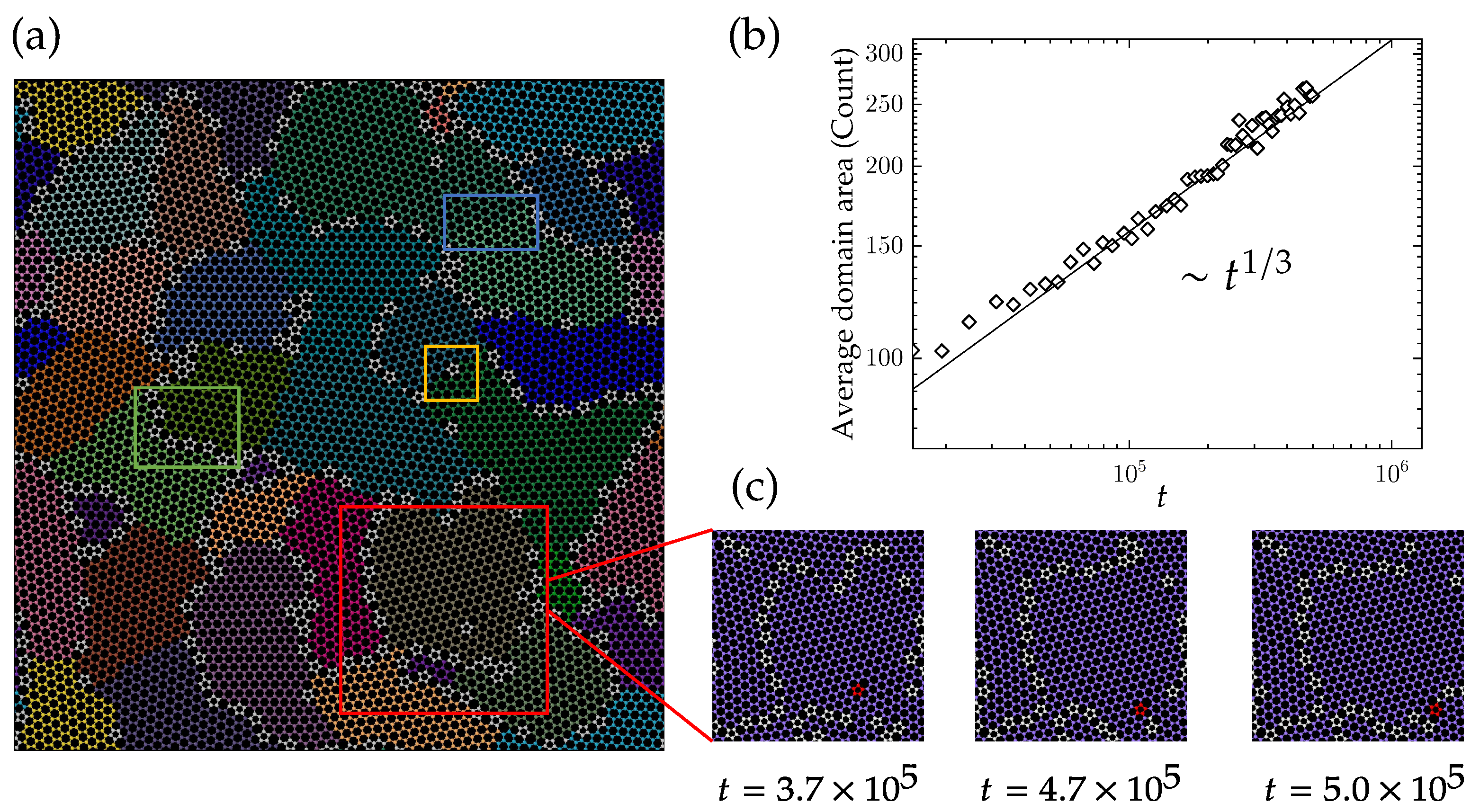
4.1. Domain Growth in Flat Polycrystalline Graphene
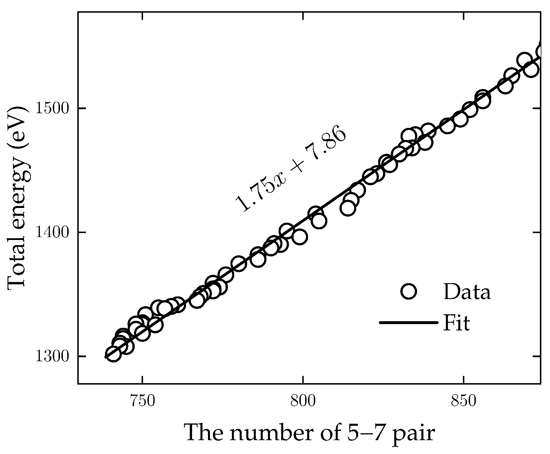
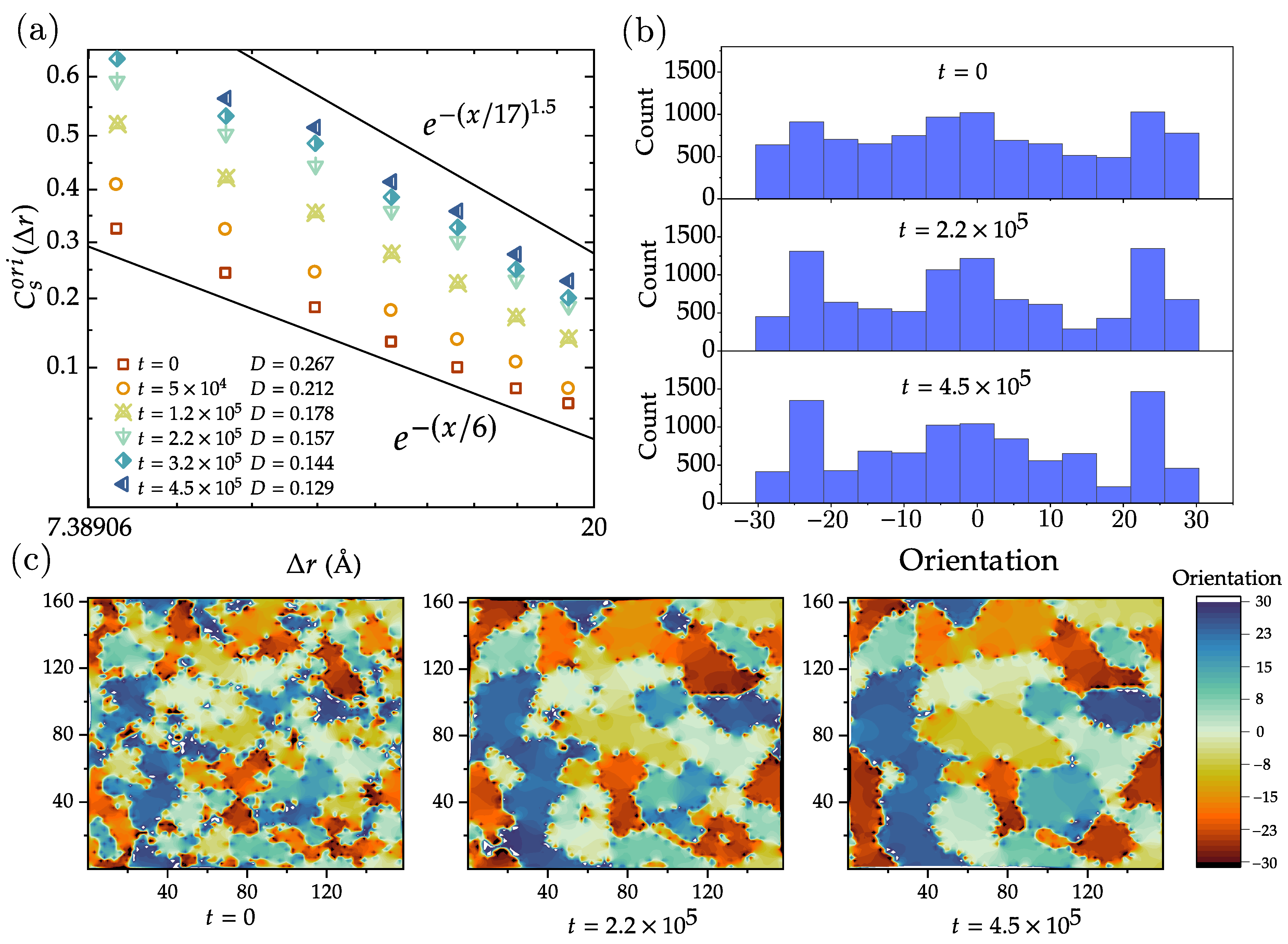
4.2. Dynamics of Crystal Phases
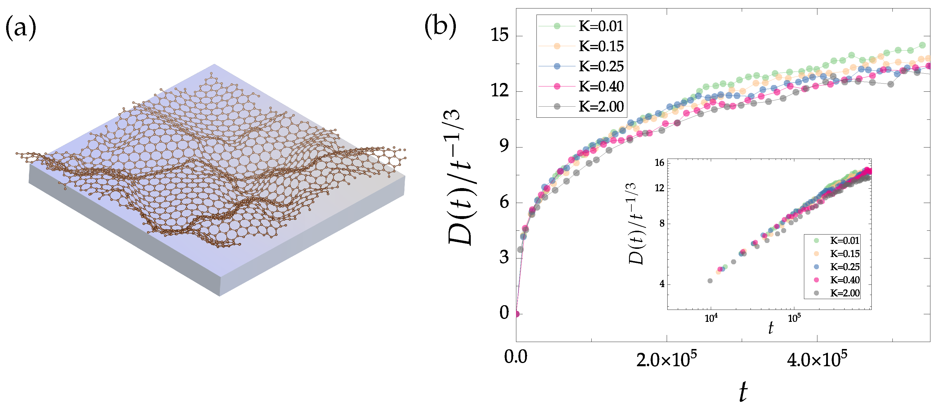
4.3. Domain Growth in Buckled Polycrystalline Graphene
5. Summary
Author Contributions
Funding
Data Availability Statement
Conflicts of Interest
References
- Song, N.; Gao, Z.; Li, X. Tailoring nanocomposite interfaces with graphene to achieve high strength and toughness. Sci. Adv. 2020, 6, eaba7016. [Google Scholar] [CrossRef]
- Zhang, P.; Ma, L.; Fan, F.; Zeng, Z.; Peng, C.; Loya, P.E.; Liu, Z.; Gong, Y.; Zhang, J.; Zhang, X.; et al. Fracture toughness of graphene. Nat. Commun. 2014, 5, 3782. [Google Scholar] [CrossRef]
- Shekhawat, A.; Ritchie, R.O. Toughness and strength of nanocrystalline graphene. Nat. Commun. 2016, 7, 10546. [Google Scholar] [CrossRef] [PubMed]
- Lee, C.; Wei, X.; Kysar, J.W.; Hone, J. Measurement of the elastic properties and intrinsic strength of monolayer graphene. Science 2008, 321, 385–388. [Google Scholar] [CrossRef] [PubMed]
- Zandiatashbar, A.; Lee, G.H.; An, S.J.; Lee, S.; Mathew, N.; Terrones, M.; Hayashi, T.; Picu, C.R.; Hone, J.; Koratkar, N. Effect of defects on the intrinsic strength and stiffness of graphene. Nat. Commun. 2014, 5, 3186. [Google Scholar] [CrossRef] [PubMed]
- Wang, M.; Yan, C.; Ma, L.; Hu, N.; Chen, M. Effect of defects on fracture strength of graphene sheets. Comput. Mater. Sci. 2012, 54, 236–239. [Google Scholar] [CrossRef]
- Balandin, A.A.; Ghosh, S.; Bao, W.; Calizo, I.; Teweldebrhan, D.; Miao, F.; Lau, C.N. Superior thermal conductivity of single-layer graphene. Nano Lett. 2008, 8, 902–907. [Google Scholar] [CrossRef] [PubMed]
- Chen, S.; Wu, Q.; Mishra, C.; Kang, J.; Zhang, H.; Cho, K.; Cai, W.; Balandin, A.A.; Ruoff, R.S. Thermal conductivity of isotopically modified graphene. Nat. Mater. 2012, 11, 203–207. [Google Scholar] [CrossRef] [PubMed]
- Kim, T.Y.; Park, C.H.; Marzari, N. The electronic thermal conductivity of graphene. Nano Lett. 2016, 16, 2439–2443. [Google Scholar] [CrossRef]
- Li, A.; Zhang, C.; Zhang, Y.F. Thermal conductivity of graphene-polymer composites: Mechanisms, properties, and applications. Polymers 2017, 9, 437. [Google Scholar] [CrossRef]
- Malekpour, H.; Chang, K.H.; Chen, J.C.; Lu, C.Y.; Nika, D.; Novoselov, K.; Balandin, A. Thermal conductivity of graphene laminate. Nano Lett. 2014, 14, 5155–5161. [Google Scholar] [CrossRef] [PubMed]
- Chen, H.; Müller, M.B.; Gilmore, K.J.; Wallace, G.G.; Li, D. Mechanically strong, electrically conductive, and biocompatible graphene paper. Adv. Mater. 2008, 20, 3557–3561. [Google Scholar] [CrossRef]
- Wang, Y.; Shi, Z.; Huang, Y.; Ma, Y.; Wang, C.; Chen, M.; Chen, Y. Supercapacitor devices based on graphene materials. J. Phys. Chem. C 2009, 113, 13103–13107. [Google Scholar] [CrossRef]
- Gwon, H.; Kim, H.S.; Lee, K.U.; Seo, D.H.; Park, Y.C.; Lee, Y.S.; Ahn, B.T.; Kang, K. Flexible energy storage devices based on graphene paper. Energy Environ. Sci. 2011, 4, 1277–1283. [Google Scholar] [CrossRef]
- Chen, P.Y.; Alù, A. Terahertz metamaterial devices based on graphene nanostructures. IEEE Trans. Terahertz Sci. Technol. 2013, 3, 748–756. [Google Scholar] [CrossRef]
- Zhang, F.; Zhang, T.; Yang, X.; Zhang, L.; Leng, K.; Huang, Y.; Chen, Y. A high-performance supercapacitor-battery hybrid energy storage device based on graphene-enhanced electrode materials with ultrahigh energy density. Energy Environ. Sci. 2013, 6, 1623–1632. [Google Scholar] [CrossRef]
- Zhang, Y.; Zhang, L.; Zhou, C. Review of chemical vapor deposition of graphene and related applications. Accounts Chem. Res. 2013, 46, 2329–2339. [Google Scholar] [CrossRef]
- Zhang, X.; Wang, L.; Xin, J.; Yakobson, B.I.; Ding, F. Role of hydrogen in graphene chemical vapor deposition growth on a copper surface. J. Am. Chem. Soc. 2014, 136, 3040–3047. [Google Scholar] [CrossRef]
- Liu, F.; Li, P.; An, H.; Peng, P.; McLean, B.; Ding, F. Achievements and challenges of graphene chemical vapor deposition growth. Adv. Funct. Mater. 2022, 32, 2203191. [Google Scholar] [CrossRef]
- Kidambi, P.R.; Ducati, C.; Dlubak, B.; Gardiner, D.; Weatherup, R.S.; Martin, M.B.; Seneor, P.; Coles, H.; Hofmann, S. The parameter space of graphene chemical vapor deposition on polycrystalline Cu. J. Phys. Chem. C 2012, 116, 22492–22501. [Google Scholar] [CrossRef]
- Mishra, N.; Boeckl, J.; Motta, N.; Iacopi, F. Graphene growth on silicon carbide: A review. Phys. Status Solidi (A) 2016, 213, 2277–2289. [Google Scholar] [CrossRef]
- Tetlow, H.; De Boer, J.P.; Ford, I.J.; Vvedensky, D.D.; Coraux, J.; Kantorovich, L. Growth of epitaxial graphene: Theory and experiment. Phys. Rep. 2014, 542, 195–295. [Google Scholar] [CrossRef]
- Xu, Y.; Cao, H.; Xue, Y.; Li, B.; Cai, W. Liquid-phase exfoliation of graphene: An overview on exfoliation media, techniques, and challenges. Nanomaterials 2018, 8, 942. [Google Scholar] [CrossRef] [PubMed]
- Ciesielski, A.; Samorì, P. Graphene via sonication assisted liquid-phase exfoliation. Chem. Soc. Rev. 2014, 43, 381–398. [Google Scholar] [CrossRef]
- Isacsson, A.; Cummings, A.W.; Colombo, L.; Colombo, L.; Kinaret, J.M.; Roche, S. Scaling properties of polycrystalline graphene: A review. 2D Mater. 2016, 4, 012002. [Google Scholar] [CrossRef]
- Cummings, A.W.; Duong, D.L.; Nguyen, V.L.; Van Tuan, D.; Kotakoski, J.; Barrios Vargas, J.E.; Lee, Y.H.; Roche, S. Charge transport in polycrystalline graphene: Challenges and opportunities. Adv. Mater. 2014, 26, 5079–5094. [Google Scholar] [CrossRef] [PubMed]
- Yazyev, O.V.; Chen, Y.P. Polycrystalline graphene and other two-dimensional materials. Nat. Nanotechnol. 2014, 9, 755–767. [Google Scholar] [CrossRef]
- Jain, S.K.; Barkema, G.T.; Mousseau, N.; Fang, C.M.; van Huis, M.A. Strong long-range relaxations of structural defects in graphene simulated using a new semiempirical potential. J. Phys. Chem. C 2015, 119, 9646–9655. [Google Scholar] [CrossRef]
- Barkema, G.T.; Mousseau, N. High-quality continuous random networks. Phys. Rev. B 2000, 62, 4985. [Google Scholar] [CrossRef]
- Wooten, F.; Winer, K.; Weaire, D. Computer generation of structural models of amorphous Si and Ge. Phys. Rev. Lett. 1985, 54, 1392. [Google Scholar] [CrossRef]
- D’Ambrosio, F.; Juričić, V.; Barkema, G.T. Discontinuous evolution of the structure of stretching polycrystalline graphene. Phys. Rev. B 2019, 100, 161402. [Google Scholar] [CrossRef]
- Guénolé, J.; Nöhring, W.G.; Vaid, A.; Houllé, F.; Xie, Z.; Prakash, A.; Bitzek, E. Assessment and optimization of the fast inertial relaxation engine (fire) for energy minimization in atomistic simulations and its implementation in lammps. Comput. Mater. Sci. 2020, 175, 109584. [Google Scholar] [CrossRef]
- Kirkwood, J.G. The skeletal modes of vibration of long chain molecules. J. Chem. Phys. 1939, 7, 506–509. [Google Scholar] [CrossRef]
- Liu, Z.; Panja, D.; Barkema, G.T. Structural dynamics of polycrystalline graphene. Phys. Rev. E 2022, 105, 044116. [Google Scholar] [CrossRef]
- Jain, S.K.; Juricic, V.; Barkema, G.T. Probing crystallinity of graphene samples via the vibrational density of states. J. Phys. Chem. Lett. 2015, 6, 3897–3902. [Google Scholar] [CrossRef] [PubMed]
- Ravinder, R.; Kumar, R.; Agarwal, M.; Krishnan, N.A. Evidence of a two-dimensional glass transition in graphene: Insights from molecular simulations. Sci. Rep. 2019, 9, 4517. [Google Scholar] [CrossRef]
- Eder, F.R.; Kotakoski, J.; Kaiser, U.; Meyer, J.C. A journey from order to disorder—Atom by atom transformation from graphene to a 2D carbon glass. Sci. Rep. 2014, 4, 4060. [Google Scholar] [CrossRef]
- Stukowski, A. Structure identification methods for atomistic simulations of crystalline materials. Model. Simul. Mater. Sci. Eng. 2012, 20, 045021. [Google Scholar] [CrossRef]
- Felix, I.M.; Pereira, L.F.C. Thermal conductivity of graphene-hBN superlattice ribbons. Sci. Rep. 2018, 8, 2737. [Google Scholar] [CrossRef]
- Ramos, P.M.; Herranz, M.; Foteinopoulou, K.; Karayiannis, N.C.; Laso, M. Identification of local structure in 2-d and 3-d atomic systems through crystallographic analysis. Crystals 2020, 10, 1008. [Google Scholar] [CrossRef]
- Han, Y.; Song, L.; Wang, B.; Sun, S.; Qian, Q.; Wang, Q. AtomicNet: A novel approach to identify the crystal structure of each simulated atom. Model. Simul. Mater. Sci. Eng. 2020, 28, 035005. [Google Scholar] [CrossRef]
- Larsen, P.M.; Schmidt, S.; Schiøtz, J. Robust structural identification via polyhedral template matching. Model. Simul. Mater. Sci. Eng. 2016, 24, 055007. [Google Scholar] [CrossRef]
- Bonald, T.; Charpentier, B.; Galland, A.; Hollocou, A. Hierarchical graph clustering using node pair sampling. arXiv 2018, arXiv:1806.01664. [Google Scholar]
- Newman, M.E.; Barkema, G.T. Monte Carlo Methods in Statistical Physics; Clarendon Press: Oxford, UK, 1999. [Google Scholar]
- Tison, Y.; Lagoute, J.; Repain, V.; Chacon, C.; Girard, Y.; Joucken, F.; Sporken, R.; Gargiulo, F.; Yazyev, O.V.; Rousset, S. Grain boundaries in graphene on SiC (0001) substrate. Nano Lett. 2014, 14, 6382–6386. [Google Scholar] [CrossRef]
Disclaimer/Publisher’s Note: The statements, opinions and data contained in all publications are solely those of the individual author(s) and contributor(s) and not of MDPI and/or the editor(s). MDPI and/or the editor(s) disclaim responsibility for any injury to people or property resulting from any ideas, methods, instructions or products referred to in the content. |
© 2023 by the authors. Licensee MDPI, Basel, Switzerland. This article is an open access article distributed under the terms and conditions of the Creative Commons Attribution (CC BY) license (https://creativecommons.org/licenses/by/4.0/).
Share and Cite
Liu, Z.; Panja, D.; Barkema, G.T. Domain Growth in Polycrystalline Graphene. Nanomaterials 2023, 13, 3127. https://doi.org/10.3390/nano13243127
Liu Z, Panja D, Barkema GT. Domain Growth in Polycrystalline Graphene. Nanomaterials. 2023; 13(24):3127. https://doi.org/10.3390/nano13243127
Chicago/Turabian StyleLiu, Zihua, Debabrata Panja, and Gerard T. Barkema. 2023. "Domain Growth in Polycrystalline Graphene" Nanomaterials 13, no. 24: 3127. https://doi.org/10.3390/nano13243127
APA StyleLiu, Z., Panja, D., & Barkema, G. T. (2023). Domain Growth in Polycrystalline Graphene. Nanomaterials, 13(24), 3127. https://doi.org/10.3390/nano13243127