Article

In Situ Sintering of CdSe/CdS Nanocrystals under Electron Beam Irradiation

1
College of Mechanical and Electrical Engineering, Nanjing Forestry University, Nanjing 210037, China
2
SEU-FEI Nano-Pico Center, Key Lab of MEMS of Ministry of Education, Southeast University, Nanjing 210096, China
3
College of Electronic and Optical Engineering & College of Flexible Electronics (Future Technology), Nanjing University of Posts and Telecommunications, Nanjing 210023, China
4
College of Electrical Engineering, Yanshan University, Qinhuangdao 066004, China
*
Author to whom correspondence should be addressed.
Nanomaterials 2023, 13(24), 3082; https://doi.org/10.3390/nano13243082
Submission received: 2 November 2023 / Revised: 29 November 2023 / Accepted: 1 December 2023 / Published: 5 December 2023
(This article belongs to the Special Issue Nanomanufacturing-Based Microelectromechanical Systems)

Abstract

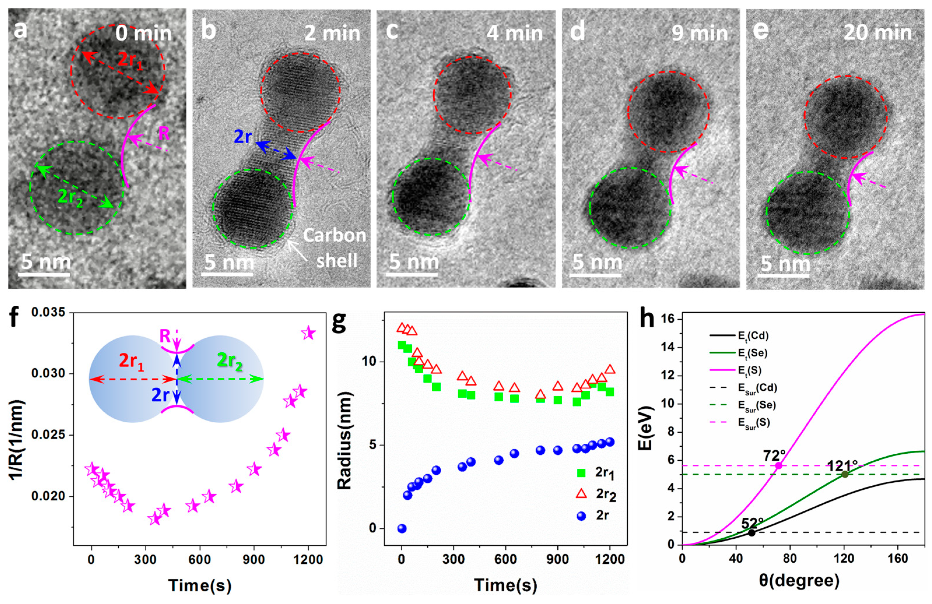
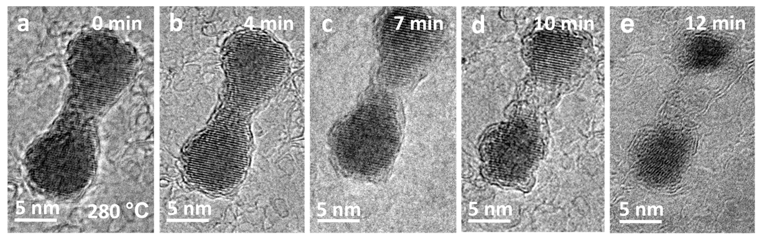
Colloidal semiconductor nanocrystals have attracted widespread attention due to their tremendous electrical and optical properties. Nanoparticles exhibit a strong tendency to aggregate and sinter in a short period of time during processing or use due to their large surface area-to-volume ratio, which may lead to significant changes in their required performance. Therefore, it is of great significance to conduct in-depth research on the sintering process and mechanism of nanoparticles to maintain their stability. Here, the sintering process of CdSe/CdS core/shell nanocrystals under continuous electron beam irradiation was studied using in situ transmission electron microscopy (TEM). In the early stages of sintering, CdSe/CdS nanocrystals approached each other at a distance of approximately 1–2 nm. As the exposure time to the electron beam increased, the movement of surface atoms on the nanocrystals led to contact between them. Subsequently, the atoms on the contact surfaces underwent rapid motion, resulting in the rapid formation of the neck between the particles. The neck formation between adjacent particles provides strong evidence of a sintering mechanism dominated by surface atom diffusion rather than Ostwald ripening. Further research in this area could lead to the development of improved methods to prevent sintering and enhance the stability of nanocrystals, ultimately contributing to the advancement of nanomaterial-based devices and materials with long-lasting performance.
Keywords: electron beam irradiation; CdSe/CdS nanocrystals; sintering; surface atom diffusion; transmission electron microscopy electron beam irradiation; CdSe/CdS nanocrystals; sintering; surface atom diffusion; transmission electron microscopy