Article

Capacitive NO2 Detection Using CVD Graphene-Based Device

1
Department of Physics and Photon Science, Gwangju Institute of Science and Technology, Gwangju 61005, Republic of Korea
2
Korea Institute of Energy Technology, KENTECH College, Naju 58330, Jeonnam, Republic of Korea
*
Author to whom correspondence should be addressed.
Nanomaterials 2023, 13(2), 243; https://doi.org/10.3390/nano13020243
Submission received: 5 December 2022 / Revised: 31 December 2022 / Accepted: 3 January 2023 / Published: 5 January 2023

Abstract

:
A graphene-based capacitive NO2 sensing device was developed by utilizing the quantum capacitance effect. We have used a graphene field-effect transistor (G-FET) device whose geometrical capacitance is enhanced by incorporating an aluminum back-gate electrode with a naturally oxidized aluminum surface as an insulating layer. When the graphene, the top-side of the device, is exposed to NO2, the quantum capacitance of graphene and, thus, the measured capacitance of the device, changed in accordance with NO2 concentrations ranging from 1–100 parts per million (ppm). The operational principle of the proposed system is also explained with the changes in gate voltage-dependent capacitance of the G-FET exposed to various concentrations of NO2. Further analyses regarding carrier density changes and potential variances under various concentrations of NO2 are also presented to strengthen the argument. The results demonstrate the feasibility of capacitive NO2 sensing using graphene and the operational principle of capacitive NO2 sensing.

1. Introduction

Since the discovery of graphene, a two-dimensional carbon atomic layer prepared by mechanical exfoliation of highly oriented pyrolytic graphite, it has garnered the attention of many researchers due to its unique electronic, optical, and mechanical properties [1,2,3,4,5,6,7]. One of the promising applications is its usage as a sensing material for chemicals, owing to its electrical properties, large surface-to-volume ratio, and chemical stability [8]. The sensing ability of graphene extends to detection of a wide range of chemicals, such as NO2, CO, SO2, H2S, etc. [8,9,10,11]. Furthermore, functionalized graphene, defective graphene, and doped graphene have been studied to improve the selectivity and sensitivity of graphene-based sensing devices [12,13,14,15,16]. Graphene-based gas sensing devices have great of potential for detecting dangerous gas species [17], such as nitrogen dioxide (NO2), one of the dangerous air pollutants that can affect human health even in low concentrations [18,19]. In this respect, graphene-based NO2 sensing applications have been extensively studied for decades. However, most of related research has been focused on measuring a change in resistance (or conductance) when chemicals are adsorbed on a graphene surface [20,21,22,23].
Although graphene-based capacitive sensing applications have been studied in recent years with various chemicals and gas/vapors [24,25,26,27], an extensive study on capacitive NO2 sensing has not yet been reported. The total capacitance (Ctotal) of a graphene-based capacitive sensing device consists of the series connection of geometrical capacitance (Cgeo) and quantum capacitance (CQ). The quantum capacitance effect is the main reason behind the changes in Ctotal upon the adsorption of chemical molecules on the graphene surface. However, due to the electrical characteristics of a system of capacitors, the system requires greater Cgeo compared to the minimum CQ (or at least equal to CQ), in order for Ctotal to be dominantly determined by CQ. This indicates that the sensitivity of the capacitive sensing device can be improved by enhancing the Cgeo [24,28,29]. Further analyses of quantum capacitance provide electronic properties of materials, such as the density of states, carrier density, and potential variance [28,30,31,32,33], which allows us to confirm the working principle of the proposed device.
In this work, we report capacitive NO2 sensing performance of an Al back-gated G-FET. Various gas molecules (NH3, H2O, CO, O2, NO2, etc.) can be adsorbed on graphene surfaces due to various reasons on graphene surfaces, resulting in changes in electronic response. The issue of functionalizing a graphene surface to increase the selectivity of a target molecule is a completely different issue yet to be resolved. However, we can still test the electrical responses of graphene-based devices by creating isolated environments to test the sensing procedure. Furthermore, the adsorbed gas molecules on graphene can be easily detached by thermal treatment or UV exposure, which allows us to recycle the prepared devices for the test under various conditions. To investigate the capacitive response of graphene for NO2, we restricted the test gases to a NO2/N2 mixture and adopted UV exposure for the recovery process. Water molecules in the air affect the quantum capacitance of graphene by adsorbing it onto graphene surfaces [25]. Oxygen molecules can also affect the quantum capacitance of graphene by adsorbing onto graphene surfaces. However, diluted NO2 in dry air was detected well using graphene-based devices by measuring its resistance [34]. In order to use the proposed device in daily life, response tests for NO2 diluted in ambient air as a function of humidity should be further studied.
We focus on capacitive NO2 sensing performance, and later, the electronic properties of graphene exposed to NO2 molecules will be discussed to strengthen our argument regarding the working principle of the device. Changes in the capacitance of the device were measured before and after the vacuum test chamber was filled with various concentrations of NO2 (1–100 ppm balanced with pure nitrogen gas). Furthermore, the electronic properties, such as residual carrier density and potential variance at different NO2 concentrations, were extracted from the gate voltage-dependent Ctotal. Our results demonstrate the feasibility of capacitive NO2 sensing and, thus, provide preliminary research for capacitive gas sensing using graphene.

2. Methods

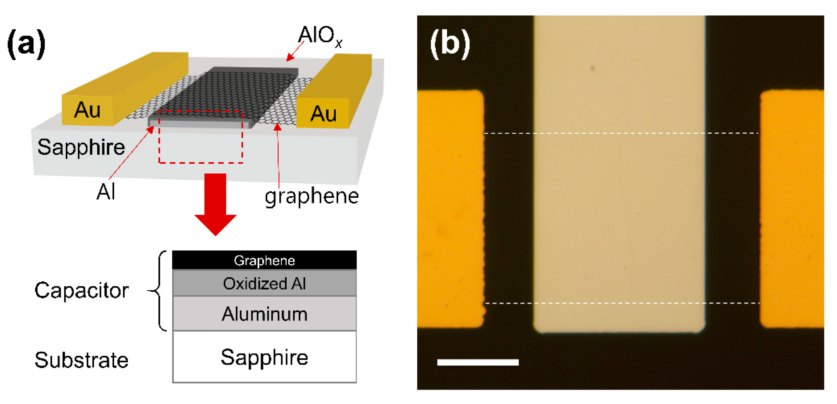
2.1. Device Fabrication

A capacitive NO2 sensing device was fabricated using CVD-grown graphene on Cu foil (LG electronics). Monolayer graphene was confirmed by Raman spectroscopy, as shown in Figure S1. At first, 15 nm of Al back-gate electrode was deposited on a sapphire substrate using photolithography and electron beam evaporation. Soon after the sample was removed from the evaporation chamber, oxidation took place, forming a few nanometers-thick layer of oxidized Al (AlOx) on the surface of the Al gate electrode. Later, this extra thin layer of AlOx would serve as a high-k insulating layer for the graphene-based capacitor with a relatively large geometric capacitance. Next, CVD graphene was transferred onto the sapphire substrate. The Cu foil with top-side graphene was spin-coated with poly(methyl methacrylate) (PMMA) (4% in anisole) and then baked on a hot plate at 120 °C for 10 min. The reverse side of the graphene (lacking PMMA) was etched using O2 reactive-ion etching (RIE). Afterwards, PMMA/graphene on the Cu foil was placed in ammonium persulfate solution (5 wt% in distilled water) for more than 3 h to remove the Cu foil. After finishing the Cu foil etching, the graphene/PMMA film was transferred to distilled water three times to rinse the residual chemicals beneath the graphene. Subsequently, the PMMA-supported graphene film was transferred to the target substrate. Then, the sample was dried in an oven at 60 °C for more than 5 min. The PMMA layer on the substrate was removed by soaking in acetone for more than an hour. The graphene channel was patterned using photolithography and O2 RIE. Finally, 40 nm of Au source and drain electrodes were formed on the graphene channel using photolithography and electron beam evaporation. A cross-sectional view and an optical microscopy image of the fabricated device are shown in Figure 1a,b, respectively. The active capacitive sensing area is graphene on the Al back-gate electrode, as marked with the red dashed line in Figure 1a.

2.2. Measurement Setup

Gas sensing measurements were carried out in a test chamber equipped with pure nitrogen (N2 99.999%) and 100 ppm NO2 (balanced with N2) gas, mass flow controllers (MFCs), a UV lamp (TUV 4W G4T5, Philips, Seoul, Republic of Korea), a measuring instrument (4200-SCS, Keithley, Cleveland, OH, USA), a mechanical pump, and a quartz window, as shown in Figure 2. To measure the NO2 sensing performance, various concentrations (1–100 ppm) of NO2 gas are introduced into the test chamber by varying the ratio of the flow rate of 100 ppm NO2 and pure N2 using MFCs at a total flow rate of 10 standard liters per minute (SLM). The gas sensing performance of the device under test (DUT) is monitored by the change in capacitance caused by gas molecule adsorption on the graphene surface. The UV lamp outside the chamber is used during the recovery process; the distance between the device under test and the UV lamp is approximately 7 cm. All electrical measurements were carried out using a Keithley 4200-SCS at room temperature.

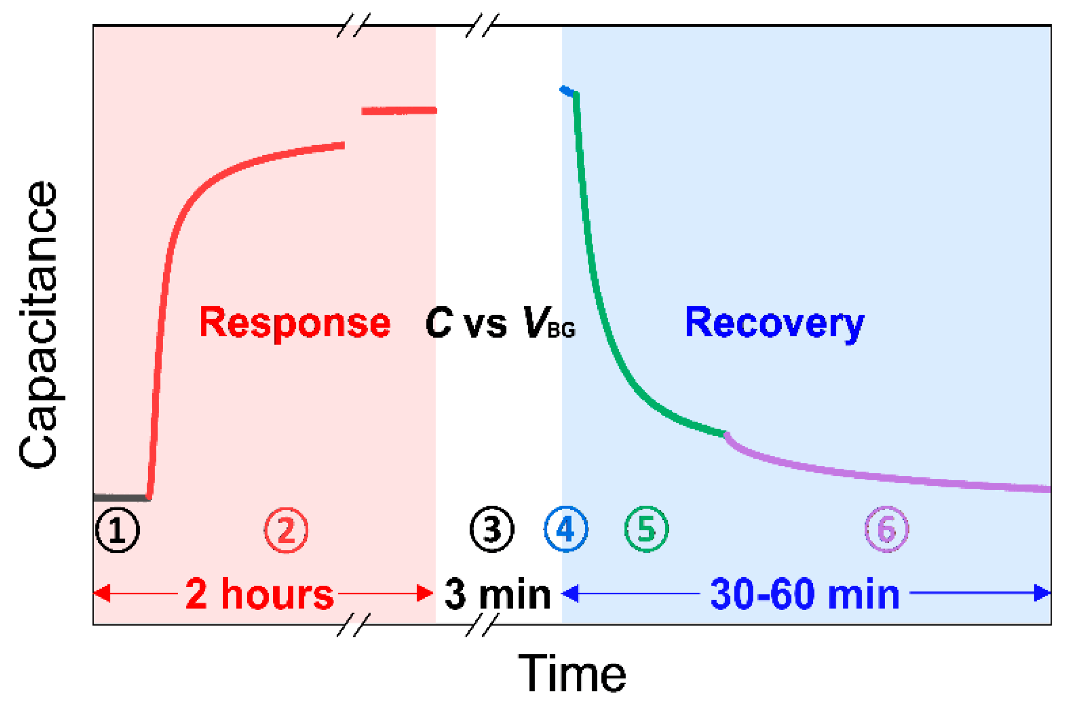
2.3. Measurement Flow

Before beginning the sensing measurements, the mechanical pump evacuates the chamber to its initialized state at a pressure of around 10−3 torr (the black line in Figure 3). While measuring capacitance in real-time under vacuum (stage ➀), the gas mixture of NO2/N2 with a target concentration is injected into the initialized test chamber until the pressure reaches atmospheric pressure (~760 torr). Then, all the valves are closed to isolate the chamber. The device is exposed to an NO2 environment for approximately 2 h to check capacitance saturation time (stage ➁). To characterize sensing performance, the response is calculated using the following equation:
Response = | C g C 0 C 0 | × 100 %
where Cg and C0 are the capacitance before and after the exposure to NO2, respectively [35]. Then, Ctotal is measured by sweeping the back-gate voltage, VBG from +2 V to −2 V, to analyze the electronic properties of graphene exposed to different concentrations of NO2 (stage ➂).
Thermal treatment and UV illumination can be used to detach adsorbates on graphene [8,22,34,36]. The UV illumination method was adopted for our recovery process because of its timely response compared to thermal treatment in our measurement setup. The UV light generates electron–hole pairs that detach the NO2 adsorbates via hole recombination, e.g., hole + NO2 → NO2 (gas), on graphene [22,37]. Though appropriate UV exposure in ambient air improves the recovery process, overexposure to UV light under ambient condition may generate ozone, causing damage to the carbon–carbon bonding in graphene and creating defects. However, UV irradiation on graphene in inert gas or vacuum does not significantly affect the defect sites [37,38]. Furthermore, the graphene sensors for NO2 have been known to exhibit excellent durability and reliability for the UV-assisted recovery process [22].
Thus, during the recovery process, the chamber is first evacuated by a mechanical pump to reduce the residual NO2 molecules and possible introduction of O2 in the chamber (stage ➃). While pumping, the UV light is turned on to detach the adsorbed gas molecules from the graphene surface (stage ➄) and then tuned off (stage ➅) until the capacitance of the device returns to the initial state (the capacitance before NO2 exposure). Then, the response, gate sweeping, and recovery processes are repeated with different concentrations of NO2.

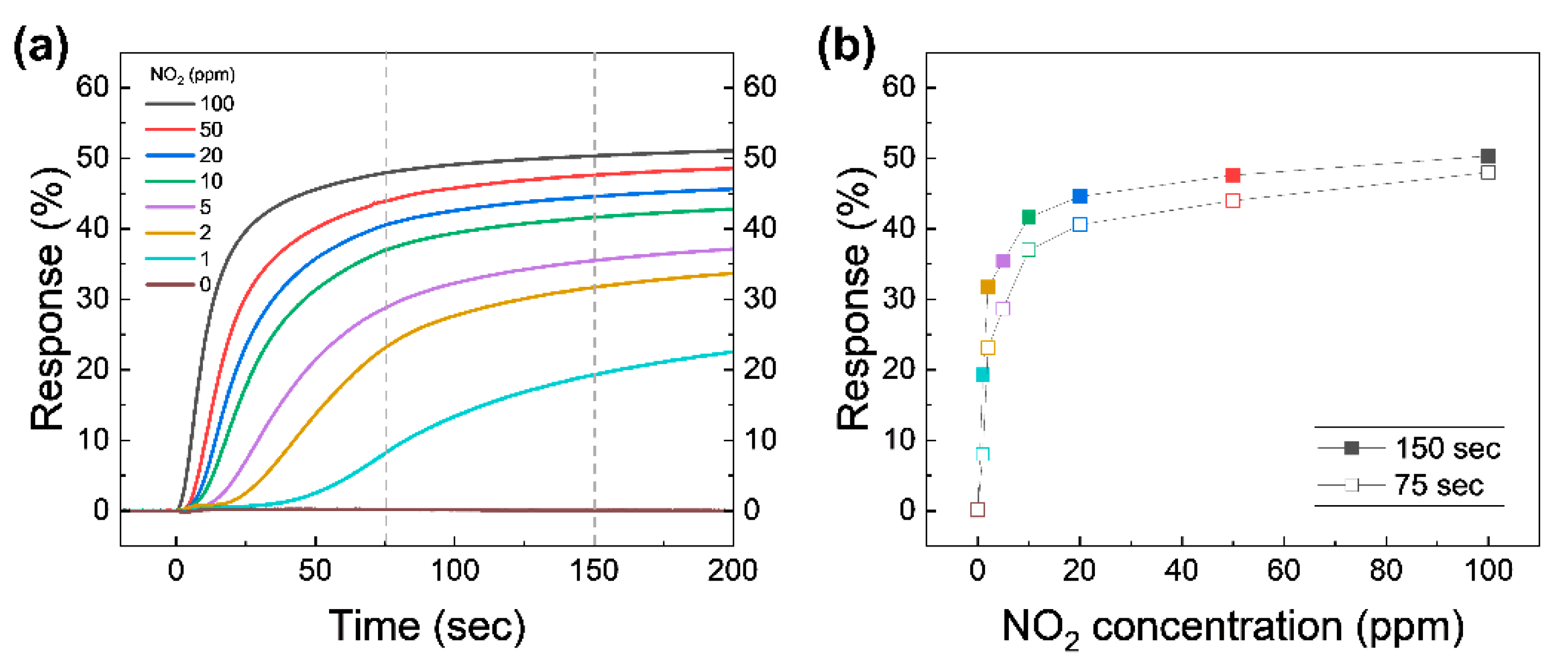
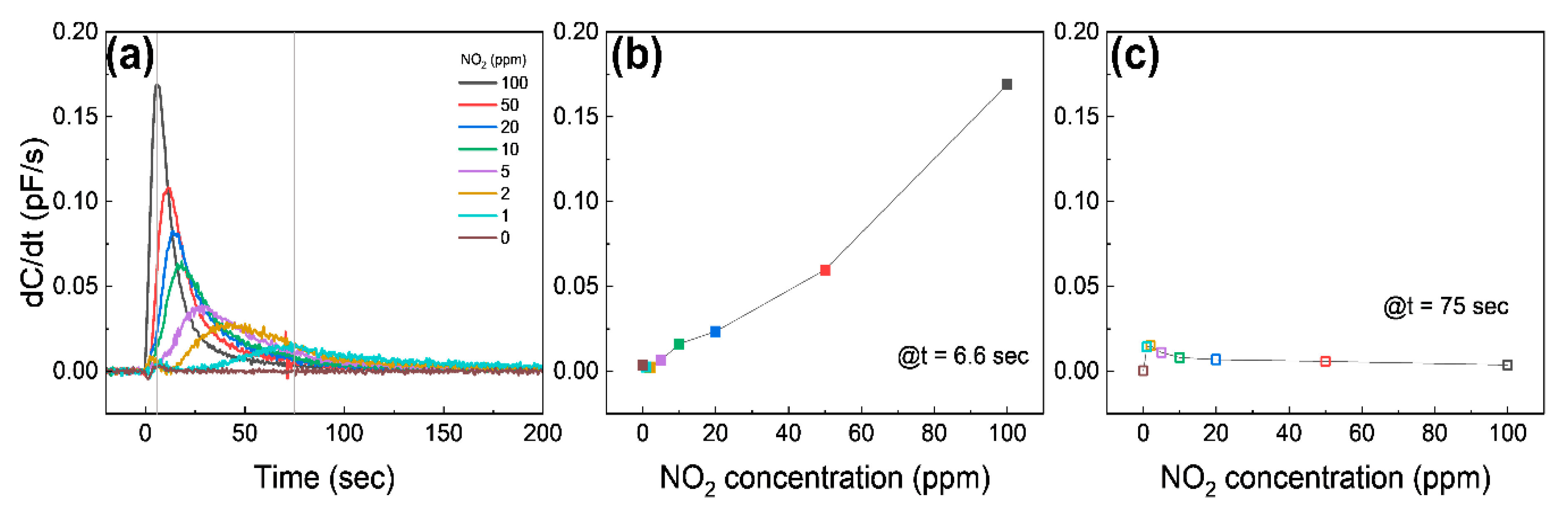
3. Results and Discussion

To evaluate the NO2 sensing performance, the real-time capacitive response of the device at different NO2 concentrations was investigated, as shown in Figure 4a. This is the collection of capacitance response data acquired during the early period of stage ➁ under various NO2 concentrations. Note that actual measured capacitance for calculating the response in Figure 4a is shown in Figure S2 in the Supplementary Material. As illustrated in previous section, the test chamber starts to be filled with NO2 with a desired concentration from 1 to 100 ppm while measuring the capacitance in real-time. The t = 0 value in Figure 4a is set to the beginning of the gas injection. The initial value of capacitance (before the beginning of gas injection) for all trials was set to an almost constant value for a fair comparison. The overall capacitive response increases proportionally to the concentration of NO2 after the test chamber is filled with the test gas. The NO2 molecules in the test chamber adhere to the graphene surface and act as electron acceptors; they attracts electrons from graphene, leaving holes [17]. The hole density causes the increased CQ of the graphene exposed to NO2, because CQ of graphene is proportional to the square root of the carrier density of graphene [28]. The measured capacitance is the series connection of Cgeo of AlOx and CQ of graphene. This leads to changes in the measured capacitance of the device. The capacitive response immediately increases after the relatively high concentrations of 10–100 ppm NO2 are injected into the test chamber. On the other hand, the response to the relatively low concentrations of 1–5 ppm NO2 begins to change in a few seconds. Relatively high concentrations of NO2 are enough to dope graphene at the moment of the injection, so the response graph shows a dramatic change in value at the very early stages of exposure. The response at low concentrations of NO2 takes some time to dope graphene since, NO2 molecules in diluted gases are not enough to dope graphene at the moment of the injection. However, at the lower concentrations, our device can detect the differences in concentrations with higher precision within a moderately allowed time interval.
The response values at t = 75 s (roughly when the chamber pressure reaches atmospheric pressure) and 150 s are plotted as a function of NO2 concentration, as shown in Figure 4b. The response at 75 s proportionally increases with increasing NO2 concentration in the two regions, namely 1–5 and 10–100 ppm. Although the response time under the higher NO2 concentration mixture is much faster simply due to the introduction of the large number of NO2 molecules in the system, the slope of response graph for lower concentrations (1–5 ppm) at the early stages of exposure is greater compared to that of larger concentration cases (10–100 ppm), which means the change in response provides a more precise distinction between various NO2 concentrations below 10 ppm. We believe that this distinction is drawn simply due to the total number of NO2 molecules our device can hold, and that the numbers can be modulated further by redesigning the size of the active channel. The change in the slope shown in Figure 4b can be explained by a shift in Ctotal as a function of the VG curves. A detailed discussion will be given later. The response at 150 s (solid symbols) is increased with a similar trend to the response at 75 s. The changes between 75 and 150 s at high NO2 concentrations are lower than the low concentrations, which means that the response at high concentrations saturates faster than at low concentrations. To make sure of the effect of the pure N2 as a diluent gas, the response of 0 ppm NO2 was tested. When the test chamber was filled with pure N2, the response was changed by lower than 0.1% for 200 s. Impurities (the rest of 99.999% N2) in pure N2 do not significantly affect the capacitive sensing for 200 s, confirming that the N2 is only used to dilute 100 ppm NO2.
Figure 5a shows the different sensing behavior of the differential capacitance (dC/dt) as a function of time. Once the graphene is exposed to 10–100 ppm NO2, dC/dt starts to immediately increase until it reaches the maximum, and then it approaches 0; on the other hand, dC/dt exposed to 1–5 ppm NO2 shows a relatively slowly increase to the maximum and then approaches 0. The dC/dt at 6.6 s (at the maximum value of dC/dt at 100 ppm NO2) is shown in Figure 5b. The dC/dt is a nearly linear relation with the NO2 concentration, suggesting that the device can detect a high concentration of NO2 by measuring dC/dt at the early stage. Figure 5c shows dC/dt at the moment the pressure of the chamber reaches atmospheric pressure (75 s). The dC/dt has an inversely linear relation with NO2 concentrations, except for 0 ppm, which is a different result from Figure 5b. These indicate that the capacitive response at the high NO2 concentration saturates faster than at the low NO2 concentration, as expected.
Response change for an up to 2 h time span is shown in Figure 6a. Note that the response curves in Figure 4a depict the early part of the response change in Figure 6a (up to 200 s). After some time, the responses at all concentrations seemingly exhibit no significant change. It is probably the best time to address the fact that the capacitive response presented in this research shows faster responses compared to the current response given in Figure S3a. Even though the response in current measurements seems a lot higher in values when fully saturated, the capacitive measurements show sharper changes at the initial response, one of the most essential features that the industry requires when it comes to detecting hazardous molecules at the earliest possible stage. This becomes clearer when the gate voltage-dependent capacitance in Figure 6b is compared to the gate voltage-dependent drain current presented in Figure S4 near the Dirac point. The curvature means how sharply a curve bends at a given point; the higher the curvature, the more bent the curve is. The curvature of the gate-dependent current and capacitance shows a peak at the Dirac point voltage as shown in Figure S5a,b, respectively. The full width at half maximum (FWHM) of the capacitance curvature is smaller than the FWHM of the current curvature. The gate-dependent capacitance is more sharply curved in a narrower range near the Dirac point, indicating the greater detection possibility at the very early stages of NO2 introductions into the system.
The response at 0 ppm NO2 (99.999% N2) is almost constant for approximately 15 min after the test chamber is filled. The response starts to slowly increase after a quarter hour. We speculate that 99.999% N2 as a diluent containing 0.001% unexpected impurities acting as acceptors slowly dopes graphene. However, when 100 ppm NO2 is diluted by 99.999% N2, responses of 1–50 ppm NO2 (even with smaller concentrations) do not increase after a quarter hour, indicating that NO2 is binding with graphene far more strongly compared to any other possible impurities that might be present in the balancing gas (N2). This also suggests that N2 is a proper diluent for adjusting NO2 concentration in this test.
Figure 6b shows the gate voltage-dependent Ctotal from 2 V to −2 V after finishing the NO2 sensing measurement (in 2 h), in order to extract carrier density and change in potential fluctuations induced by adsorbed NO2 molecules [29,33,39]. The absorbed NO2 molecules shift the Dirac point voltage (VDP) to the positive gate voltage side and causes a rounding of the curves near the VDP, which is the voltage with the minimum Ctotal. The shift in VDP can reasonably be explained by charge transfer between the graphene and NO2 molecules [36]. Adsorbed NO2 molecules act as electron acceptors, which perform a similar function as the applied negative gate voltage [40].
The upward shift of the Ctotal curves is attributed to the enhancement of local geometrical capacitance caused by NO2 molecules near graphene. The NO2 molecules which are polar molecules can be intercalated between graphene and the Al electrode, similar to intercalated H2O molecules between a substrate and graphene [25]. The intercalated NO2 molecules enhance the effective dielectric constant of the insulating layer in the graphene/AlOx/Al capacitor. The NO2 molecules on graphene are also one of possible contributions to the enhanced electric field originating from the gate electrode. Due to the low density of the state of graphene, the graphene does not screen all of the electric field, which affects NO2 molecules on graphene when Cgeo is comparable to the minimum CQ. The NO2 molecules on the graphene are aligned by the penetrated electric field, resulting in the enhancement of the effective geometrical capacitance.
The Ctotal curves in Figure 6b support the response curve in Figure 4a (also Figure 6a). As NO2 concentration in the chamber increases, the capacitance curves shift up to the right, resulting in changes in Ctotal at VBG = 0 V. This is the mechanism of capacitive NO2 sensing. The dramatic change in the Ctotal curve at 0 ppm near VDP explains the slope in the two regions in Figure 4b. Furthermore, ΔR1ppm (the difference between the response with 1 ppm and the response with 0 ppm) after 2 h exposure is 23.8%, suggesting that the device can detect sub-ppm NO2 through the capacitance measurement. The expected response at concentrations between 0 ppm and 1 ppm would be between 11.8% and 35.6%.
To investigate the electronic properties of NO2 adsorbed graphene, the gate voltage-dependent Ctotal in Figure 6b was fitted using the microscopic model of quantum capacitance in graphene suggested by Xu et al. [39], with Cgeo, parasitic capacitance, and δV (potential variance) as fitting parameters [29]. The extracted δV of graphene exposed to NO2 for 2 h as a function of NO2 concertation is plotted in Figure 6c. Charge transfer between graphene and NO2 molecules causes a local potential fluctuation near the adsorbed NO2 molecules. Since the local potential fluctuations are affected by charged impurities near graphene, such as the density of adsorbed NO2 molecules, δV becomes higher as NO2 concentration increases. In addition, the residual carrier densities were calculated from the quantum capacitance minimum extracted from fitting using the equation C Q = 2 e 2 n / ( v F π ) . The residual carrier density has a similar trend to the potential variation. The results confirm that adsorbed NO2 molecules cause charge transfer from graphene and produce potential fluctuation. Holes produced from the charge transfer shift the VDP to the right. The potential fluctuations round the capacitance curve near VDP. These changes are determined by absorbed NO2 molecules and explain changes in the capacitance at zero gate voltage in Figure 4a (also Figure 6a).

4. Conclusions

In this study, Al back-gated G-FET was fabricated to measure capacitive NO2 sensing performance and the electronic properties of NO2 adsorbed graphene. The quantum capacitance effect caused by enhanced Cgeo of naturally oxidized Al allowed for capacitive sensing. The capacitance of the device exposed to 1–100 ppm NO2 was changed by 21–51% compared to the initial capacitance at t = 150 s. The ΔR1ppm at t = 150 s is 21%, indicating that the device would detect sub-ppm NO2 by the capacitance measurement of the device. Furthermore, the capacitive NO2 sensing mechanism is explained by the gate voltage-dependent Ctotal. Adsorbed NO2 molecules on the graphene surface shift VDP as a function of concentrations of NO2. Carrier density and potential variations in the device caused by absorbed NO2 molecules were extracted from quantum capacitance by fitting. These results demonstrate the fundamental understanding of the absorbed NO2 effect on graphene from capacitance measurement, as well as that capacitive NO2 sensing is possible by enhancing the Cgeo of graphene-based devices.

Supplementary Materials

The following supporting information can be downloaded at: https://www.mdpi.com/article/10.3390/nano13020243/s1, Figure S1: Raman shift for the inspection of the graphene sheet in the device; Figure S2: Changes in Ctotal used for the calculation of the response; Figure S3: Current response of the device exposed to NO2; Figure S4: Gate voltage-dependent current of the device exposed to NO2; Figure S5: Curvatures in gate-dependent current and capacitance. References [41,42] are cited in the supplementary materials.

Author Contributions

Conceptualization, W.J. and S.L.; Methodology, W.J. and S.L.; Formal analysis, W.J. and S.L.; Investigation, W.J.; Data curation, W.J. and S.L.; Writing—original draft, W.J. and S.L.; Writing—review & editing, W.J. and S.L.; Visualization, W.J. and S.L.; Supervision, S.L.; Project administration, S.L.; Funding acquisition, S.L. All authors have read and agreed to the published version of the manuscript.

Funding

This work was supported by the GIST Research Project grant, funded by the GIST in 2022.

Data Availability Statement

Not applicable.

Conflicts of Interest

The authors declare no conflict of interest.

References

  1. Novoselov, K.S.; Geim, A.K.; Morozov, S.V.; Jiang, D.; Zhang, Y.; Dubonos, S.V.; Grigorieva, I.V.; Firsov, A.A. Electric field effect in atomically thin carbon films. Science 2004, 306, 666–669. [Google Scholar] [CrossRef] [PubMed] [Green Version]
  2. Neto, A.C.; Guinea, F.; Peres, N.M.; Novoselov, K.S.; Geim, A.K. The electronic properties of graphene. Rev. Mod. Phys. 2009, 81, 109. [Google Scholar] [CrossRef] [Green Version]
  3. Bonaccorso, F.; Sun, Z.; Hasan, T.; Ferrari, A.C. Graphene photonics and optoelectronics. Nat. Photonics 2010, 4, 611–622. [Google Scholar] [CrossRef] [Green Version]
  4. Chen, C.; Rosenblatt, S.; Bolotin, K.I.; Kalb, W.; Kim, P.; Kymissis, I.; Stormer, H.L.; Heinz, T.F.; Hone, J. Performance of monolayer graphene nanomechanical resonators with electrical readout. Nat. Nanotechnol. 2009, 4, 861–867. [Google Scholar] [CrossRef] [Green Version]
  5. Geim, A.K.; Novoselov, K.S. The rise of graphene. In Nanoscience and Technology: A Collection of Reviews from Nature Journals; World Scientific: Singapore, 2010; pp. 11–19. [Google Scholar]
  6. Zhao, X.; He, D.; You, B. Laser engraving and punching of graphene films as flexible all-solid-state planar micro-supercapacitor electrodes. Mater. Today Sustain. 2022, 17, 100096. [Google Scholar] [CrossRef]
  7. Zheng, C.L.; Zhang, J.L.; Zhang, Q.; You, B.; Chen, G.L. Three dimensional Ni foam-supported graphene oxide for binder-free pseudocapacitor. Electrochim. Acta 2015, 152, 216–221. [Google Scholar] [CrossRef]
  8. Schedin, F.; Geim, A.K.; Morozov, S.V.; Hill, E.W.; Blake, P.; Katsnelson, M.I.; Novoselov, K.S. Detection of individual gas molecules adsorbed on graphene. Nat. Mater. 2007, 6, 652–655. [Google Scholar] [CrossRef]
  9. Dan, Y.; Lu, Y.; Kybert, N.J.; Luo, Z.; Johnson, A.T. Intrinsic response of graphene vapor sensors. Nano Lett. 2009, 9, 1472–1475. [Google Scholar] [CrossRef] [Green Version]
  10. Wang, T.; Huang, D.; Yang, Z.; Xu, S.; He, G.; Li, X.; Hu, N.; Yin, G.; He, D.; Zhang, L. A Review on Graphene-Based Gas/Vapor Sensors with Unique Properties and Potential Applications. Nanomicro Lett. 2016, 8, 95–119. [Google Scholar] [CrossRef] [Green Version]
  11. Pourasl, A.H.; Ahmadi, M.T.; Ismail, R.; Gharaei, N. Gas adsorption effect on the graphene nanoribbon band structure and quantum capacitance. Adsorpt.-J. Int. Adsorpt. Soc. 2017, 23, 767–777. [Google Scholar] [CrossRef]
  12. Alzate-Carvajal, N.; Luican-Mayer, A. Functionalized Graphene Surfaces for Selective Gas Sensing. ACS Omega 2020, 5, 21320–21329. [Google Scholar] [CrossRef] [PubMed]
  13. Ma, J.; Zhang, M.; Dong, L.X.; Sun, Y.B.; Su, Y.J.; Xue, Z.Y.; Di, Z.F. Gas sensor based on defective graphene/pristine graphene hybrid towards high sensitivity detection of NO2. AIP Adv. 2019, 9, 075207. [Google Scholar] [CrossRef] [Green Version]
  14. Zhang, H.; Fan, L.; Dong, H.; Zhang, P.; Nie, K.; Zhong, J.; Li, Y.; Guo, J.; Sun, X. Spectroscopic Investigation of Plasma-Fluorinated Monolayer Graphene and Application for Gas Sensing. ACS Appl Mater Interfaces 2016, 8, 8652–8661. [Google Scholar] [CrossRef] [PubMed]
  15. Zhang, Y.H.; Han, L.F.; Xiao, Y.H.; Jia, D.Z.; Guo, Z.H.; Li, F. Understanding dopant and defect effect on H2S sensing performances of graphene: A first-principles study. Comput. Mater. Sci. 2013, 69, 222–228. [Google Scholar] [CrossRef]
  16. Guo, L.F.; Li, T. Sub-ppb and ultra selective nitrogen dioxide sensor based on sulfur doped graphene. Sens. Actuators B-Chem. 2018, 255, 2258–2263. [Google Scholar] [CrossRef]
  17. Leenaerts, O.; Partoens, B.; Peeters, F. Adsorption of H2O, NH3, CO, NO2, and NO on graphene: A first-principles study. Phys. Rev. B 2008, 77, 125416. [Google Scholar] [CrossRef] [Green Version]
  18. Faustini, A.; Rapp, R.; Forastiere, F. Nitrogen dioxide and mortality: Review and meta-analysis of long-term studies. Eur. Respir. J. 2014, 44, 744–753. [Google Scholar] [CrossRef] [Green Version]
  19. Mills, I.C.; Atkinson, R.W.; Kang, S.; Walton, H.; Anderson, H. Quantitative systematic review of the associations between short-term exposure to nitrogen dioxide and mortality and hospital admissions. BMJ Open 2015, 5, e006946. [Google Scholar] [CrossRef]
  20. Li, Q.F.; Liu, W.H.; Cao, G.M.; Li, X.; Wang, X.L. A study of gas sensing behavior of metal-graphene contact with transfer length method. Appl. Phys. Lett. 2016, 108, 221604. [Google Scholar] [CrossRef]
  21. Kodu, M.; Berholts, A.; Kahro, T.; Avarmaa, T.; Kasikov, A.; Niilisk, A.; Alles, H.; Jaaniso, R. Highly sensitive NO2 sensors by pulsed laser deposition on graphene. Appl. Phys. Lett. 2016, 109, 113108. [Google Scholar] [CrossRef]
  22. Yan, X.; Wu, Y.; Li, R.; Shi, C.; Moro, R.; Ma, Y.; Ma, L. High-Performance UV-Assisted NO2 Sensor Based on Chemical Vapor Deposition Graphene at Room Temperature. ACS Omega 2019, 4, 14179–14187. [Google Scholar] [CrossRef] [PubMed] [Green Version]
  23. Park, S.; Park, M.; Kim, S.; Yi, S.G.; Kim, M.; Son, J.; Cha, J.; Hong, J.; Yoo, K.H. NO2 gas sensor based on hydrogenated graphene. Appl. Phys. Lett. 2017, 111, 213102. [Google Scholar] [CrossRef]
  24. Zhang, Y.; Ma, R.; Zhen, X.V.; Kudva, Y.C.; Buhlmann, P.; Koester, S.J. Capacitive Sensing of Glucose in Electrolytes Using Graphene Quantum Capacitance Varactors. ACS Appl. Mater. Interfaces 2017, 9, 38863–38869. [Google Scholar] [CrossRef] [PubMed]
  25. Olson, E.J.; Ma, R.; Sun, T.; Ebrish, M.A.; Haratipour, N.; Min, K.; Aluru, N.R.; Koester, S.J. Capacitive Sensing of Intercalated H2O Molecules Using Graphene. ACS Appl. Mater. Interfaces 2015, 7, 25804–25812. [Google Scholar] [CrossRef] [Green Version]
  26. Deen, D.A.; Olson, E.J.; Ebrish, M.A.; Koester, S.J. Graphene-based quantum capacitance wireless vapor sensors. IEEE Sens. J. 2013, 14, 1459–1466. [Google Scholar] [CrossRef] [Green Version]
  27. Ma, R.; Su, Q.; Li, J.; Koester, S.J. Acetone sensing using graphene quantum capacitance varactors. In Proceedings of the 2016 IEEE SENSORS, Orlando, FL, USA, 30 October 2016–3 November 2016; pp. 1–3. [Google Scholar]
  28. Xia, J.; Chen, F.; Li, J.; Tao, N. Measurement of the quantum capacitance of graphene. Nat. Nanotechnol. 2009, 4, 505–509. [Google Scholar] [CrossRef]
  29. Ju, W.; Lee, S. Al back-gated graphene field-effect transistors for capacitive sensing applications based on quantum capacitance effect. AIP Adv. 2022, 12, 095210. [Google Scholar] [CrossRef]
  30. Dröscher, S.; Roulleau, P.; Molitor, F.; Studerus, P.; Stampfer, C.; Ensslin, K.; Ihn, T. Quantum capacitance and density of states of graphene. Appl. Phys. Lett. 2010, 96, 152104. [Google Scholar] [CrossRef] [Green Version]
  31. Li, W.; Chen, X.L.; Wang, L.; He, Y.H.; Wu, Z.F.; Cai, Y.; Zhang, M.W.; Wang, Y.; Han, Y.; Lortz, R.W.; et al. Density of States and Its Local Fluctuations Determined by Capacitance of Strongly Disordered Graphene. Sci. Rep. 2013, 3, 1772. [Google Scholar] [CrossRef] [Green Version]
  32. Prado, M.C.; Jariwala, D.; Marks, T.J.; Hersam, M.C. Optimization of graphene dry etching conditions via combined microscopic and spectroscopic analysis. Appl. Phys. Lett. 2013, 102, 193111. [Google Scholar] [CrossRef]
  33. Nagashio, K.; Nishimura, T.; Toriumi, A. Estimation of residual carrier density near the Dirac point in graphene through quantum capacitance measurement. Appl. Phys. Lett. 2013, 102, 173507. [Google Scholar] [CrossRef] [Green Version]
  34. Yang, C.-M.; Chen, T.-C.; Yang, Y.-C.; Meyyappan, M. Annealing effect on UV-illuminated recovery in gas response of graphene-based NO 2 sensors. RSC Adv. 2019, 9, 23343–23351. [Google Scholar] [CrossRef] [PubMed] [Green Version]
  35. Yang, S.X.; Jiang, C.B.; Wei, S.H. Gas sensing in 2D materials. Appl. Phys. Rev. 2017, 4, 021304. [Google Scholar] [CrossRef]
  36. Yavari, F.; Castillo, E.; Gullapalli, H.; Ajayan, P.M.; Koratkar, N. High sensitivity detection of NO2 and NH3 in air using chemical vapor deposition grown graphene. Appl. Phys. Lett. 2012, 100, 203120. [Google Scholar] [CrossRef]
  37. Luo, Z.T.; Pinto, N.J.; Davila, Y.; Johnson, A.T.C. Controlled doping of graphene using ultraviolet irradiation. Appl. Phys. Lett. 2012, 100, 253108. [Google Scholar] [CrossRef]
  38. Imamura, G.; Saiki, K. UV-irradiation induced defect formation on graphene on metals. Chem. Phys. Lett. 2013, 587, 56–60. [Google Scholar] [CrossRef]
  39. Xu, H.L.; Zhang, Z.Y.; Peng, L.M. Measurements and microscopic model of quantum capacitance in graphene. Appl. Phys. Lett. 2011, 98, 133122. [Google Scholar] [CrossRef]
  40. Pinto, H.; Markevich, A. Electronic and electrochemical doping of graphene by surface adsorbates. Beilstein J. Nanotechnol. 2014, 5, 1842–1848. [Google Scholar] [CrossRef] [Green Version]
  41. Wei, J.; Liang, B.; Cao, Q.; Ren, H.; Zheng, Y.; Ye, X. Understanding asymmetric transfer characteristics and hysteresis behaviors in graphene devices under different chemical atmospheres. Carbon 2020, 156, 67–76. [Google Scholar] [CrossRef]
  42. Wang, H.; Wu, Y.; Cong, C.; Shang, J.; Yu, T. Hysteresis of electronic transport in graphene transistors. ACS Nano 2010, 4, 7221–7228. [Google Scholar] [CrossRef]
Figure 1. (a) Cross-sectional view of the device. The red dashed box represents the active capacitor area. (b) Optical microscope image of the fabricated device. The graphene channel is marked with white dashed lines. The scale bar is 15 μm.
Nanomaterials 13 00243 g001
Figure 2. Schematic diagrams of the gas sensing measurement setup.
Nanomaterials 13 00243 g002
Figure 3. An example of a single measurement process consisting of ‘Response’ period, ‘Ctotal vs. VBG’ period, and ‘Recovery’ period. Detailed explanations for each stage number from ➀ to ➅ are given in Section 2.3.
Nanomaterials 13 00243 g003
Figure 4. (a) Capacitive response as a function of time for various NO2 concentrations. Atmospheric pressure is reached in 75 s. The gray vertical dashed lines are marked at 75 and 150 s for comparison. (b) The response at t = 75 s (reached atmospheric pressure; open symbols) and 150 s (closed symbols) from (a) as a function of the NO2 concentration.
Nanomaterials 13 00243 g004
Figure 5. (a) Differential capacitance as a function of time at different NO2 concentrations. The gray solid lines are at 6.6 s and 75 s, respectively. (b,c) show the differential capacitance at 6.6 s and 75 s from (a), respectively.
Nanomaterials 13 00243 g005
Figure 6. (a) Capacitive response at different NO2 concentrations for approximately 2 h. (b) Ctotal as a function of VBG 2 h after exposure to different NO2 concentrations. (c) Extracted residual carrier density and potential variance from (b).
Nanomaterials 13 00243 g006
Disclaimer/Publisher’s Note: The statements, opinions and data contained in all publications are solely those of the individual author(s) and contributor(s) and not of MDPI and/or the editor(s). MDPI and/or the editor(s) disclaim responsibility for any injury to people or property resulting from any ideas, methods, instructions or products referred to in the content.

