Article

Sol–Gel-Processed Y2O3 Multilevel Resistive Random-Access Memory Cells for Neural Networks

1
School of Electronic and Electrical Engineering, Kyungpook National University, Daegu 41566, Republic of Korea
2
The Institute of Electronic Technology, Kyungpook National University, Daegu 41566, Republic of Korea
3
School of Electronics and Information Engineering, Korea Aerospace University, Goyang 10540, Republic of Korea
*
Authors to whom correspondence should be addressed.
Nanomaterials 2023, 13(17), 2432; https://doi.org/10.3390/nano13172432
Submission received: 23 July 2023 / Revised: 17 August 2023 / Accepted: 24 August 2023 / Published: 27 August 2023
(This article belongs to the Special Issue Nanostructures for Integrated Devices)

Abstract

:
Yttrium oxide (Y2O3) resistive random-access memory (RRAM) devices were fabricated using the sol–gel process on indium tin oxide/glass substrates. These devices exhibited conventional bipolar RRAM characteristics without requiring a high-voltage forming process. The effect of current compliance on the Y2O3 RRAM devices was investigated, and the results revealed that the resistance values gradually decreased with increasing set current compliance values. By regulating these values, the formation of pure Ag conductive filament could be restricted. The dominant oxygen ion diffusion and migration within Y2O3 leads to the formation of oxygen vacancies and Ag metal-mixed conductive filaments between the two electrodes. The filament composition changes from pure Ag metal to Ag metal mixed with oxygen vacancies, which is crucial for realizing multilevel cell (MLC) switching. Consequently, intermediate resistance values were obtained, which were suitable for MLC switching. The fabricated Y2O3 RRAM devices could function as a MLC with a capacity of two bits in one cell, utilizing three low-resistance states and one common high-resistance state. The potential of the Y2O3 RRAM devices for neural networks was further explored through numerical simulations. Hardware neural networks based on the Y2O3 RRAM devices demonstrated effective digit image classification with a high accuracy rate of approximately 88%, comparable to the ideal software-based classification (~92%). This indicates that the proposed RRAM can be utilized as a memory component in practical neuromorphic systems.

1. Introduction

Nonvolatile resistive random-access memory (RRAM) is a crucial element for the next generation of memory technologies. With its simple sandwich structure, RRAM offers high-speed performance, low power consumption, and exceptional scalability. These advantages help overcome the von Neumann bottleneck and pave the way for neuromorphic computing systems, which aim to mimic the data-processing capabilities of the human brain [1,2,3]. To accommodate large amounts of data within a limited substrate area, the density of memory devices must be considerably increased. Various approaches, such as complex 3D structures such as vertical RRAM or crossbar configurations, have been proposed to achieve higher storage density [4]. However, these methods often entail complex and costly fabrication processes. Alternatively, a simpler approach is to enable MLC operation with a single memory device. Furthermore, in the context of neuromorphic systems that rely on parallel computation, it is essential to emulate biological synapses, which possess analog weight values. In terms of integration density, a nonvolatile memory component with multilevel memory capabilities is best suited to simulate synapses in offline-based neuromorphic systems compared with the performance of conventional digital memory devices. To achieve multilevel cell (MLC) operation, first, a large high-resistance state (HRS)/low-resistance state (LRS) ratio is required for generating more intermediate levels and enhancing the stability of each level during MCL switching operation, allowing for high bit density. In addition, uniform SET/RESET operation and stable endurance characteristics are required. Many new strategies are being developed to enhance resistive switching properties, uniformity, and stability [5,6,7].
Numerous metal oxide materials, including ZrO2, HfO2, TiO2, and Y2O3, have been utilized as active channel layers in RRAM devices [8,9,10,11,12,13,14,15,16,17,18]. Among them, Y2O3 stands out due to its high dielectric constant and large optical band gap, making it a promising high-k candidate for replacing SiO2 in complementary metal-oxide-semiconductor processes in the industry. The fast ion movement within Y2O3 enables rapid RRAM operation. For integrated RRAM arrays, the “sneak path” issue must be addressed. One solution is to combine Y2O3 with a transistor, acting as a selector. Y2O3 layers can also serve as a passivation layer for transistors, ensuring stable operation while simultaneously functioning as an active channel layer for RRAM devices. This approach reduces the number of fabrication steps and enhances cost efficiency [19,20]. Various conventional vacuum-based deposition methods have been used to deposit metal oxide active channel layers. However, these methods are time-consuming and not cost-efficient. In contrast, the sol–gel process is a well-known technique for depositing metal oxide layers using solution-phase precursor solutions. These precursor solutions can be used as ink for printing or spin-coating, allowing for a large-area application at a lower cost [21,22].
Herein, sol–gel-processed Y2O3 films were employed as active channel layers for RRAM devices. The fabricated Y2O3 RRAM devices exhibited conventional bipolar memory operation without requiring a forming process, thanks to the presence of oxygen vacancies with top Ag electrodes. These devices showed a sharp transition from a HRS to a LRS or vice versa. To enable multicell operation, the set current compliance was varied. As the current compliance values increased, the resistance values obtained gradually decreased, resulting in intermediate values within the LRS and HRS suitable for multilevel cell (MLC) switching. In numerical simulations, the Y2O3 RRAM device with multilevel memory states effectively functioned as an artificial synaptic cell with long-term plasticity in offline-learning-based neural networks. The constructed neuromorphic system successfully recognized complex handwritten digit images with an accuracy of approximately 88%. This level of accuracy is comparable to that of an ideal software system.

2. Materials and Methods

Y2O3 RRAM devices were fabricated using a vertically stacked structure comprising glass, indium tin oxide (ITO) bottom electrodes, Y2O3, and Ag top electrodes (TEs). The fabrication process involved several steps:
  • Cleaning the ITO-coated glass substrate: The substrate was immersed in acetone and sonicated for 10 min, followed by additional cleaning with deionized water. A UV/O3 treatment was then performed for 1 h to remove any remaining organic impurities.
  • Y2O3 precursor solution preparation: A Y2O3 precursor solution (0.3 M) was created by dissolving yttrium (III) nitrate tetrahydrate (Y(NO3)34H2O) in 2-methoxymethanol. The solution was sonicated for an additional 10 min to achieve a clear solution.
  • Coating Y2O3 on the ITO/glass substrate: A tiny Kapton tape was used to define the contact window for the ITO bottom electrodes. The Y2O3 precursor solution was then spin-coated onto the cleaned ITO/glass substrate at 3000 rpm for 50 s. The Kapton tape was removed before the heating process.
  • Thermal annealing: To evaporate the solvent, the coated substrate was annealed on a hot plate at 100 °C for 10 min. The coated substrate was thermally annealed in a furnace at 500 °C for 3 h in the presence of air to convert the Y2O3 precursor into Y2O3.
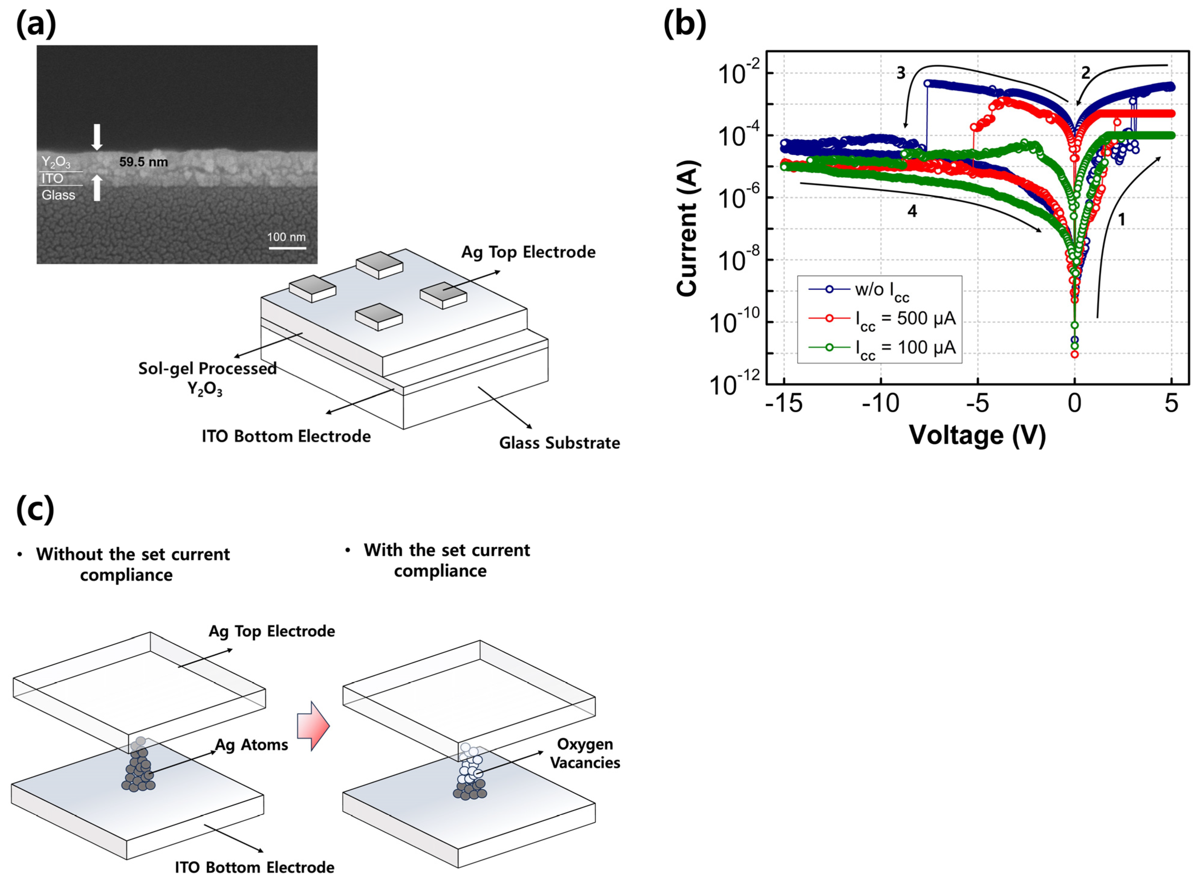
  • Deposition of Ag TE: A shadow metal mask was placed in contact with the Y2O3 film to define the size of the electrode (30 μm × 30 μm). A 100-nm-thick layer of Ag was deposited onto the Y2O3 films using thermal evaporation at a rate of 1.8 Å/s under 5 × 10⁻⁶ torr.
After fabrication, the crystal structure properties of the Y2O3 film were investigated using grazing incidence X-ray diffraction (GIXRD, X’pert Pro, Malvern PANalytical, Malvern, UK; incident angle = 0.3°, Cu-Kα, λ = 1.54 Å). The optical characteristics of the sol–gel processed films were estimated using an UV–visible technique (UV–vis; LAMBDA 265, Waltham, MA, USA). Moreover, a field-emission scanning electron microscope (FE-SEM, Hitachi 8230, Hitachi, Tokyo, Japan) was used to estimate the thickness and surface roughness of the film. The chemical composition analysis was conducted using X-ray photoelectron spectroscopy (XPS; Nexsa, ThermoFisher, Waltham, MA, USA). The electrical characteristics, including the I–V curve, retention, and endurance, were measured at room temperature using a probe station (MST T-4000A, Hwaseong, Korea) and parameter analyzer (Keithley 2636B, Keithley Instruments, Cleveland, OH, USA).

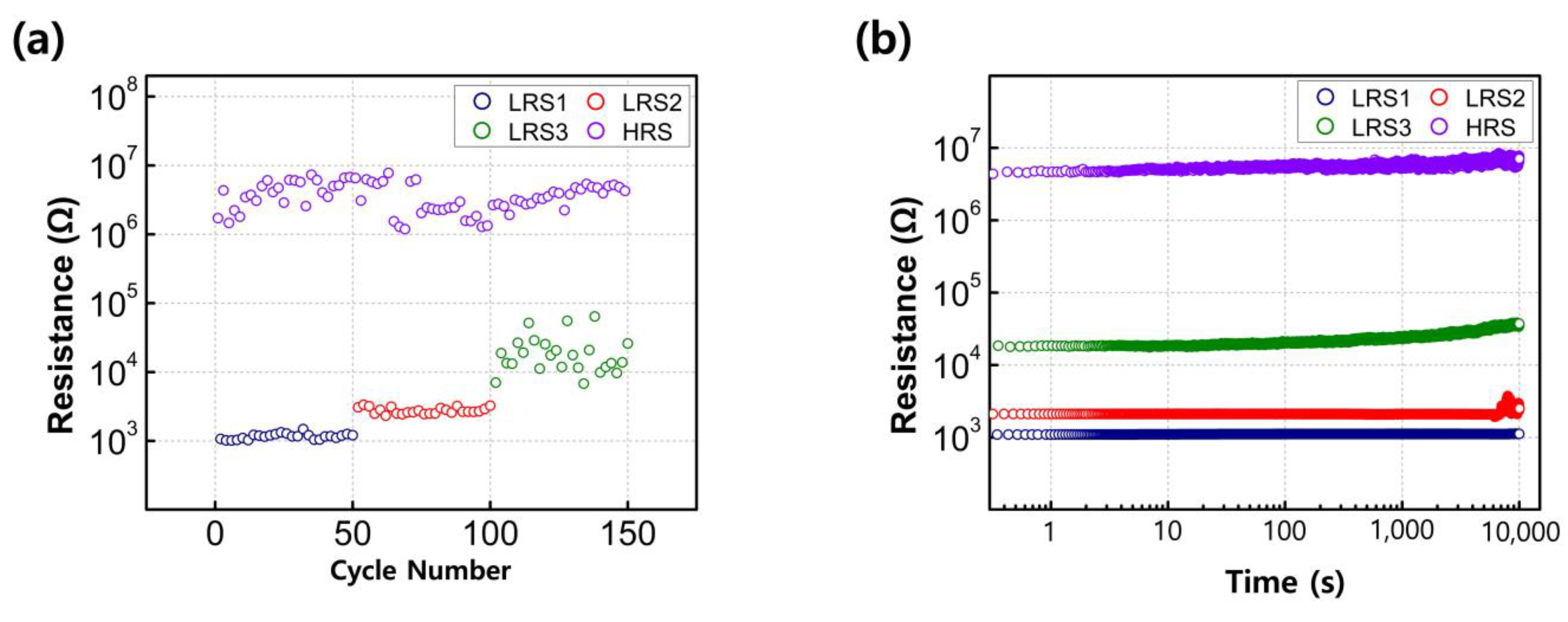
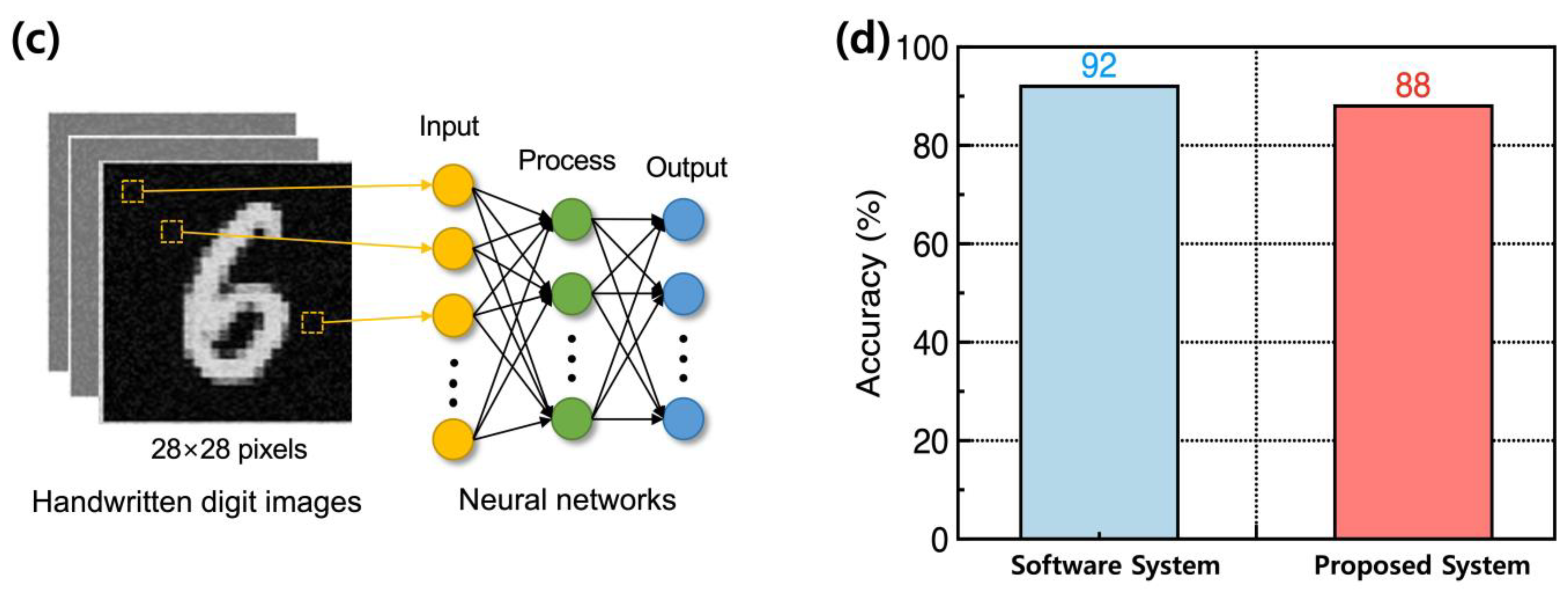
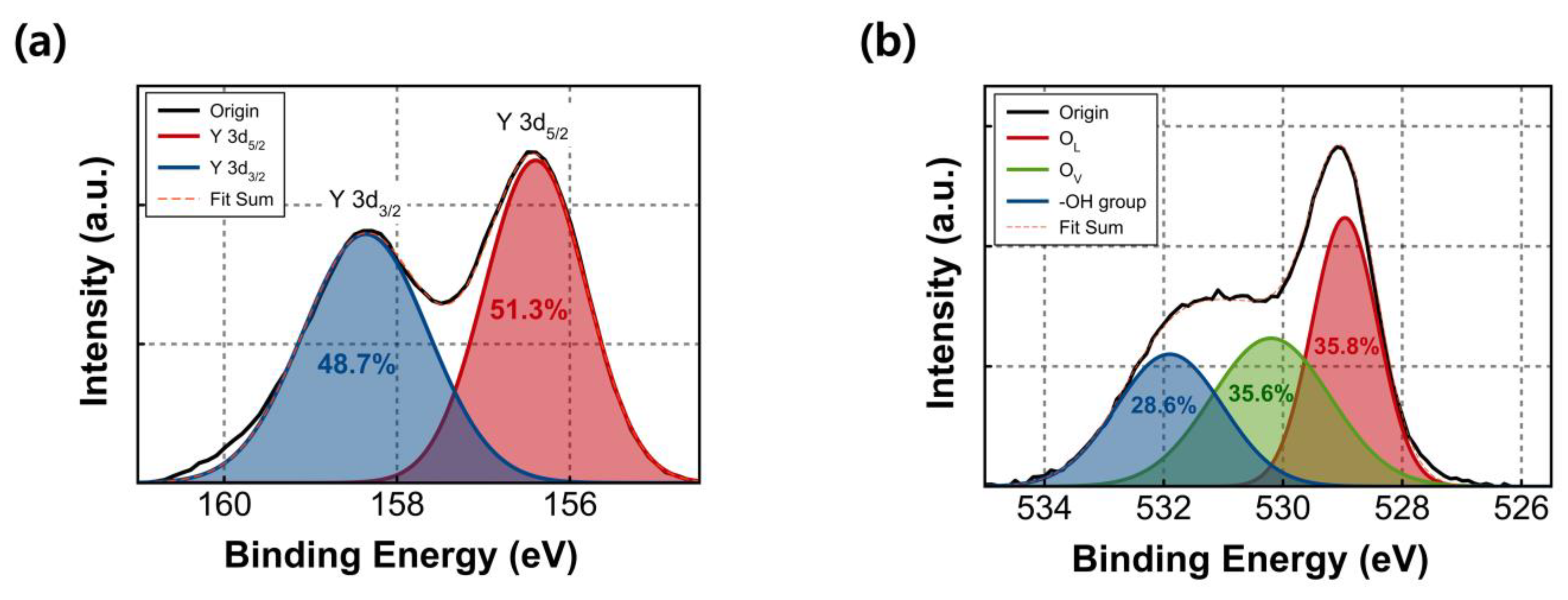
3. Results and Discussion

Figure 1a displays the GIXRD spectra of the Y2O3 film fabricated through the sol–gel method. The diffraction peaks at 2θ angles of 29.30°, 33.96°, 48.79°, and 57.93° correspond to the (222), (400), (440), and (622) crystallographic planes of Y2O3, respectively. Based on the GIXRD results, it is evident that the fabricated Y2O3 film consists entirely of a cubic crystal structure in the polycrystalline phase, specifically conforming to the cubic Y2O3 phase (JCPDS 74-1828). Notably, while a metastable monoclinic Y2O3 phase can form at low temperatures, the dominant phase observed here is the stable cubic Y2O3 phase [23]. The prominent peak at 29.30° indicates that the grains in the film primarily grow in the (222) plane. The crystallite size of the grains can be determined using the Scherrer equation.
D = (0.9 λ)/(β cos θ)
where D, λ, β, and θ represent the crystalline size, CuΚα wavelength, full width at half maximum (FWHM) of the diffraction peak, and Bragg angle, respectively. The grain size of the (222) plane is the largest among the crystallographic planes, as evident from the narrowest FWHM of the diffraction peak at 29.30°. The calculated crystalline size from the (222) plane is 12.23 nm.
The optical characteristics of the Y2O3 film were investigated via ultraviolet–visible spectroscopy (UV–Vis). As shown in Figure 1b, the fabricated film shows a similar transmittance spectrum to that of the cleaned glass sample in the visible range, implying sufficient transparency of the fabricated film. The bandgap of the Y2O3 film can be obtained by extrapolating the linear part of the (ahv)2 versus hv graph. The inset of Figure 1b shows (ahv)2 versus hv derived from the Tauc equation.
(ahv)2 = A(hv − Eg),
where α denotes the absorption coefficient, A is a constant, h is the Planck constant, v is the photon frequency, and Eg is the optical bandgap. The intersection point between the extrapolation line and the x-axis represents the band gap of the Y2O3 film (a large optical band gap of 4.31 eV is observed in this case).
Figure 2 presents the XPS results of the fabricated Y2O3 film, with all binding energy values corrected to the main C 1s peak (284.8 eV). In Figure 2a, the XPS spectra for Y 3d reveal the two splitting orbitals, Y 3d5/2 and Y 3d3/2. The Y 3d5/2 and Y 3d3/2 peaks are located at 156.4 eV and 158.4 eV, respectively, confirming the successful formation of the Y2O3 film on the substrate. The XPS results of Y2O3 film for O 1s are shown in Figure 2b. The deconvoluted O 1s peaks appear at 529.0, 530.2, and 531.9 eV, corresponding to the oxygen lattice (OL), oxygen vacancies (OV), and hydroxyl group (-OH), respectively. The area ratio of the OL peak was 35.8%, while that of the OV peak was 35.6%. These two components are almost equally proportioned in the O 1s spectra.
Figure 3a presents a schematic of the fabricated RRAM devices; the inset shows the cross-sectional SEM image of Y2O3 films on ITO/glass substrates. Figure 3b displays representative I–V characteristics of the fabricated Y2O3 RRAM devices with different levels of compliance current. To observe the set/reset behavior, the voltage of the TE was swept from −15 V to 5 V, with the bottom electrode (BE) grounded. The read voltage was set at 0.1 V. The initially obtained resistance values were relatively high, indicating HRS. At a specific voltage known as the SET voltage, the current abruptly increased, resulting in low-resistance values, referred to as the LRS. When a voltage was applied from positive to negative values, known as the RESET voltage, the LRS turned back into the HRS. Notably, all fabricated Y2O3-based RRAM devices demonstrated apparent bipolar switching behavior without requiring an unwanted forming process. This distinguishes them from OV-rich metal-oxide-based RRAMs or Ag/Cu electrode-based RRAMs, often necessitating an additional forming process [24,25]. The Y2O3 films formed in this study exhibited some oxygen vacancy formation, and the use of Ag TE facilitated the easy formation of conductive filaments (CFs) without the need for a high-voltage forming process. This mechanism is based on conductive bridge random-access memory, which operates through the reduction and oxidation of Ag. Comparisons were made between Y2O3 RRAM devices with Ag TE and those with Au TE. The RRAM with Au TE did not exhibit evident RRAM characteristics since Au cannot form conductive bridges similar to Ag due to its low reactivity [14]. In contrast, the diffusive nature of Ag allowed it to penetrate the switching layer easily, enabling the formation of CFs. In addition, the Y2O3 switching layer contained abundant OV, which facilitated the formation of CFs without the need for applying a forming voltage. During the set process, a negative bias of −15 V was applied to the Ag TE, resulting in the HRS state. Upon applying a positive bias, Ag atoms lost electrons through an oxidation reaction and formed cations (Ag → Ag+ + e). These cations then migrated to the BE and received electrons through a reduction reaction (Ag+ + e → Ag), leading to reduced Ag atoms in the switching layer. Once a particular voltage was reached, the TE and the BE were connected by conductive bridges made of Ag, transitioning the device to LRS. An abrupt increase in current at the SET voltage corresponds to the set process. Conversely, when the voltage applied to the TE was swept toward −15 V, the current dropped suddenly at the RESET voltage. This is attributed to the oxidation reaction of the Ag atoms, facilitated by a thermal electrochemical process. The oxidized Ag cations then returned to the TE, causing the conductive bridges to dissolve, thereby disconnecting the TE and the BE and returning the device to its initial HRS state.
When the fabricated RRAM device is operated without the set current compliance, the device experiences abrupt SET and RESET behaviors during positive and negative sweep cycles, respectively. With decreasing set current compliance values, the device experiences smooth SET and RESET behaviors during positive and negative sweep cycles, respectively. In our previous study, we confirmed that RRAM devices with an Ag/Y2O3/ITO structure are conductive bridge random-access memory devices, which rely on the migration of metal ions. Simultaneously, oxygen vacancy sites can also serve as pathways for filament formation because Ag ions can migrate through these sites with lower migration barriers, requiring less energy for movement. This behavior, affected by the set current compliance values, originates from the control of Ag filament generation. Without any set current compliance, the formed conductive filament is dominated by Ag. With decreasing set current compliance values, a portion of Ag is reduced, and OV dominates the conductive filament. Owing to the restriction of Ag filament, the set current compliance values can be regulated. The dominant oxygen ion diffusion and migration within Y2O3 leads to the formation of OV and Ag metal-mixed CFs between two electrodes. The filament composition changes from pure Ag metal to Ag metal mixed with OV, which is critical for realizing MLC switching by controlling the set current compliance values.
Figure 4a illustrates the cumulative distribution function of the resistance states of the fabricated RRAM devices, programmed by setting different current compliance levels with a read voltage of +0.1 V. With decreasing current compliance values, the fabricated RRAM devices showed the gradual resistance switching characteristics, indicating the formation of OV and Ag metal-mixed CFs between two electrodes. This led to the formation of intermediate resistance values within the LRS and HRS, rendering them suitable for MLC switching. The LRS values are influenced by factors such as the radius of the CFs or the concentration of filaments between the bottom and TEs [26,27]. When a low compliance current is applied to the device, the formation of CFs is suppressed, leading to narrower CFs and a slight increase in the resistance of the switching layer. This phenomenon cannot occur when the conductive filament contains pure Ag filament. Conversely, the HRS values did not exhibit considerable changes, irrespective of the set current compliance value. The HRS values are known to be affected by the distance between the top of the broken CF and the TEs, known as the rupture region distance. The fact that the fabricated Y2O3 RRAM devices did not show considerable HRS variation indicates that the rupture region distance between the top of the broken CF and the TEs was unaffected by the set current compliance values.
With increasing set current compliance values, wider CFs are formed. Breaking thicker CFs, resulting from the reduction process, requires larger RESET voltages. Consequently, as the set compliance current values increase, the RESET voltage also increases [28]. By controlling the current compliance values, the fabricated RRAM devices can operate as a MLC with a capacity of 2 bits in one cell through three LRSs and one common HRS.
To assess the reliability of the fabricated RRAM, endurance and retention tests were conducted under different compliance current conditions. The HRS and LRS values were extracted at a voltage of +0.1 V after programming and erasing operations, each lasting for 50 ms. As shown in Figure 5a, the resistance states of the fabricated RRAM devices, both with and without compliance current conditions, exhibited stable endurance properties for about 50 cycles. The largest on/off ratio was observed under compliance-current-free conditions, with a value of around 103. The read-out margin, array size, and intermediate multilevels were decided by a HRS/LRS ratio [29,30,31]. To increase this ratio, the leakage current should be suppressed under HRS conditions. The leakage current is affected by the film phase, defect concentration, or energy barrier conditions [10,11,18,32]. More investigation is needed. Figure 5b displays the retention characteristics of the four resistance states. The three LRS and one HRS states exhibit excellent MLC behavior, maintaining their resistance values for up to 104 s without any significant degradation.
To assess the capability of the Y2O3 RRAM as a synaptic component with long-term plasticity for the offline-learning-based neural networks, numerical simulations were conducted. Figure 5c illustrates the hardware systems, comprising three distinct neuron layers, constructed to recognize handwritten digit images provided by the Modified National Institute of Standards and Technology. The system involved 784, 512, and 10 neurons for the input, processing, and output signals, respectively. The three layers of neurons were interconnected through artificial synapses. Each single synapse cell in the network comprised five different RRAM devices, and the nonvolatile memory states of these devices were estimated based on the results shown in Figure 5c. During training, optimal distributions of synaptic weights were calculated through software simulation. These weights were then converted into feasible conductance values for the RRAM cell. Figure 5d shows the recognition accuracy of the constructed system after offline training for 60 epochs. The hardware neural networks based on the Y2O3 RRAM devices effectively classified the digit images with a high accuracy of approximately 88%. Although the recognition accuracy of the hardware system was slightly lower than that of the ideal software (about 92%), the recognition accuracy of the system can be simply enhanced by employing a continuous synapse cell comprised of more than five RRAM devices. This demonstrates that the proposed Y2O3 RRAM devices can be utilized as a memory component to achieve practical neuromorphic systems.

4. Conclusions

Sol–gel-processed Y2O3 RRAM devices were successfully fabricated on ITO/glass substrates. These devices exhibit conventional bipolar RRAM characteristics, eliminating the need for a high-voltage forming process. By increasing the set current compliance values, the resistance values obtained gradually decrease, allowing for the realization of intermediate resistance values within the LRS and HRS, rendering them suitable for MLC switching. By regulating the set current compliance values, pure Ag filament conductive filament formation was restricted. The dominant oxygen ion diffusion and migration within Y2O3 leads to the formation of OV and Ag metal–mixed CFs between the two electrodes. The filament composition changes from pure Ag metal to Ag metal with OV, which is critical for realizing the MLC switching. The fabricated devices can effectively operate as an MLC with a capacity of two bits in one cell, utilizing three LRS and one common HRS. When applying a low compliance current to the device, the formation of CF is suppressed, leading to a narrower CF and a slight increase in the resistance of the switching layer. To evaluate the potential of the Y2O3 RRAM devices for neural networks, numerical simulations were conducted. The results demonstrate that hardware neural networks based on the Y2O3 RRAM devices effectively classify digit images with a high accuracy of about 88%. This indicates that the proposed Y2O3 RRAM devices can be utilized as a memory component to achieve practical neuromorphic systems.

Author Contributions

Conceptualization, S.-H.L. and J.J.; experiments and data analysis, T.L., H.-I.K., Y.C., S.L., W.-Y.L. and K.K.; investigation, Y.C., S.L., J.-H.B., I.-M.K. and J.J.; writing—original draft preparation, T.L., S.-H.L. and J.J.; writing—review and editing, S.-H.L., J.-H.B., I.-M.K., K.K. and J.J. All authors have read and agreed to the published version of the manuscript.

Funding

This work was supported by the National Research Foundation of Korea (NRF) grant funded by the Korean government (MSIT) (2022R1A2C1006317) and by the National R&D Program through the National Research Foundation of Korea (NRF) funded by the Ministry of Science and ICT (2021M3F3A2A03017764).

Institutional Review Board Statement

Not applicable.

Informed Consent Statement

Not applicable.

Data Availability Statement

The data are available in a publicly accessible repository.

Conflicts of Interest

The authors declare no conflict of interest.

References

  1. Wang, Z.; Joshi, S.; Savel’ev, S.E.; Jiang, H.; Midya, R.; Lin, P.; Hu, M.; Ge, N.; Strachan, J.P.; Li, Z. Memristors with diffusive dynamics as synaptic emulators for neuromorphic computing. Nat. Mater. 2017, 16, 101–108. [Google Scholar] [CrossRef] [PubMed]
  2. Yoon, J.H.; Wang, Z.; Kim, K.M.; Wu, H.; Ravichandran, V.; Xia, Q.; Hwang, C.S.; Yang, J.J. An artificial nociceptor based on a diffusive memristor. Nat. Commun. 2018, 9, 417. [Google Scholar] [CrossRef] [PubMed]
  3. Jeong, D.S.; Hwang, C.S. Nonvolatile memory materials for neuromorphic intelligent machines. Adv. Mater. 2018, 30, 1704729. [Google Scholar] [CrossRef] [PubMed]
  4. Bai, Y.; Wu, H.; Wu, R.; Zhang, Y.; Deng, N.; Yu, Z.; Qian, H. Study of Multi-level Characteristics for 3D Vertical Resistive Switching Memory. Sci. Rep. 2014, 4, 5780. [Google Scholar] [CrossRef]
  5. Ho, T.-L.; Ding, K.; Lyapunov, N.; Suen, C.-H.; Wong, L.-W.; Zhao, J.; Yang, M.; Zhou, X.; Dai, J.-Y. Multi-Level Resistive Switching in SnSe/SrTiO3 Heterostructure Based Memristor Device. Nanomaterials 2022, 12, 2128. [Google Scholar] [CrossRef]
  6. Park, J.; Park, E.; Yu, H.-Y. Active layer nitrogen doping technique with excellent thermal stability for resistive switching memristor. Appl. Surf. Sci. 2022, 603, 154307. [Google Scholar] [CrossRef]
  7. Wang, S.; Ning, X.; Hao, A.; Chen, R. Metal nanoparticles layer boosted resistive switching property in NiFe2O4-based memory devices. J. Alloys Compd. 2022, 908, 164569. [Google Scholar] [CrossRef]
  8. Jang, J.; Subramanian, V. Effect of electrode material on resistive switching memory behavior of solution-processed resistive switches: Realization of robust multi-level cell. Thin Solid Films 2017, 625, 87–92. [Google Scholar] [CrossRef]
  9. Smith, J.; Chung, S.; Jang, J.; Biaou, C.; Subramanian, V. Solution-processed complementary resistive switching arrays for associative memory. IEEE Trans. Electron Devices 2017, 64, 4310–4316. [Google Scholar] [CrossRef]
  10. Lee, S.; Kim, T.; Jang, B.; Lee, W.Y.; Song, K.C.; Kim, H.S.; Do, G.Y.; Hwang, S.B.; Chung, S.; Jang, J. Impact of device area and film thickness on performance of sol-gel processed ZrO2 RRAM. IEEE Electron. Device Lett. 2018, 39, 668–671. [Google Scholar] [CrossRef]
  11. Ha, S.; Lee, H.; Lee, W.Y.; Jang, B.; Kwon, H.J.; Kim, K.; Jang, J. Effect of annealing environment on the performance of sol-gel-processed ZrO2 RRAM. Electronics 2019, 8, 947. [Google Scholar] [CrossRef]
  12. Kim, K.; Hong, W.; Lee, C.; Lee, W.Y.; Kim, H.J.; Kwon, H.J.; Kang, H.; Jang, J. Sol-gel-processed amorphous-phase ZrO2 Based resistive random-access memory. Mater. Res. Express 2021, 8, 116301. [Google Scholar] [CrossRef]
  13. Ding, Z.; Feng, Y.; Huang, P.; Liu, L.; Kang, J. Low-power resistive switching characteristic in HfO2/TiOx bi-layer resistive random-access memory. Nanoscale Res. Lett. 2018, 14, 157. [Google Scholar] [CrossRef]
  14. Kim, K.; Lee, C.; Lee, W.Y.; Kim, H.J.; Lee, S.H.; Bae, J.H.; Kang, I.M.; Jang, J. Enhanced switching ratio of sol–gel-processed Y2O3 RRAM device by suppressing oxygen-vacancy formation at high annealing temperature. Semicond. Sci. Technol. 2021, 37, 015007. [Google Scholar] [CrossRef]
  15. Kim, D.W.; Kim, H.J.; Lee, W.Y.; Kim, K.; Lee, S.H.; Bae, J.H.; Kang, I.M.; Kim, K.; Jang, J. Enhanced switching reliability of sol–gel-processed Y2O3 RRAM devices based on Y2O3 surface roughness-induced local electric field. Materials 2022, 15, 1943. [Google Scholar] [CrossRef] [PubMed]
  16. Kim, H.J.; Kim, D.W.; Lee, W.Y.; Kim, K.; Lee, S.H.; Bae, J.H.; Kang, I.M.; Kim, K.; Jang, J. Flexible sol-gel-processed Y2O3 RRAM devices obtained via UV/Ozone-assisted photochemical annealing process. Materials 2022, 15, 1899. [Google Scholar] [CrossRef] [PubMed]
  17. Kim, H.I.; Lee, T.; Lee, W.Y.; Kim, K.; Bae, J.H.; Kang, I.M.; Lee, S.H.; Kim, K.; Jang, J. Improved Environment Stability of Y2O3 RRAM Devices with Au Passivated Ag Top Electrodes. Materials 2022, 15, 6859. [Google Scholar] [CrossRef]
  18. Kim, K.; Kim, H.I.; Lee, T.; Lee, W.Y.; Bae, J.H.; Kang, I.M.; Lee, S.H.; Jang, J. Thickness dependence of resistive switching characteristics of the sol–gel processed Y2O3 RRAM devices. Semicond. Sci. Technol. 2023, 38, 045002. [Google Scholar] [CrossRef]
  19. Lee, C.; Lee, W.Y.; Kim, H.J.; Bae, J.H.; Kang, I.M.; Lim, D.; Kim, K.; Jang, J. Extremely bias stress stable enhancement mode sol–gel-processed SnO2 thin-film transistors with Y2O3 passivation layers. Appl. Surf. Sci. 2021, 559, 149971. [Google Scholar] [CrossRef]
  20. Lee, Y.W.; Kim, D.W.; Kim, H.J.; Kim, K.; Lee, S.H.; Bae, J.H.; Kang, I.M.; Kim, K.; Jang, J. Environmentally and electrically stable sol–gel-deposited SnO2 thin-film transistors with controlled passivation layer diffusion penetration depth that minimizes mobility degradation. ACS Appl. Mater. Interfaces 2022, 14, 10558–10565. [Google Scholar] [CrossRef]
  21. Jang, J.; Kang, H.; Chakravarthula, H.C.N.; Subramanian, V. Fully inkjet-printed transparent oxide thin film transistors using a fugitive wettability switch. Adv. Electron. Mater. 2015, 1, 1500086. [Google Scholar] [CrossRef]
  22. Scheideler, W.J.; Jang, J.; Karim, M.A.U.; Kitsomboonloha, R.; Zeumault, Z.; Subramanian, V. Gravure-Printed Sol-Gels on Flexible Glass: A Scalable Route to Additively Patterned Transparent Conductors. ACS Appl. Mater. Interfaces 2015, 7, 12679–12687. [Google Scholar] [CrossRef] [PubMed]
  23. Lim, D.G.; Kwak, D.J.; Yi, J. Improved interface properties of yttrium oxide buffer layer on silicon substrate for ferroelectric random access memory applications. Thin Solid Films 2017, 422, 150–154. [Google Scholar] [CrossRef]
  24. Yang, B.; Xu, N.; Li, C.; Huang, C.; Ma, D.; Liu, J.; Arumi, D.; Fang, L. A forming-free ReRAM cell with low operating voltage. IEICE Electron. Express 2020, 17, 20200343. [Google Scholar] [CrossRef]
  25. Abbas, Y.; Ambade, R.B.; Ambade, S.B.; Han, T.H.; Choi, C. Tailored nanoplateau and nanochannel structures using solution-processed rutile TiO2 thin films for complementary and bipolar switching characteristics. Nanoscale 2019, 11, 13815. [Google Scholar] [CrossRef]
  26. Prakash, A.; Deleruyelle, D.; Song, J.; Bocquet, M.; Hwang, H. Resistance controllability and variability improvement in a TaOx-based resistive memory for multilevel storage application. Appl. Phys. Lett. 2015, 106, 233104. [Google Scholar] [CrossRef]
  27. Sedghi, N.; Li, H.; Brunell, I.F.; Dawson, K.; Potter, R.J.; Guo, Y.; Gibbon, J.T.; Dhanak, V.R.; Zhang, W.D.; Zhang, J.F.; et al. The role of nitrogen doping in ALD Ta2O5 and its influence on multilevel cell switching in RRAM. Appl. Phys. Lett. 2017, 110, 102902. [Google Scholar] [CrossRef]
  28. Kim, D.; Shin, J.; Kim, S. Resistive Switching Characteristics of ZnO-Based RRAM on Silicon Substrate. Metals 2021, 11, 1572. [Google Scholar] [CrossRef]
  29. Deng, Y.; Huang, P.; Chen, B.; Yang, X.; Gao, B.; Wang, J.; Zeng, L.; Du, G.; Kang, J.; Liu, X. RRAM crossbar array with cell selection device: A device and circuit interaction study. IEEE Trans. Electron. Devices 2013, 60, 719–726. [Google Scholar] [CrossRef]
  30. Mahata, C.; Kang, M.; Kim, S. Multi-level analog resistive switching characteristics in tri-layer HfO2/Al2O3/HfO2 based memristor on ITO electrode. Nanomaterials 2020, 10, 2069. [Google Scholar] [CrossRef]
  31. Tseng, H.T.; Hsu, T.H.; Tsai, M.H.; Huang, C.Y.; Huang, C.L. Resistive switching characteristics of sol-gel derived La2Zr2O7 thin film for RRAM applications. J. Alloys Compd. 2022, 899, 163294. [Google Scholar] [CrossRef]
  32. Zhu, X.; Zhuge, F.; Li, M.; Yin, K.; Liu, Y.; Zuo, Z.; Chen, B.; Li, R.W. Microstructure dependence of leakage and resistive switching behaviors in Ce-doped BiFeO3 thin film. J. Phys. D Appl. Phys. 2011, 44, 415104. [Google Scholar] [CrossRef]
Figure 1. (a) GIXRD spectra of sol–gel-processed Y2O3 films and (b) transmittance spectra of sol–gel-processed Y2O3 films; the inset shows (ahv)2 vs. photon energy.
Nanomaterials 13 02432 g001
Figure 2. XPS spectra: (a) Y 3d and (b) O 1s of sol–gel-processed Y2O3 films.
Nanomaterials 13 02432 g002
Figure 3. (a) Schematic of the device; the inset shows the cross-sectional SEM image of Y2O3 films on ITO/glass substrates; and (b) representative IV curves of the fabricated Y2O3 RRAM as a function of the set current compliance values. The arrows and numbers indicate the voltage sweep directions. (c) Schematic of the CF component change without/with the set current compliance.
Nanomaterials 13 02432 g003
Figure 4. Cumulative distribution of resistance states (a) and SET and RESET values (b) for sol–gel-processed Y2O3 RRAM devices.
Nanomaterials 13 02432 g004
Figure 5. Nonvolatile properties of sol–gel-processed Y2O3 RRAM devices as a function of the set current compliance values: (a) endurance and (b) retention. (c) A constructed hardware neural network for classifying the handwritten digit images provided by the Modified National Institute of Standards and Technology. The system is composed of three different neuron layers corresponding to the input (784 neurons), processing (32 neurons), and output (10 neurons) signals. The neuron layers are interconnected through synaptic cells based on Y2O3 RRAM devices. (d) Recognition accuracy values for the ideal software system and the proposed hardware neural network. Each system was tested after training for 60 epochs.
Nanomaterials 13 02432 g005aNanomaterials 13 02432 g005b
Disclaimer/Publisher’s Note: The statements, opinions and data contained in all publications are solely those of the individual author(s) and contributor(s) and not of MDPI and/or the editor(s). MDPI and/or the editor(s) disclaim responsibility for any injury to people or property resulting from any ideas, methods, instructions or products referred to in the content.

