
A Novel Atomic-Level Post-Etch-Surface-Reinforcement Process for High-Performance p-GaN Gate HEMTs Fabrication

 , , ,
, , , 
Abstract
:1. Introduction
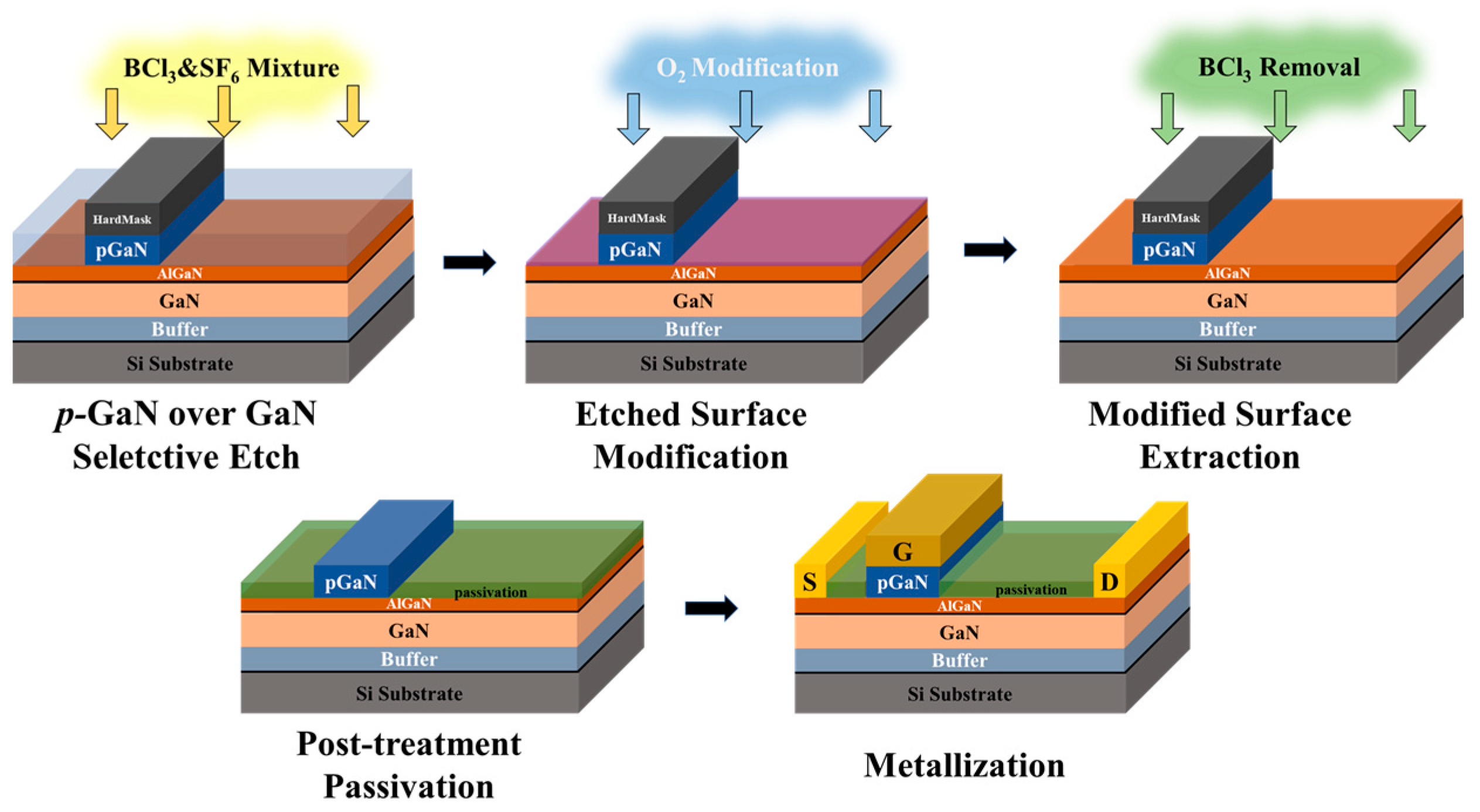
2. Device Structure and Fabrication
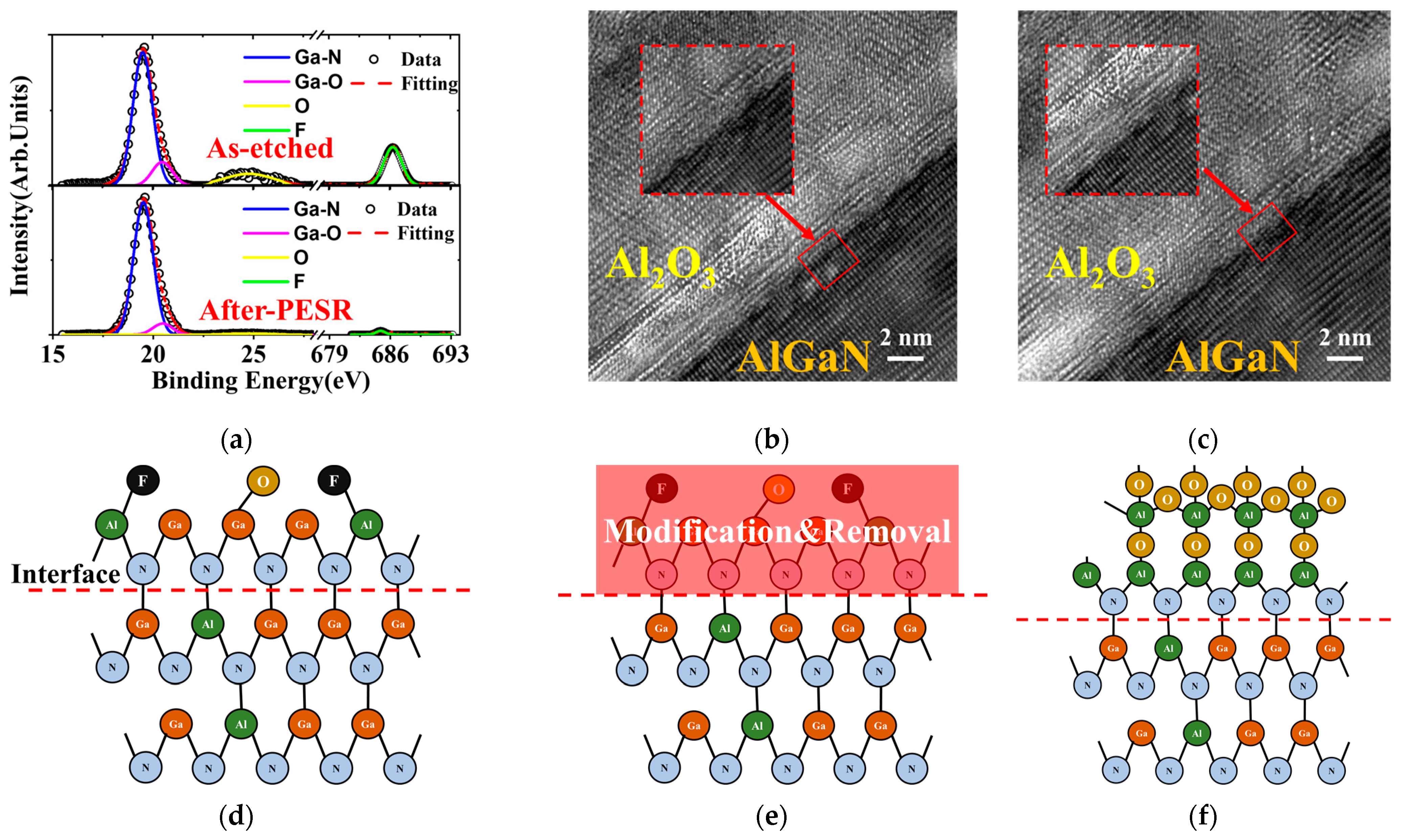
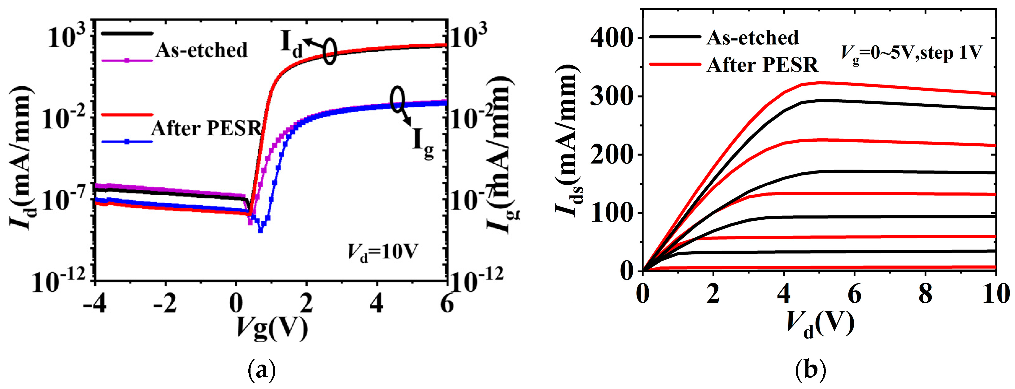
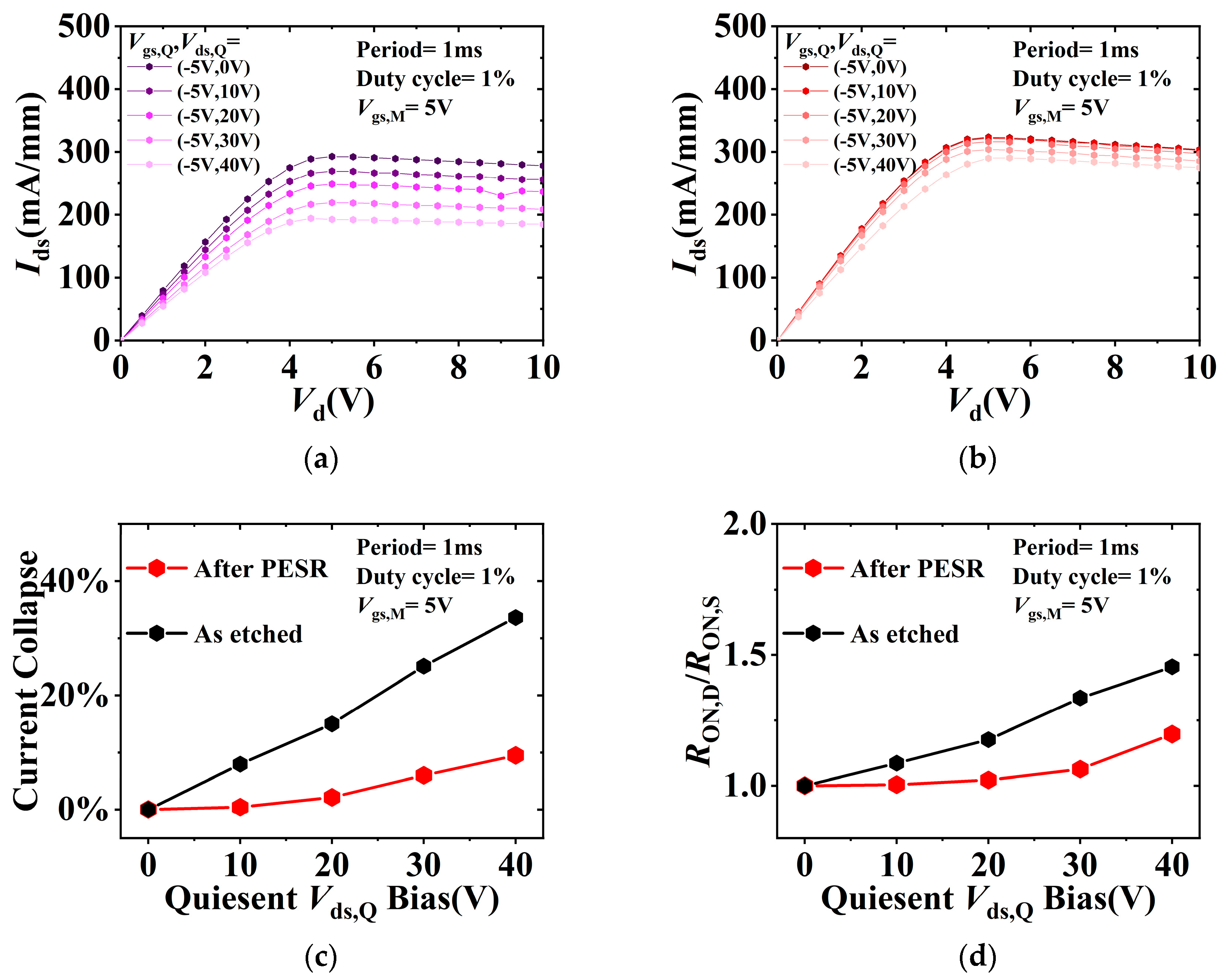
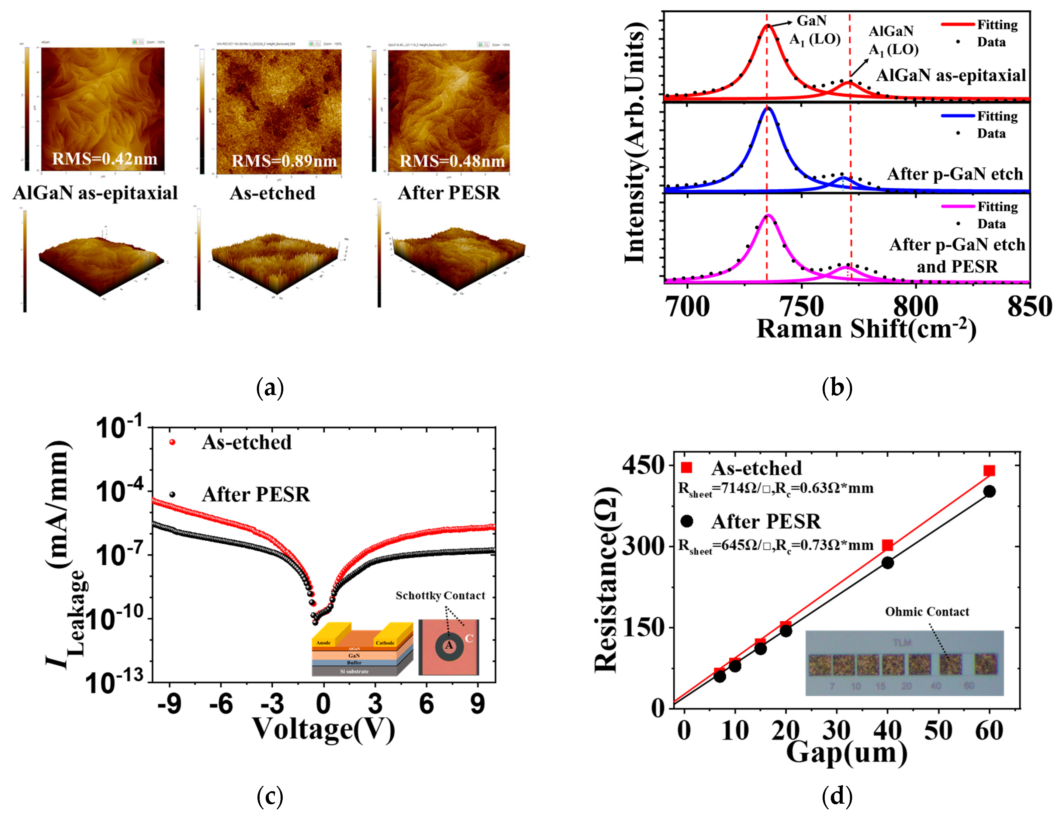
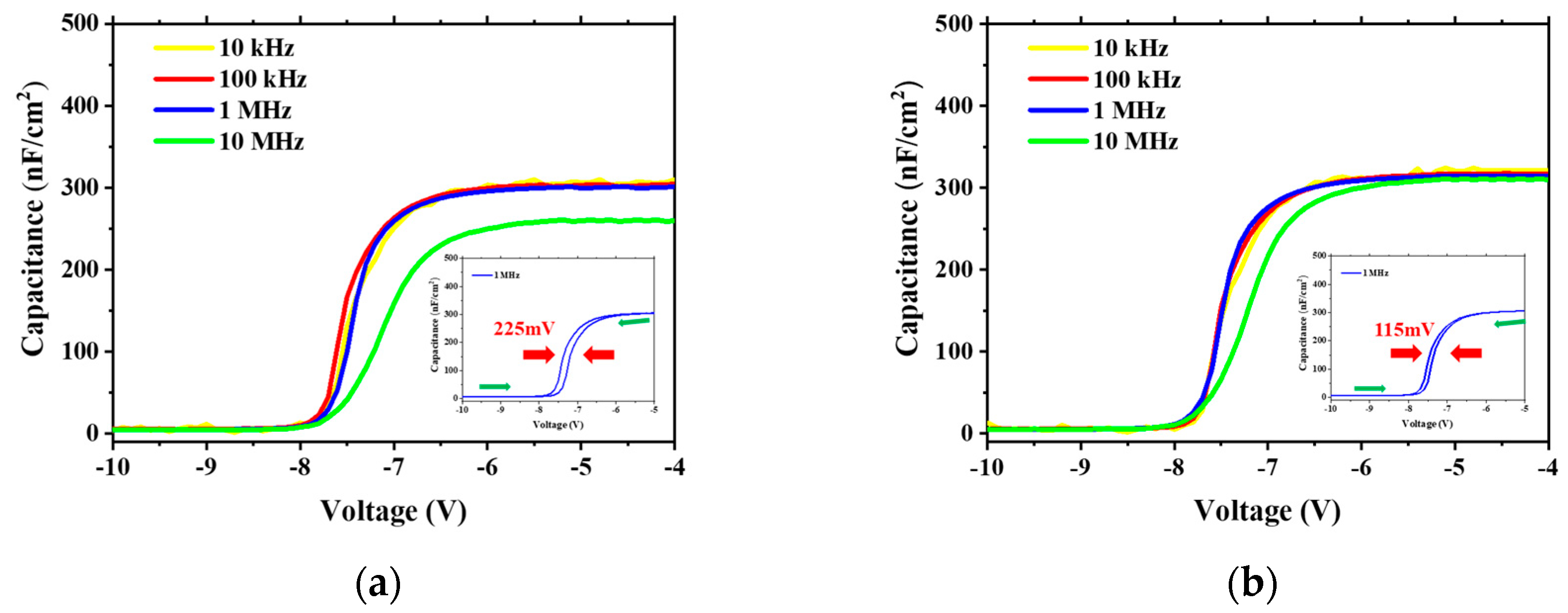
3. Results and Discussion
4. Conclusions
Author Contributions
Funding
Data Availability Statement
Conflicts of Interest
References
- Kumazaki, Y.; Uemura, K.; Sato, T.; Hashizume, T. Precise thickness control in recess etching of AlGaN/GaN hetero-structure using photocarrier-regulated electrochemical process. J. Appl. Phys. 2017, 121, 184501. [Google Scholar] [CrossRef]
- Millan, J.; Godignon, P.; Perpiñà, X.; Pérez-Tomás, A.; Rebollo, J. A Survey of Wide Bandgap Power Semiconductor Devices. IEEE Trans. Power Electron. 2014, 292, 2155–2163. [Google Scholar] [CrossRef]
- Jones, E.A.; Wang, F.F.; Costinett, D. Review of Commercial GaN Power Devices and GaN-Based Converter Design Challenges. IEEE J. Emerg. Sel. Top. Power Electron. 2016, 47, 707–719. [Google Scholar] [CrossRef]
- Wang, M.; Chen, K.J. Improvement of the Off-State Breakdown Voltage With Fluorine Ion Implantation in AlGaN/GaN HEMTs. IEEE Trans. Electron Devices 2011, 584, 460–465. [Google Scholar] [CrossRef]
- Oka, T.; Nozawa, T. AlGaN/GaN Recessed MIS-Gate HFET With High-Threshold-Voltage Normally-Off Operation for Power Electronics Applications. IEEE Electron Device Lett. 2008, 296, 68–670. [Google Scholar] [CrossRef]
- Hu, X.; Simin, G. Enhancement mode AlGaN/GaN HFET with selectively grown pn junction gate. Electron. Lett. 2000, 367, 53–754. [Google Scholar] [CrossRef]
- Fujii, T.; Tsuyukuchi, N.; Iwaya, M.; Kamiyama, S.; Amano, H.; Akasaki, I. High On/Off Ratio in Enhancement-Mode AlxGa1-xN/GaN Junction Heterostructure Field-Effect Transistors with P-Type GaN Gate Contact. Jpn. J. Appl. Phys. 2006, 45, L1048. [Google Scholar] [CrossRef]
- Uemoto, Y.; Hikita, M.; Ueno, H.; Matsuo, H.; Ishida, H.; Yanagihara, M.; Ueda, T.; Tanaka, T.; Ueda, D. Gate Injection Transistor (GIT)—A Normally-Off AlGaN/GaN Power Transistor Using Conductivity Modulation. IEEE Trans. Electron Devices 2007, 543, 3393–3399. [Google Scholar] [CrossRef]
- Ishida, M.; Ueda, T.; Tanaka, T.; Ueda, D. GaN on Si Technologies for Power Switching Devices. IEEE Trans. Electron Devices 2013, 603, 3053–3059. [Google Scholar] [CrossRef]
- Marcon, D.; Van Hove, M.; De Jaeger, B.; Posthuma, N.; Wellekens, D.; You, S.; Kang, X.; Wu, T.L.; Willems, M.; Stoffels, S.; et al. Direct comparison of GaN-based e-mode architectures (recessed MISHEMT and p-GaN HEMTs) processed on 200mm GaN-on-Si with Au-free technology. In Proceedings of the Proceedings of SPIE—The International Society for Optical Engineering, San Francisco, CA, USA, 13 March 2015; Volume 9363, Invited paper.
- Lükens, G.; Hahn, H.; Kalisch, H.; Vescan, A. Self-Aligned Process for Selectively Etched p-GaN-Gated AlGaN/GaN-on-Si HFETs. IEEE Trans. Electron Devices 2018, 65, 3732–3738. [Google Scholar] [CrossRef]
- Su, L.Y.; Lee, F.; Huang, J.J. Enhancement-Mode GaN-Based High-Electron Mobility Transistors on the Si Substrate with a P-Type GaN Cap Layer. IEEE Trans. Electron Devices 2014, 614, 460–465. [Google Scholar] [CrossRef]
- Zhang, P.; Wang, L.; Zhu, K.; Yang, Y.; Fan, R.; Pan, M.; Xu, S.; Xu, M.; Wang, C.; Wu, C.; et al. High Selectivity, Low Damage ICP Etching of p-GaN over AlGaN for Normally-off p-GaN HEMTs Application. Micromachines 2022, 13, 589. [Google Scholar] [CrossRef] [PubMed]
- Tereshchenko, O.E.; Shaibler, G.E.; Yaroshevich, A.S.; Shevelev, S.V.; Terekhov, A.S.; Lundin, V.V.; Zavarin, E.E.; Besyul’kin, A.I. Low-temperature method of cleaning p-GaN(0001) surfaces for photoemitters with effective negative electron affinity. Phys. Solid State 2004, 46, 1949–1953. [Google Scholar] [CrossRef]
- Buttari, D.; Chini, A.; Chakraborty, A.; McCarthy, L.; Xing, H.; Palacios, T.; Shen, L.; Keller, S.; Mishra, U.K. Selective dry etching of GaN over AlGaN in BCl3/SF6 mixtures. Int. J. High Speed Electron. Syst. 2004, 14, 756–761. [Google Scholar] [CrossRef]
- Liu, Y.; Chen, D.; Wei, G.; Lin, Z.; He, A.; Li, M.; Wang, P.; Zhang, R.; Zheng, Y. Temperature-dependent ultraviolet Raman scattering and anomalous Raman phenomenon of AlGaN/GaN heterostructure. Opt. Express 2019, 274, 4781–4788. [Google Scholar] [CrossRef] [PubMed]
- Reeves, G.K.; Harrison, H.B. Using TLM principles to determine MOSFET contact and parasitic resistance. Solid-State Electron. 1997, 411, 1067–1074. [Google Scholar] [CrossRef]
- Ramanan, N.; Lee, B.; Misra, V. Comparison of Methods for Accurate Characterization of Interface Traps in GaN MOS-HFET Devices. IEEE Trans. Electron Devices 2015, 625, 546–553. [Google Scholar] [CrossRef]
- Jin, D.; Alamo, J.A.D. Mechanisms responsible for dynamic ON-resistance in GaN high-voltage HEMTs. In Proceedings of the 24th International Symposium on Power Semiconductor Devices and ICs, Bruges, Belgium, 3–7 June 2012. [Google Scholar]


| Parameter | O2 Modification | BCl3 Removal |
|---|---|---|
| ICP power (W) | 400 | 200 |
| Bias power (W) | 0 | 6 |
| Chamber pressure (mTorr) | 10 | 10 |
| Gas flow rate (sccm) | 100 | 100 |
| Treatment time (s) | 15 | 5 |
Disclaimer/Publisher’s Note: The statements, opinions and data contained in all publications are solely those of the individual author(s) and contributor(s) and not of MDPI and/or the editor(s). MDPI and/or the editor(s) disclaim responsibility for any injury to people or property resulting from any ideas, methods, instructions or products referred to in the content. |
© 2023 by the authors. Licensee MDPI, Basel, Switzerland. This article is an open access article distributed under the terms and conditions of the Creative Commons Attribution (CC BY) license (https://creativecommons.org/licenses/by/4.0/).
Share and Cite
Wang, L.; Zhang, P.; Zhu, K.; Wang, Q.; Pan, M.; Sun, X.; Huang, Z.; Chen, K.; Yang, Y.; Xie, X.; et al. A Novel Atomic-Level Post-Etch-Surface-Reinforcement Process for High-Performance p-GaN Gate HEMTs Fabrication. Nanomaterials 2023, 13, 2275. https://doi.org/10.3390/nano13162275
Wang L, Zhang P, Zhu K, Wang Q, Pan M, Sun X, Huang Z, Chen K, Yang Y, Xie X, et al. A Novel Atomic-Level Post-Etch-Surface-Reinforcement Process for High-Performance p-GaN Gate HEMTs Fabrication. Nanomaterials. 2023; 13(16):2275. https://doi.org/10.3390/nano13162275
Chicago/Turabian StyleWang, Luyu, Penghao Zhang, Kaiyue Zhu, Qiang Wang, Maolin Pan, Xin Sun, Ziqiang Huang, Kun Chen, Yannan Yang, Xinling Xie, and et al. 2023. "A Novel Atomic-Level Post-Etch-Surface-Reinforcement Process for High-Performance p-GaN Gate HEMTs Fabrication" Nanomaterials 13, no. 16: 2275. https://doi.org/10.3390/nano13162275
APA StyleWang, L., Zhang, P., Zhu, K., Wang, Q., Pan, M., Sun, X., Huang, Z., Chen, K., Yang, Y., Xie, X., Huang, H., Hu, X., Xu, S., Wu, C., Wang, C., Xu, M., & Zhang, D. W. (2023). A Novel Atomic-Level Post-Etch-Surface-Reinforcement Process for High-Performance p-GaN Gate HEMTs Fabrication. Nanomaterials, 13(16), 2275. https://doi.org/10.3390/nano13162275