
Evolution of Mn1−xGexBi2Te4 Electronic Structure under Variation of Ge Content

 , , , , , , , , and
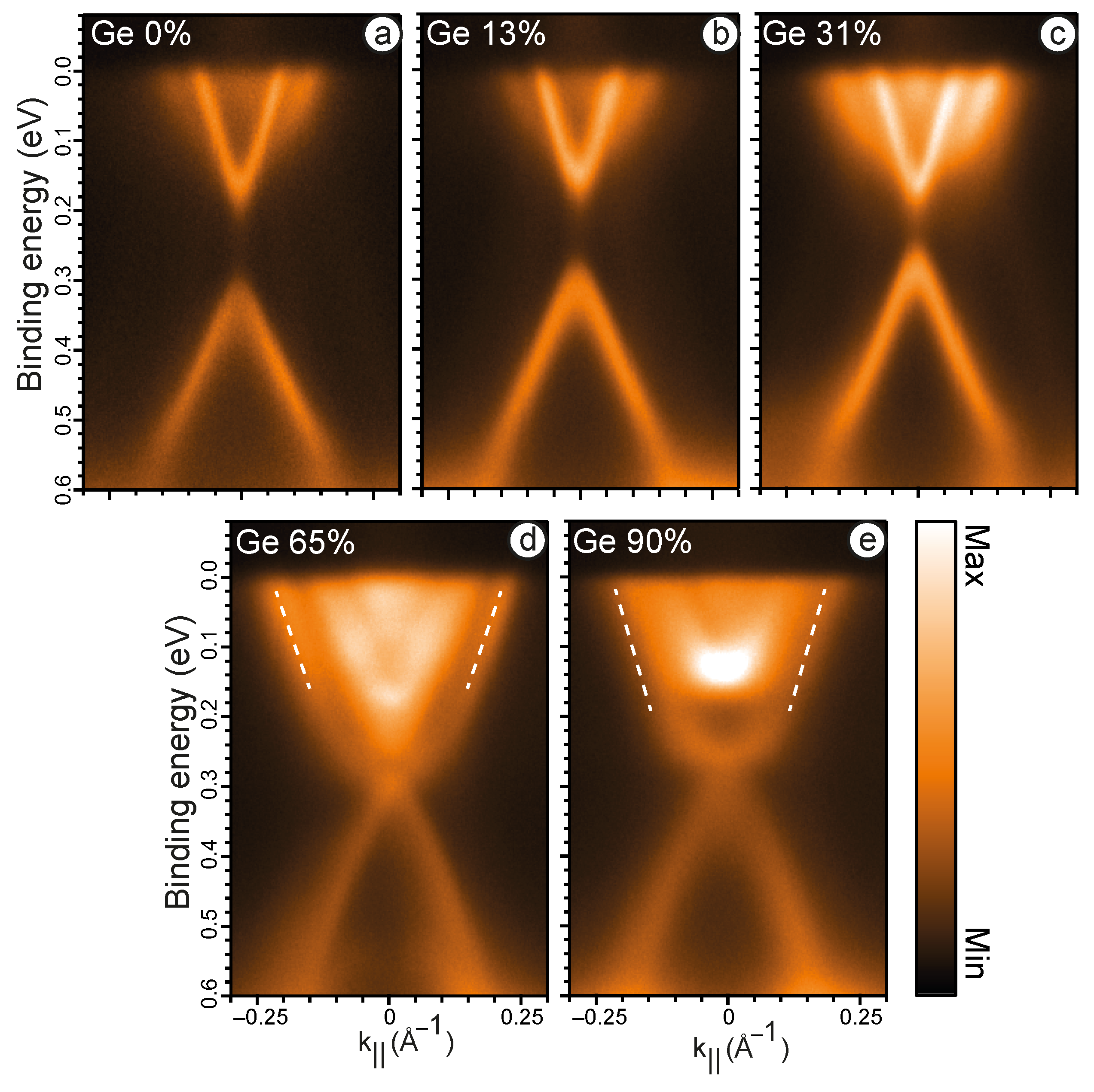
Abstract
1. Introduction
2. Materials and Methods
3. Results and Discussion
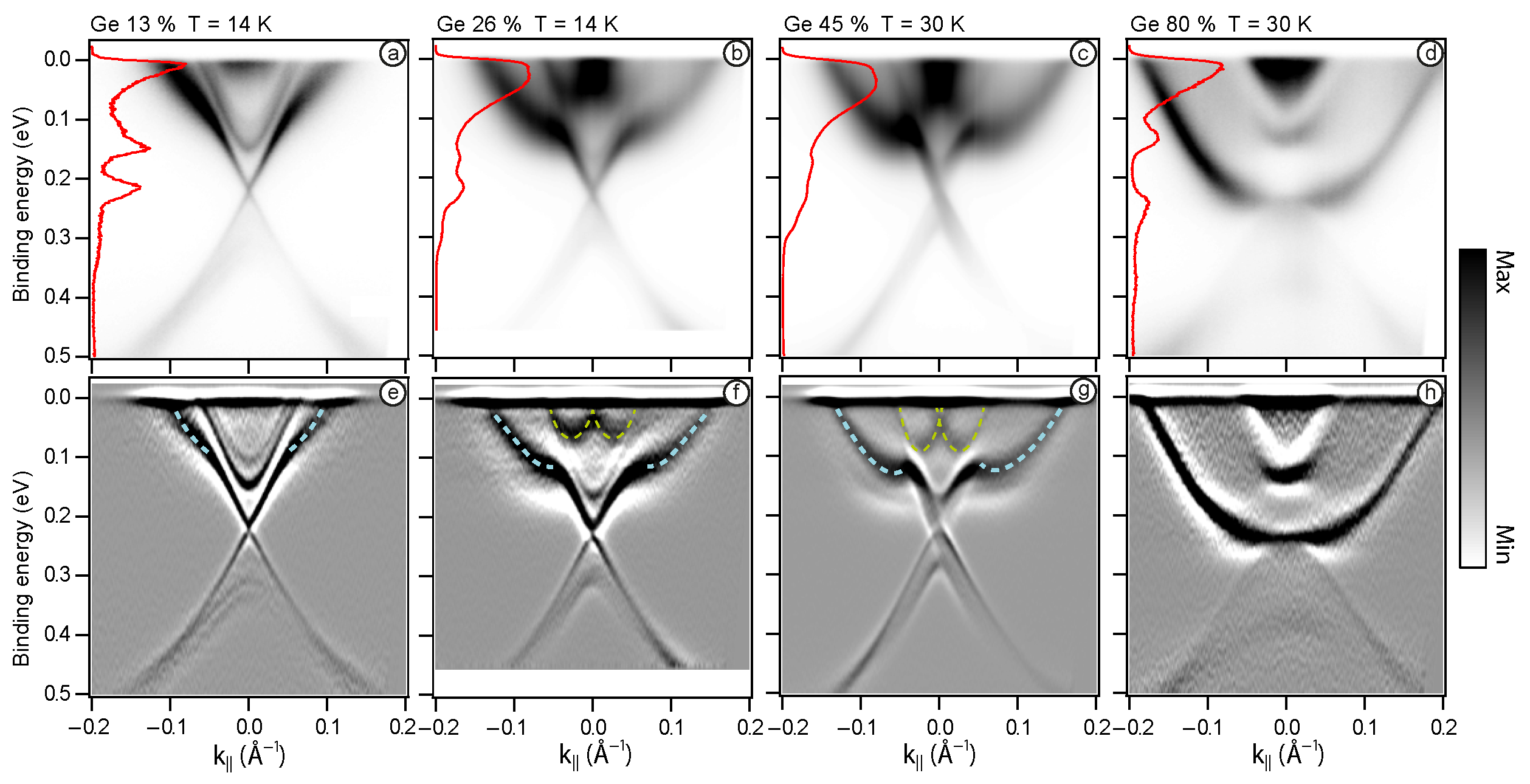
3.1. Experimental Results
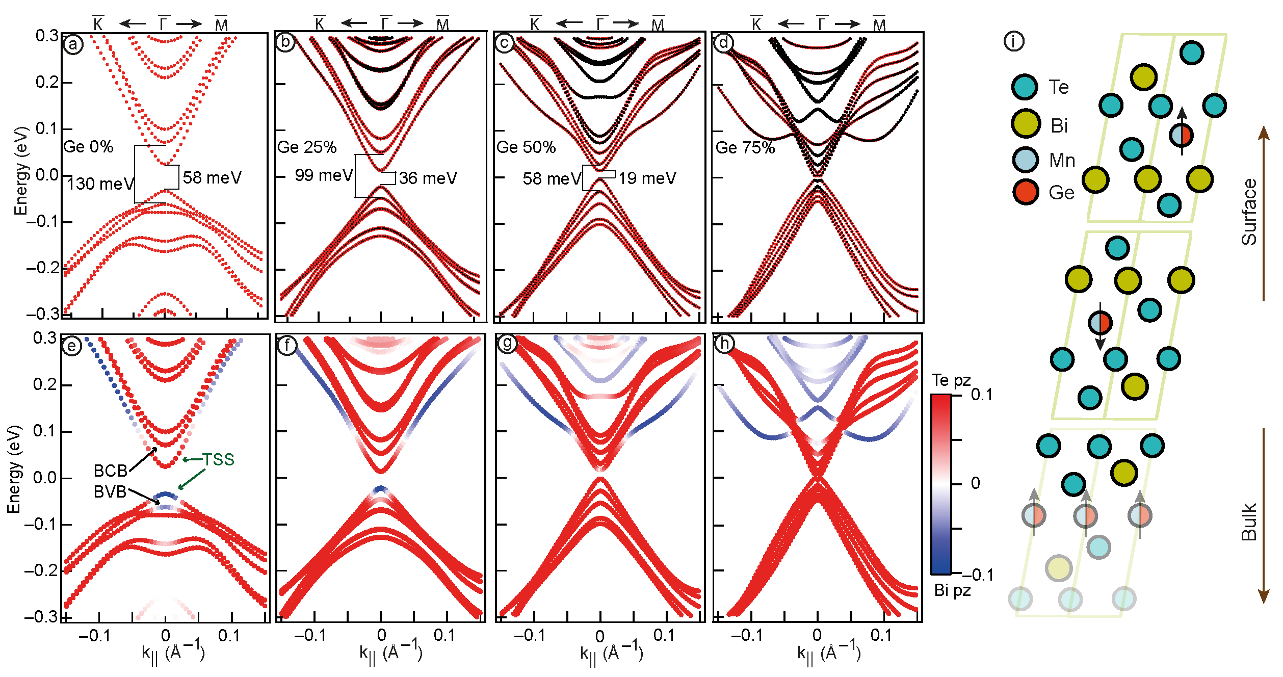
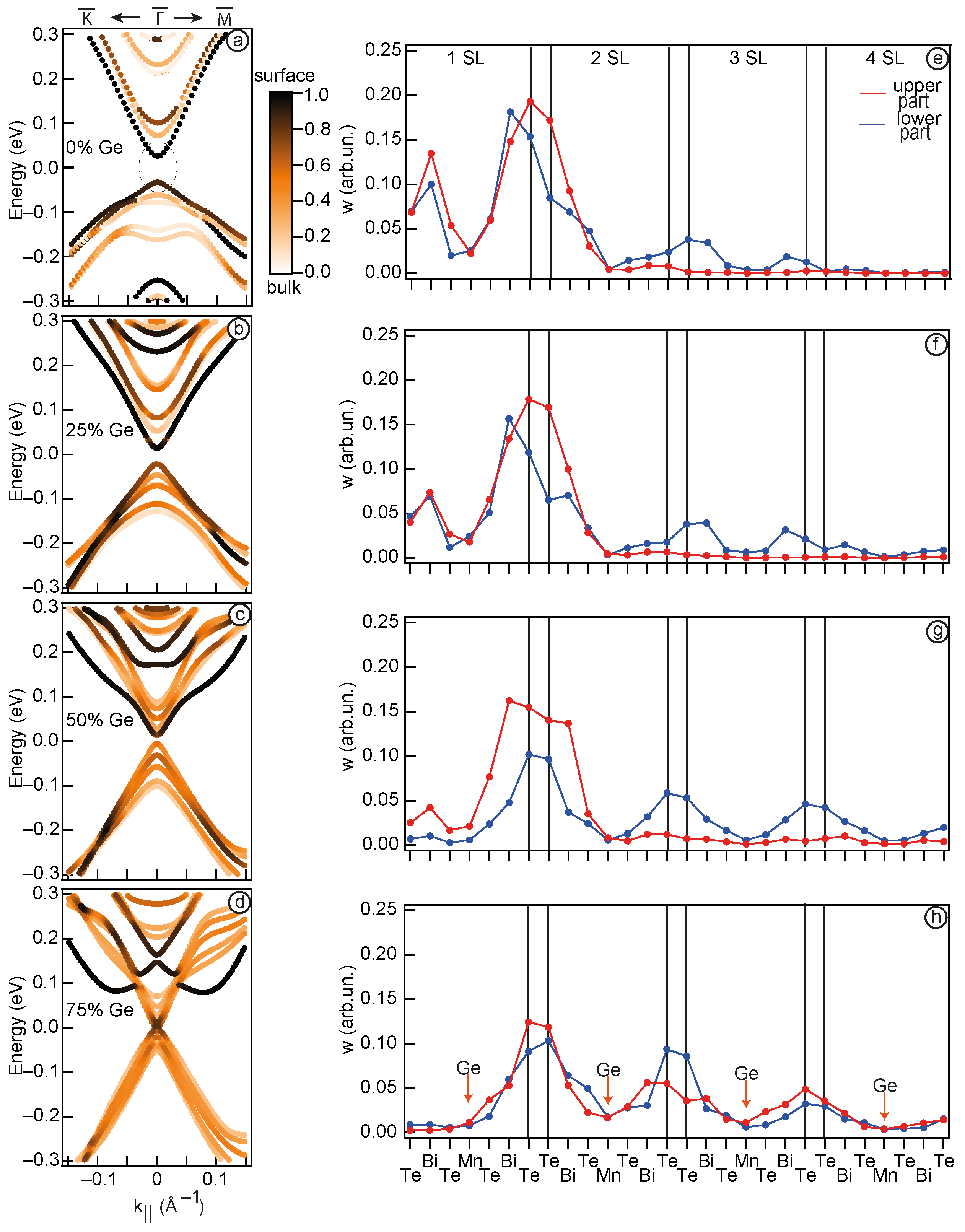
3.2. Theoretical Calculations
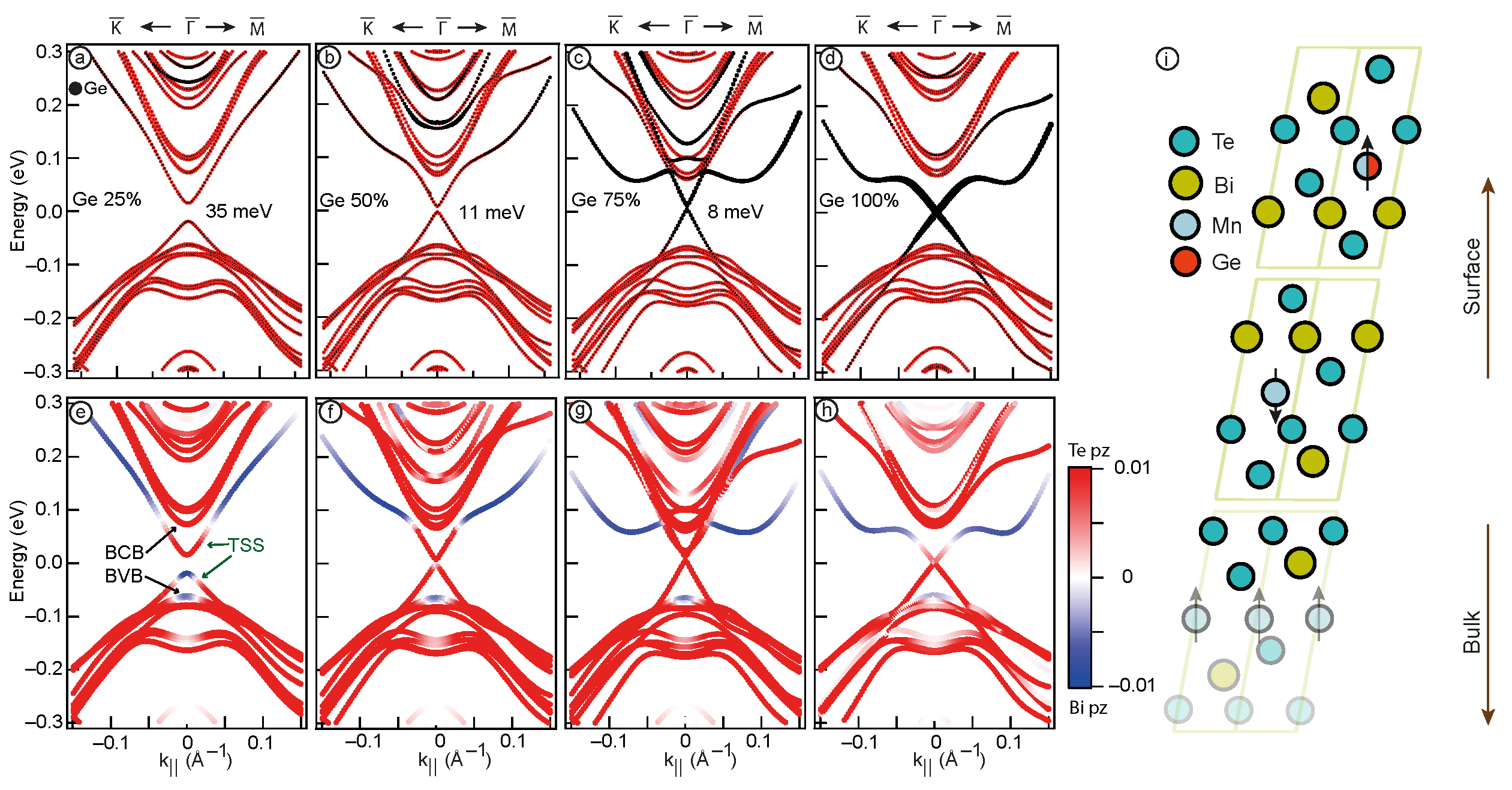
3.2.1. Bulk Mn/Ge Substitution
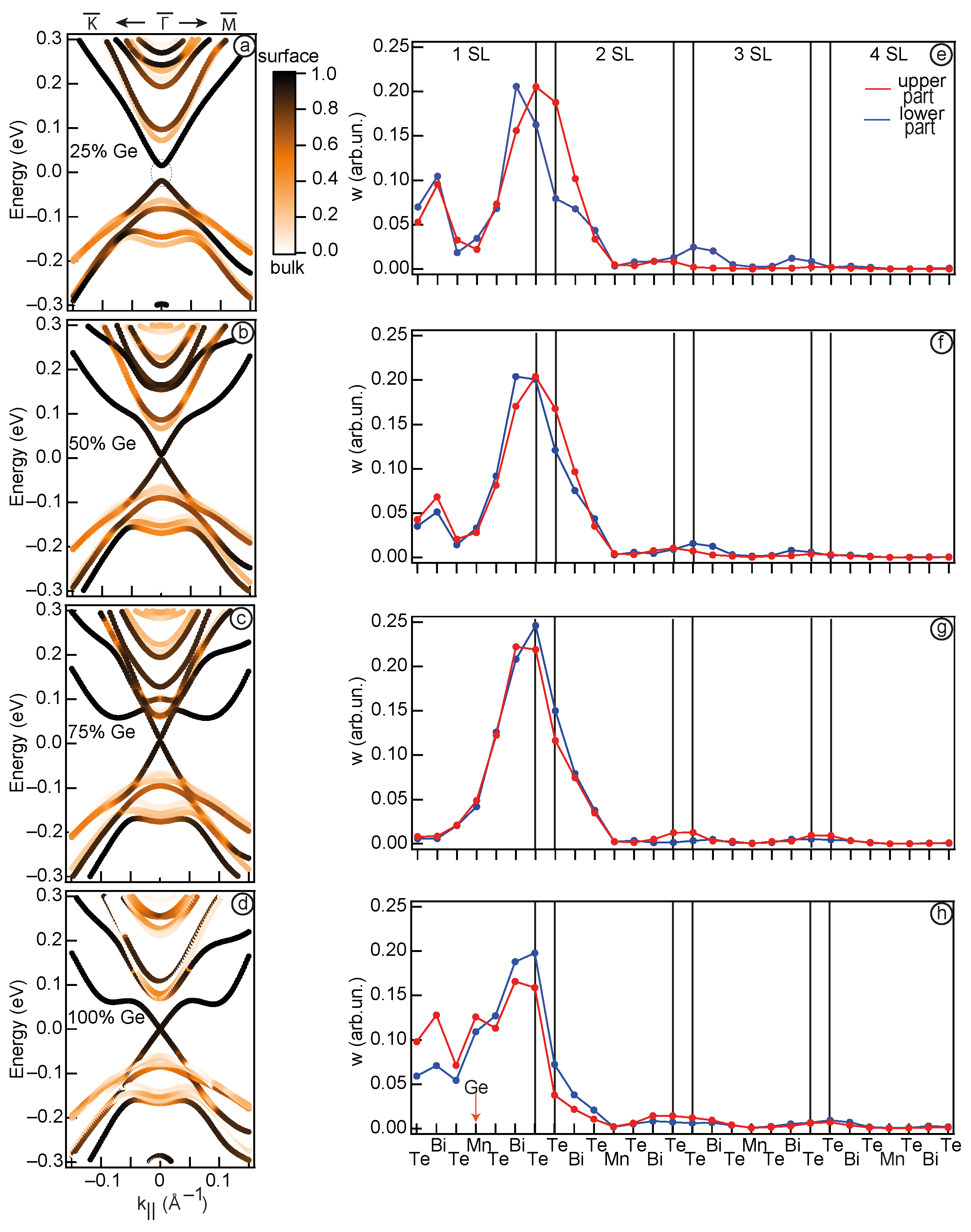
3.2.2. Surface Mn/Ge Substitution
4. Conclusions
Author Contributions
Funding
Data Availability Statement
Acknowledgments
Conflicts of Interest
References
- Hasan, M.Z.; Kane, C.L. Colloquium: Topological insulators. Rev. Mod. Phys. 2010, 82, 3045. [Google Scholar] [CrossRef]
- Qi, X.L.; Hughes, T.L.; Zhang, S.C. Topological field theory of time-reversal invariant insulators. Phys. Rev. B 2008, 78, 195424. [Google Scholar] [CrossRef]
- Qi, X.L.; Zhang, S.C. Topological insulators and superconductors. Rev. Mod. Phys. 2011, 83, 1057. [Google Scholar] [CrossRef]
- Chen, Y.P. Topological insulator-based energy efficient devices. In Proceedings of the Micro-and Nanotechnology Sensors, Systems, and Applications IV, Baltimore, MD, USA, 23–27 April 2012; Volume 8373, pp. 94–98. [Google Scholar]
- Wang, J.; DaSilva, A.M.; Chang, C.Z.; He, K.; Jain, J.; Samarth, N.; Ma, X.C.; Xue, Q.K.; Chan, M.H. Evidence for electron-electron interaction in topological insulator thin films. Phys. Rev. B 2011, 83, 245438. [Google Scholar] [CrossRef]
- Tokura, Y.; Yasuda, K.; Tsukazaki, A. Magnetic topological insulators. Nat. Rev. Phys. 2019, 1, 126–143. [Google Scholar] [CrossRef]
- Chang, C.Z.; Zhang, J.; Feng, X.; Shen, J.; Zhang, Z.; Guo, M.; Li, K.; Ou, Y.; Wei, P.; Wang, L.L.; et al. Experimental observation of the quantum anomalous Hall effect in a magnetic topological insulator. Science 2013, 340, 167–170. [Google Scholar] [CrossRef]
- He, Q.L.; Pan, L.; Stern, A.L.; Burks, E.C.; Che, X.; Yin, G.; Wang, J.; Lian, B.; Zhou, Q.; Choi, E.S.; et al. Chiral Majorana fermion modes in a quantum anomalous Hall insulator–superconductor structure. Science 2017, 357, 294–299. [Google Scholar] [CrossRef]
- Otrokov, M.M.; Klimovskikh, I.I.; Bentmann, H.; Estyunin, D.; Zeugner, A.; Aliev, Z.S.; Gaß, S.; Wolter, A.; Koroleva, A.; Shikin, A.M.; et al. Prediction and observation of an antiferromagnetic topological insulator. Nature 2019, 576, 416–422. [Google Scholar] [CrossRef]
- Li, J.; Li, Y.; Du, S.; Wang, Z.; Gu, B.L.; Zhang, S.C.; He, K.; Duan, W.; Xu, Y. Intrinsic magnetic topological insulators in van der Waals layered MnBi2Te4-family materials. Sci. Adv. 2019, 5, eaaw5685. [Google Scholar] [CrossRef]
- Shikin, A.; Makarova, T.; Eryzhenkov, A.; Usachov, D.Y.; Estyunin, D.; Glazkova, D.; Klimovskikh, I.; Rybkin, A.; Tarasov, A. Routes for the topological surface state energy gap modulation in antiferromagnetic MnBi2Te4. Phys. B Condens. Matter 2023, 649, 414443. [Google Scholar] [CrossRef]
- Shikin, A.; Zaitsev, N.; Tarasov, A.; Makarova, T.; Glazkova, D.; Estyunin, D.; Klimovskikh, I. Electronic and Spin Structure of Topological Surface States in MnBi4Te7 and MnBi6Te10 and Their Modification by an Applied Electric Field. JETP Lett. 2022, 116, 556–566. [Google Scholar] [CrossRef]
- Shikin, A.M.; Estyunin, D.; Zaitsev, N.L.; Glazkova, D.; Klimovskikh, I.I.; Filnov, S.; Rybkin, A.G.; Schwier, E.; Kumar, S.; Kimura, A.; et al. Sample-dependent Dirac-point gap in MnBi2Te4 and its response to applied surface charge: A combined photoemission and ab-initio study. Phys. Rev. B 2021, 104, 115168. [Google Scholar] [CrossRef]
- Eremeev, S.; Vergniory, M.; Menshchikova, T.V.; Shaposhnikov, A.; Chulkov, E.V. The effect of van der Waal’s gap expansions on the surface electronic structure of layered topological insulators. New J. Phys. 2012, 14, 113030. [Google Scholar] [CrossRef]
- Shikin, A.M.; Estyunin, D.; Klimovskikh, I.I.; Filnov, S.; Schwier, E.; Kumar, S.; Miyamoto, K.; Okuda, T.; Kimura, A.; Kuroda, K.; et al. Nature of the Dirac gap modulation and surface magnetic interaction in axion antiferromagnetic topological insulator MnBi2Te4. Sci. Rep. 2020, 10, 13226. [Google Scholar] [CrossRef]
- Makarova, T.; Shikin, A.; Eryzhenkov, A.; Tarasov, A. Influence of Structural Parameters on the Electronic Structure of Topological Surface States in MnBi2Te4. J. Exp. Theor. Phys. 2023, 136, 630–637. [Google Scholar] [CrossRef]
- Qi, X.L.; Zhang, S.C. The quantum spin Hall effect and topological insulators. arXiv 2010, arXiv:1001.1602. [Google Scholar] [CrossRef]
- Li, Y.; Huang, C.; Wang, G.; Hu, J.; Duan, S.; Xu, C.; Lu, Q.; Jing, Q.; Zhang, W.; Qian, D. Topological Dirac surface states in ternary compounds GeBi2Te4, SnBi2Te4 and Sn0.571Bi2.286Se4. Chin. Phys. B 2021, 30, 127901. [Google Scholar] [CrossRef]
- Tarasov, A.V.; Makarova, T.P.; Estyunin, D.A.; Eryzhenkov, A.V.; Klimovskikh, I.I.; Golyashov, V.A.; Kokh, K.A.; Tereshchenko, O.E.; Shikin, A.M. Topological Phase Transitions Driven by Sn Doping in (Mn1−xSnx) Bi2Te4. Symmetry 2023, 15, 469. [Google Scholar] [CrossRef]
- Kuroda, K.; Miyahara, H.; Ye, M.; Eremeev, S.; Koroteev, Y.M.; Krasovskii, E.; Chulkov, E.; Hiramoto, S.; Moriyoshi, C.; Kuroiwa, Y.; et al. Experimental verification of PbBi2Te4 as a 3D topological insulator. Phys. Rev. Lett. 2012, 108, 206803. [Google Scholar] [CrossRef]
- Arita, M.; Sato, H.; Shimada, K.; Namatame, H.; Taniguchi, M.; Sasaki, M.; Kitaura, M.; Ohnishi, A.; Kim, H.J. Angle resolved photoemission study of GeBi2Te4. In Proceedings of the 12th Asia Pacific Physics Conference (APPC12), Makuhari Messe, Japan, 14–19 July 2013; p. 012017. [Google Scholar]
- Okamoto, K.; Kuroda, K.; Miyahara, H.; Miyamoto, K.; Okuda, T.; Aliev, Z.; Babanly, M.; Amiraslanov, I.; Shimada, K.; Namatame, H.; et al. Observation of a highly spin-polarized topological surface state in GeBi2Te4. Phys. Rev. B 2012, 86, 195304. [Google Scholar] [CrossRef]
- Qian, T.; Yao, Y.T.; Hu, C.; Feng, E.; Cao, H.; Mazin, I.I.; Chang, T.R.; Ni, N. Magnetic dilution effect and topological phase transitions in (Mn1−x Pbx)Bi2Te4. Phys. Rev. B 2022, 106, 045121. [Google Scholar] [CrossRef]
- Zhu, J.; Naveed, M.; Chen, B.; Du, Y.; Guo, J.; Xie, H.; Fei, F. Magnetic and electrical transport study of the antiferromagnetic topological insulator Sn-doped MnBi2Te4. Phys. Rev. B 2021, 103, 144407. [Google Scholar] [CrossRef]
- Changdar, S.; Ghosh, S.; Vijay, K.; Kar, I.; Routh, S.; Maheshwari, P.; Ghorai, S.; Banik, S.; Thirupathaiah, S. Nonmagnetic Sn doping effect on the electronic and magnetic properties of antiferromagnetic topological insulator MnBi2Te4. Phys. B Condens. Matter 2023, 657, 414799. [Google Scholar] [CrossRef]
- Yan, J. The elusive quantum anomalous Hall effect in MnBi2Te4: A materials perspective. arXiv 2021, arXiv:2112.09070. [Google Scholar] [CrossRef]
- Frolov, A.; Usachov, D.; Tarasov, A.; Fedorov, A.; Bokai, K.; Klimovskikh, I.; Stolyarov, V.; Sergeev, A.; Lavrov, A.; Golyashov, V.; et al. Magnetic Dirac semimetal state of (Mn,Ge)Bi2Te4. arXiv 2023, arXiv:2306.13024. [Google Scholar]
- Neupane, M.; Xu, S.Y.; Wray, L.A.; Petersen, A.; Shankar, R.; Alidoust, N.; Liu, C.; Fedorov, A.; Ji, H.; Allred, J.M.; et al. Topological surface states and Dirac point tuning in ternary topological insulators. Phys. Rev. B 2012, 85, 235406. [Google Scholar] [CrossRef]
- Iwasawa, H.; Schwier, E.F.; Arita, M.; Ino, A.; Namatame, H.; Taniguchi, M.; Aiura, Y.; Shimada, K. Development of laser-based scanning μ-ARPES system with ultimate energy and momentum resolutions. Ultramicroscopy 2017, 182, 85–91. [Google Scholar] [CrossRef]
- Iwasawa, H.; Takita, H.; Goto, K.; Mansuer, W.; Miyashita, T.; Schwier, E.F.; Ino, A.; Shimada, K.; Aiura, Y. Accurate and efficient data acquisition methods for high-resolution angle-resolved photoemission microscopy. Sci. Rep. 2018, 8, 17431. [Google Scholar] [CrossRef]
- Ozaki, T. Variationally optimized atomic orbitals for large-scale electronic structures. Phys. Rev. B 2003, 67, 155108. [Google Scholar] [CrossRef]
- Ozaki, T.; Kino, H. Numerical atomic basis orbitals from H to Kr. Phys. Rev. B 2004, 69, 195113. [Google Scholar] [CrossRef]
- Ozaki, T.; Kino, H. Efficient projector expansion for the ab-initio LCAO method. Phys. Rev. B 2005, 72, 045121. [Google Scholar] [CrossRef]
- Troullier, N.; Martins, J.L. Efficient pseudopotentials for plane-wave calculations. II. Operators for fast iterative diagonalization. Phys. Rev. B 1991, 43, 8861. [Google Scholar] [CrossRef] [PubMed]
- Perdew, J.P.; Burke, K.; Ernzerhof, M. Generalized gradient approximation made simple. Phys. Rev. Lett. 1996, 77, 3865. [Google Scholar] [CrossRef]
- Vidal, R.; Bentmann, H.; Peixoto, T.; Zeugner, A.; Moser, S.; Min, C.H.; Schatz, S.; Kißner, K.; Ünzelmann, M.; Fornari, C.; et al. Surface states and Rashba-type spin polarization in antiferromagnetic MnBi2Te4 (0001). Phys. Rev. B 2019, 100, 121104. [Google Scholar] [CrossRef]
- Chen, Y.; Xu, L.; Li, J.; Li, Y.; Wang, H.; Zhang, C.; Li, H.; Wu, Y.; Liang, A.; Chen, C.; et al. Topological electronic structure and its temperature evolution in antiferromagnetic topological insulator MnBi2Te4. Phys. Rev. X 2019, 9, 041040. [Google Scholar] [CrossRef]
- Ma, X.M.; Zhao, Y.; Zhang, K.; Kumar, S.; Lu, R.; Li, J.; Yao, Q.; Shao, J.; Hou, F.; Wu, X.; et al. Realization of a tunable surface Dirac gap in Sb-doped MnBi2Te4. Phys. Rev. B 2021, 103, L121112. [Google Scholar] [CrossRef]
- Nevola, D.; Li, H.X.; Yan, J.Q.; Moore, R.; Lee, H.N.; Miao, H.; Johnson, P.D. Coexistence of surface ferromagnetism and a gapless topological state in MnBi2Te4. Phys. Rev. Lett. 2020, 125, 117205. [Google Scholar] [CrossRef]
- Estyunin, D.; Klimovskikh, I.I.; Shikin, A.M.; Schwier, E.; Otrokov, M.; Kimura, A.; Kumar, S.; Filnov, S.; Aliev, Z.S.; Babanly, M.; et al. Signatures of temperature driven antiferromagnetic transition in the electronic structure of topological insulator MnBi2Te4. APL Mater. 2020, 8, 021105. [Google Scholar] [CrossRef]
- Garnica, M.; Otrokov, M.M.; Aguilar, P.C.; Klimovskikh, I.I.; Estyunin, D.; Aliev, Z.S.; Amiraslanov, I.R.; Abdullayev, N.A.; Zverev, V.N.; Babanly, M.B.; et al. Native point defects and their implications for the Dirac point gap at MnBi2Te4 (0001). npj Quantum Mater. 2022, 7, 7. [Google Scholar] [CrossRef]
- Otrokov, M.; Rusinov, I.P.; Blanco-Rey, M.; Hoffmann, M.; Vyazovskaya, A.Y.; Eremeev, S.; Ernst, A.; Echenique, P.M.; Arnau, A.; Chulkov, E.V. Unique thickness-dependent properties of the van der Waals interlayer antiferromagnet MnBi2Te4 films. Phys. Rev. Lett. 2019, 122, 107202. [Google Scholar] [CrossRef]
- Li, Y.; Jiang, Y.; Zhang, J.; Liu, Z.; Yang, Z.; Wang, J. Intrinsic topological phases in Mn2Bi2Te5 tuned by the layer magnetization. Phys. Rev. B 2020, 102, 121107. [Google Scholar] [CrossRef]
- Zhu, T.; Wang, H.; Zhang, H.; Xing, D. Tunable dynamical magnetoelectric effect in antiferromagnetic topological insulator MnBi2Te4 films. npj Comput. Mater. 2021, 7, 121. [Google Scholar] [CrossRef]
- Liang, A.; Chen, C.; Zheng, H.; Xia, W.; Huang, K.; Wei, L.; Yang, H.; Chen, Y.; Zhang, X.; Xu, X.; et al. Approaching a Minimal Topological Electronic Structure in Antiferromagnetic Topological Insulator MnBi2Te4 via Surface Modification. Nano Lett. 2022, 22, 4307–4314. [Google Scholar] [CrossRef] [PubMed]
- Fukasawa, T.; Kusaka, S.; Sumida, K.; Hashizume, M.; Ichinokura, S.; Takeda, Y.; Ideta, S.; Tanaka, K.; Shimizu, R.; Hitosugi, T.; et al. Absence of ferromagnetism in MnBi2Te4/Bi2Te3 down to 6 K. Phys. Rev. B 2021, 103, 205405. [Google Scholar] [CrossRef]
- Kagerer, P.; Fornari, C.; Buchberger, S.; Tschirner, T.; Veyrat, L.; Kamp, M.; Tcakaev, A.; Zabolotnyy, V.; Morelhão, S.; Geldiyev, B.; et al. Two-dimensional ferromagnetic extension of a topological insulator. Phys. Rev. Res. 2023, 5, L022019. [Google Scholar] [CrossRef]
- Hirahara, T.; Eremeev, S.V.; Shirasawa, T.; Okuyama, Y.; Kubo, T.; Nakanishi, R.; Akiyama, R.; Takayama, A.; Hajiri, T.; Ideta, S.-i.; et al. Large-gap magnetic topological heterostructure formed by subsurface incorporation of a ferromagnetic layer. Nano Lett. 2017, 17, 3493–3500. [Google Scholar] [CrossRef]
- Hirahara, T.; Otrokov, M.M.; Sasaki, T.; Sumida, K.; Tomohiro, Y.; Kusaka, S.; Okuyama, Y.; Ichinokura, S.; Kobayashi, M.; Takeda, Y.; et al. Fabrication of a novel magnetic topological heterostructure and temperature evolution of its massive Dirac cone. Nat. Commun. 2020, 11, 4821. [Google Scholar] [CrossRef]


Disclaimer/Publisher’s Note: The statements, opinions and data contained in all publications are solely those of the individual author(s) and contributor(s) and not of MDPI and/or the editor(s). MDPI and/or the editor(s) disclaim responsibility for any injury to people or property resulting from any ideas, methods, instructions or products referred to in the content. |
© 2023 by the authors. Licensee MDPI, Basel, Switzerland. This article is an open access article distributed under the terms and conditions of the Creative Commons Attribution (CC BY) license (https://creativecommons.org/licenses/by/4.0/).
Share and Cite
Estyunina, T.P.; Shikin, A.M.; Estyunin, D.A.; Eryzhenkov, A.V.; Klimovskikh, I.I.; Bokai, K.A.; Golyashov, V.A.; Kokh, K.A.; Tereshchenko, O.E.; Kumar, S.; et al. Evolution of Mn1−xGexBi2Te4 Electronic Structure under Variation of Ge Content. Nanomaterials 2023, 13, 2151. https://doi.org/10.3390/nano13142151
Estyunina TP, Shikin AM, Estyunin DA, Eryzhenkov AV, Klimovskikh II, Bokai KA, Golyashov VA, Kokh KA, Tereshchenko OE, Kumar S, et al. Evolution of Mn1−xGexBi2Te4 Electronic Structure under Variation of Ge Content. Nanomaterials. 2023; 13(14):2151. https://doi.org/10.3390/nano13142151
Chicago/Turabian StyleEstyunina, Tatiana P., Alexander M. Shikin, Dmitry A. Estyunin, Alexander V. Eryzhenkov, Ilya I. Klimovskikh, Kirill A. Bokai, Vladimir A. Golyashov, Konstantin A. Kokh, Oleg E. Tereshchenko, Shiv Kumar, and et al. 2023. "Evolution of Mn1−xGexBi2Te4 Electronic Structure under Variation of Ge Content" Nanomaterials 13, no. 14: 2151. https://doi.org/10.3390/nano13142151
APA StyleEstyunina, T. P., Shikin, A. M., Estyunin, D. A., Eryzhenkov, A. V., Klimovskikh, I. I., Bokai, K. A., Golyashov, V. A., Kokh, K. A., Tereshchenko, O. E., Kumar, S., Shimada, K., & Tarasov, A. V. (2023). Evolution of Mn1−xGexBi2Te4 Electronic Structure under Variation of Ge Content. Nanomaterials, 13(14), 2151. https://doi.org/10.3390/nano13142151