
Colloidal 2D Lead Chalcogenide Nanocrystals: Synthetic Strategies, Optical Properties, and Applications


Abstract
:1. Introduction
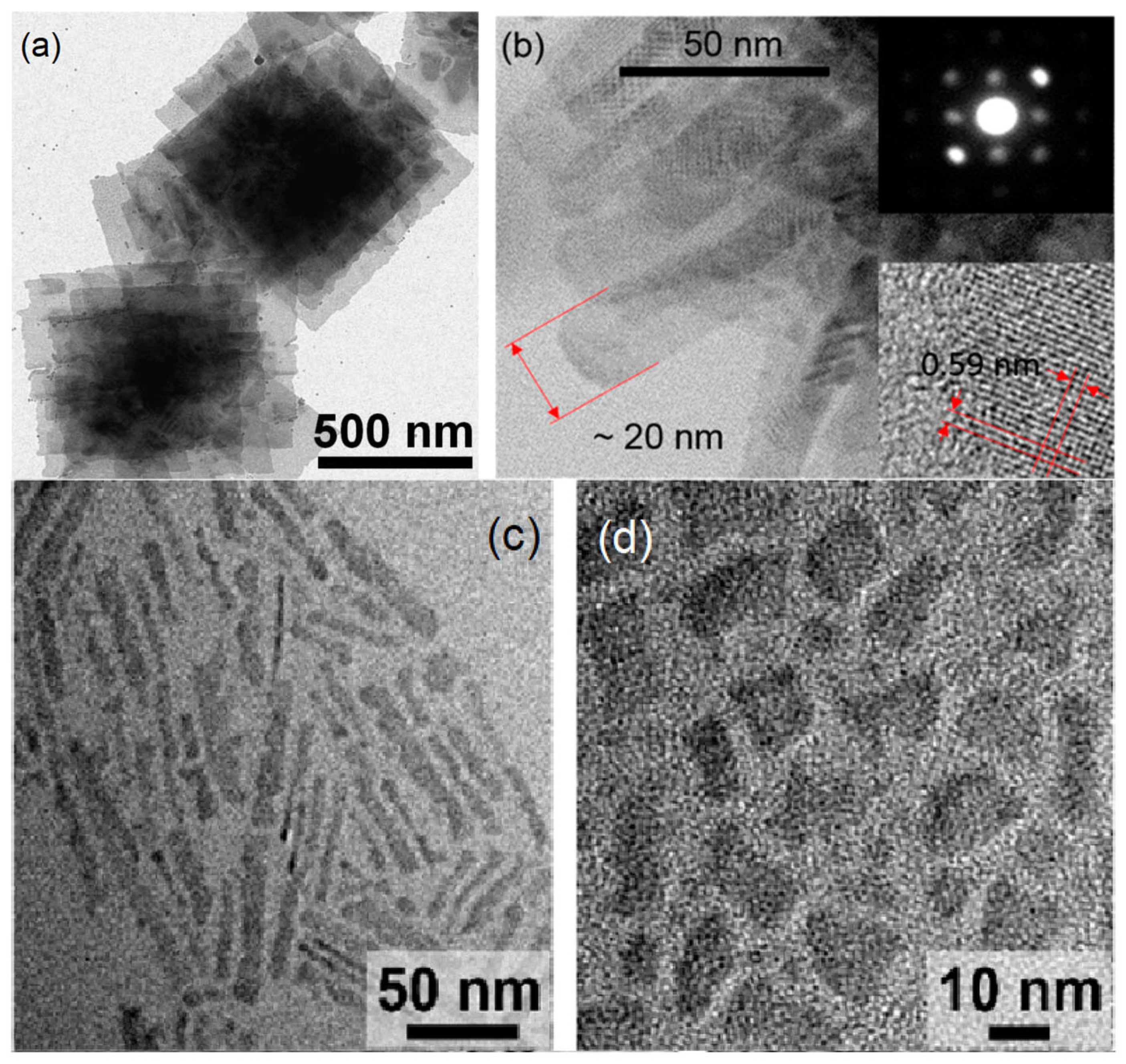
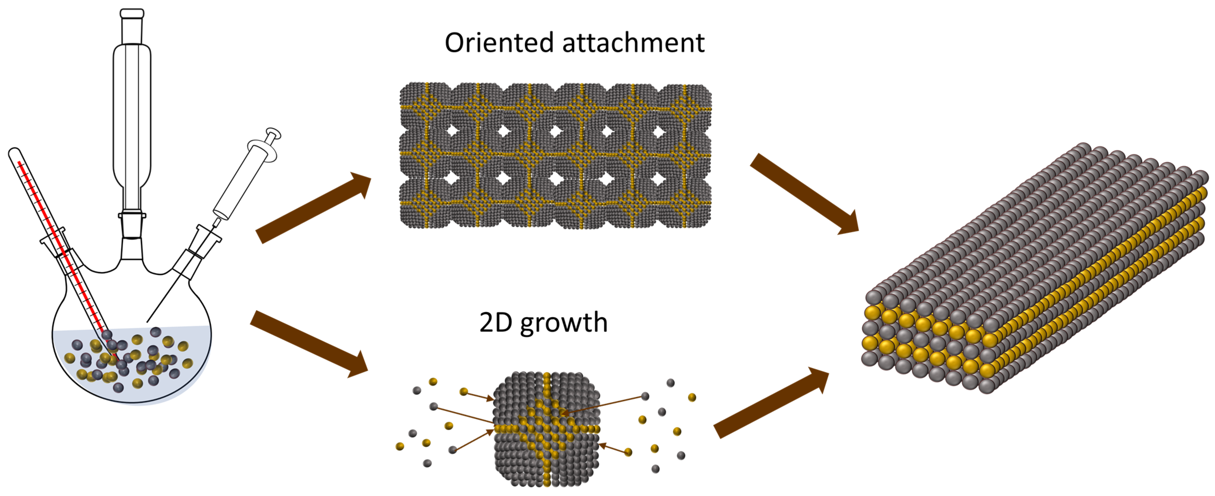
2. Synthesis Strategies
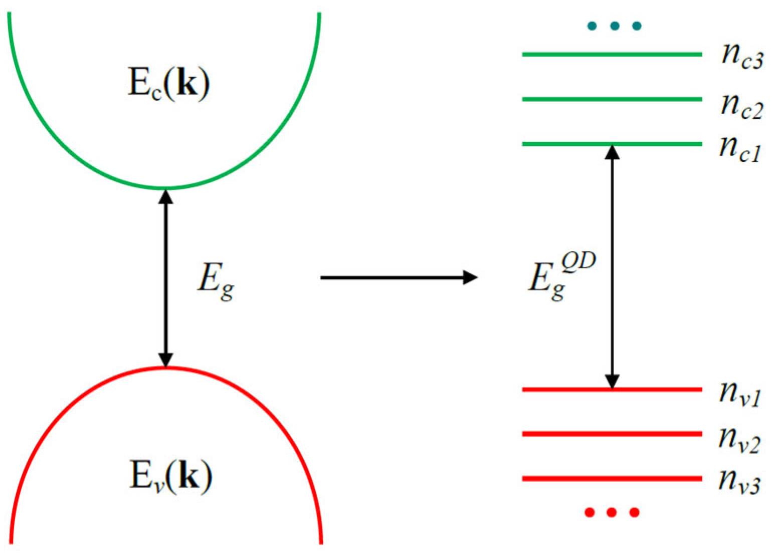
3. Optical Properties

| Original Name | Ref. | PL Peak Position (eV) | FWHM (meV) | PLQY (%) | PL Lifetime (ns) | Thickness | Lateral Sizes (nm) | Crystal Structure |
|---|---|---|---|---|---|---|---|---|
| PbSe NPls | [32] | 0.85–1.25 | 100–200 | 37 | 1200 | 0.8 ± 0.1 nm | 3–6.4 | |
| PbSe NPls | [22] | 0.8–0.93 | 80–240 | 15 | 700–2700 | 3–6 ML | ∼10–30 | rock salt |
| PbSe NPls | [40] | 1.02 | 207 | 4 ML | ∼15 × 50 | rock salt | ||
| PbS NRs | [21] | 0.69–1.13 | 130–180 | 34 | 96–372 | 1.4–2.8 nm | 20 × 50 | rock salt |
| PbS NSs | [42] | 3 | 113 | <5 nm | >1000 | zinc blend | ||
| PbS NPls | [28] | 1.66–1.69 | 106–156 | 59 to 10 | 1.8–2.3 nm | 3.5–21 | ortho-rhombic | |
| PbSe NPls | [72] | 0.95 | 108 | 600 | 5 ML | 28 × 15 | ||
| PbS NPls | [76] | 1.69 | ~122 | 1.8–2.3 nm | 47.1 ± 6.5 | ortho-rhombic | ||
| PbS NPls | [45] | 1.73 | 142 | 1.4/19.4 | 1–2 nm | 7 × 10 | rock salt | |
| PbS NSs | [46] | 0.62–0.84 | 1.2–4.6 nm | >1000 | rock salt | |||
| PbSe NPls | [25] | ∼1.13 | ∼180 | ∼0.1 | ∼2 nm | ∼30 | rock salt | |
| PbSe NPls | [33] | 1.39 | 18–64 | ∼2000 | 0.8 ± 0.1 nm | 2.7 × 4.9 | rock salt | |
| PbS/CdS Core/Shell NSs | [67] | 0.75, 0.85 after CE | ∼120 | 3.3 ± 0.1 nm, 2.1 nm after CE | >100 | |||
| PbS NSs | [27] | ∼1.08 | ∼120 | 1.2 ± 0.3 nm | ∼180 × 35 | rock-salt | ||
| PbS NSs | [70] | 0.6 to 1 | ∼70 | 4.7 to 1.2 nm | ∼20 × 20 | |||
| PbSe1−xSx NPls | [34] | from 0.9 to 1.05 | >200 | 60 | 1500 | ∼2 nm | 4–6 | rock salt |
| PbS NSs | [49] | 0.62–0.73 | 8–12 ML | 100 × 100 | ||||
| PbS and PbS/CdS NSs | [31] | 0.75 to 0.86 | 6/11 | 40/190 | 2.0 ± 0.3 to 3.6 ± 0.2 nm | 200 × 20/200 × 50/200 × 100 | ||
| QDs | Ref. | PL Peak position (eV) | FWHM (meV) | PLQY (%) | Decay Time (ns) | Size (nm) | Crystal Structure | |
| PbSe QD single | [77] | 1.55 | 100 | 30 | n/a | ~3 | Rock salt | |
| PbS QD ensemble | [78] | 0.65–1.3 | 5-50 | n/a | n/a | Rock salt | ||
| PbS QD ensemble | [79] | 0.91 | 105 | n/a | 2.6 | Rock salt | ||
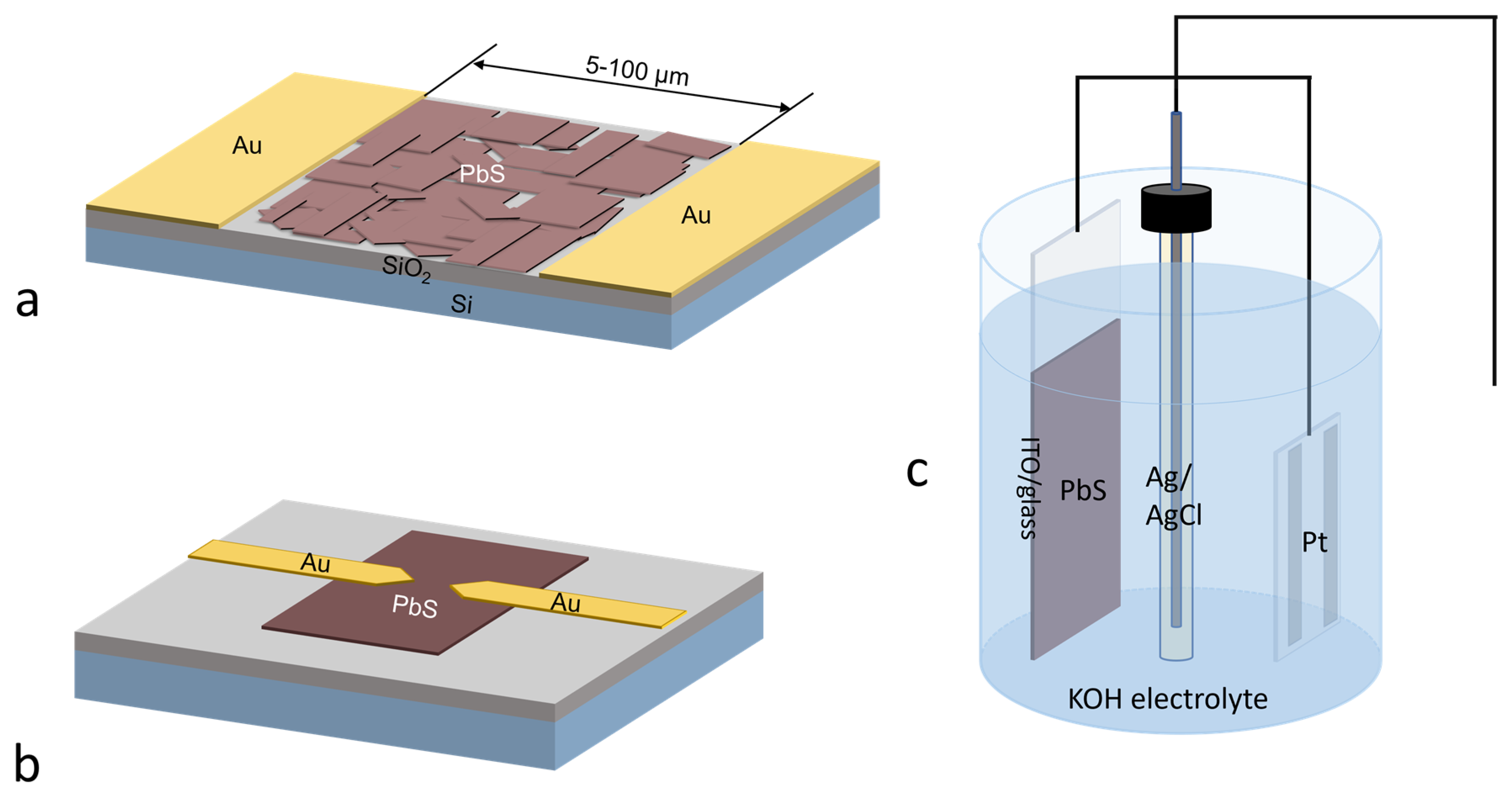
4. Applications
5. Conclusions and Outlook
Author Contributions
Funding
Data Availability Statement
Acknowledgments
Conflicts of Interest
References
- Lu, H.; Carroll, G.M.; Neale, N.R.; Beard, M.C. Infrared Quantum Dots: Progress, Challenges, and Opportunities. ACS Nano 2019, 13, 939–953. [Google Scholar] [CrossRef]
- Murphy, J.E.; Beard, M.C.; Norman, A.G.; Ahrenkiel, S.P.; Johnson, J.C.; Yu, P.; Mićić, O.I.; Ellingson, R.J.; Nozik, A.J. PbTe Colloidal Nanocrystals: Synthesis, Characterization, and Multiple Exciton Generation. J. Am. Chem. Soc 2006, 128, 3241–3247. [Google Scholar] [CrossRef]
- Mora-Seró, I. Current Challenges in the Development of Quantum Dot Sensitized Solar Cells. Adv. Energy Mater. 2020, 10, 2001774. [Google Scholar] [CrossRef]
- Zhang, M.; Liu, W.; Gong, Y.; Liu, Q.; Chen, Z. Graphene/Quantum Dot Heterostructure Photodetectors: From Material to Performance. Adv. Opt. Mater. 2022, 10, 2201889. [Google Scholar] [CrossRef]
- Yin, X.; Zhang, C.; Guo, Y.; Yang, Y.; Xing, Y.; Que, W. PbS QD-Based Photodetectors: Future-Oriented near-Infrared Detection Technology. J. Mater. Chem. C Mater. 2021, 9, 417–438. [Google Scholar] [CrossRef]
- Kim, H.S.; Yoon, K.B. Preparation and Characterization of CdS and PbS Quantum Dots in Zeolite Y and Their Applications for Nonlinear Optical Materials and Solar Cell. Coord. Chem. Rev. 2014, 263–264, 239–256. [Google Scholar] [CrossRef]
- Kim, T.; Lim, S.; Yun, S.; Jeong, S.; Park, T.; Choi, J. Design Strategy of Quantum Dot Thin-Film Solar Cells. Small 2020, 16, 2002460. [Google Scholar] [CrossRef]
- Giansante, C.; Carbone, L.; Giannini, C.; Altamura, D.; Ameer, Z.; Maruccio, G.; Loiudice, A.; Belviso, M.R.; Cozzoli, P.D.; Rizzo, A.; et al. Colloidal Arenethiolate-Capped PbS Quantum Dots: Optoelectronic Properties, Self-Assembly, and Application in Solution-Cast Photovoltaics. J. Phys. Chem. C 2013, 117, 13305–13317. [Google Scholar] [CrossRef] [Green Version]
- Semonin, O.E.; Luther, J.M.; Beard, M.C. Quantum Dots for Next-Generation Photovoltaics. Mater. Today 2012, 15, 508–515. [Google Scholar] [CrossRef]
- Al-Ahmed, A.; Afzaal, M.; Mahar, N.; Khan, F.; Pandey, S.; Zahir, M.H.; Al-Suliman, F.A. The Synergy of Lead Chalcogenide Nanocrystals in Polymeric Bulk Heterojunction Solar Cells. ACS Omega 2022, 7, 45981–45990. [Google Scholar] [CrossRef]
- Shrestha, A.; Batmunkh, M.; Tricoli, A.; Qiao, S.Z.; Dai, S. Near-Infrared Active Lead Chalcogenide Quantum Dots: Preparation, Post-Synthesis Ligand Exchange, and Applications in Solar Cells. Angew. Chem. Int. Ed. 2019, 58, 5202–5224. [Google Scholar] [CrossRef]
- Suganya, G.; Arivanandhan, M.; Kalpana, G. Investigation of Electronic Structure, Electrical and Thermal Properties of PbS Quantum Dots for Thermoelectric Applications. Mater. Sci. Semicond. Process. 2022, 148, 106789. [Google Scholar] [CrossRef]
- Litvin, A.P.; Martynenko, I.V.; Purcell-Milton, F.; Baranov, A.V.; Fedorov, A.V.; Gun’ko, Y.K. Colloidal Quantum Dots for Optoelectronics. J. Mater. Chem. A Mater. 2017, 5, 13252–13275. [Google Scholar] [CrossRef]
- Ithurria, S.; Tessier, M.D.; Mahler, B.; Lobo, R.P.S.M.; Dubertret, B.; Efros, A.L. Colloidal Nanoplatelets with Two-Dimensional Electronic Structure. Nat. Mater. 2011, 10, 936–941. [Google Scholar] [CrossRef]
- Guo, Y.; Gao, F.; Huang, P.; Wu, R.; Gu, W.; Wei, J.; Liu, F.; Li, H. Light-Emitting Diodes Based on Two-Dimensional Nanoplatelets. Energy Mater. Adv. 2022, 2022, 9857943. [Google Scholar] [CrossRef]
- Bai, B.; Zhang, C.; Dou, Y.; Kong, L.; Wang, L.; Wang, S.; Li, J.; Zhou, Y.; Liu, L.; Liu, B.; et al. Atomically Flat Semiconductor Nanoplatelets for Light-Emitting Applications. Chem. Soc. Rev. 2023, 52, 318–360. [Google Scholar] [CrossRef] [PubMed]
- Diroll, B.T.; Guzelturk, B.; Po, H.; Dabard, C.; Fu, N.; Makke, L.; Lhuillier, E.; Ithurria, S. 2D II–VI Semiconductor Nanoplatelets: From Material Synthesis to Optoelectronic Integration. Chem. Rev. 2023, 123, 3543–3624. [Google Scholar] [CrossRef]
- Shen, J.; Zhu, Y.; Jiang, H.; Li, C. 2D Nanosheets-Based Novel Architectures: Synthesis, Assembly and Applications. Nano Today 2016, 11, 483–520. [Google Scholar] [CrossRef]
- Wang, F.; Zhang, Y.; Gao, Y.; Luo, P.; Su, J.; Han, W.; Liu, K.; Li, H.; Zhai, T. 2D Metal Chalcogenides for IR Photodetection. Small 2019, 15, 1901347. [Google Scholar] [CrossRef]
- Schliehe, C.; Juarez, B.H.; Pelletier, M.; Jander, S.; Greshnykh, D.; Nagel, M.; Meyer, A.; Foerster, S.; Kornowski, A.; Klinke, C.; et al. Ultrathin PbS Sheets by Two-Dimensional Oriented Attachment. Science 2010, 329, 550–553. [Google Scholar] [CrossRef] [Green Version]
- Antu, A.D.; Jiang, Z.; Premathilka, S.M.; Tang, Y.; Hu, J.; Roy, A.; Sun, L. Bright Colloidal PbS Nanoribbons. Chem. Mater. 2018, 30, 3697–3703. [Google Scholar] [CrossRef]
- Galle, T.; Samadi Khoshkhoo, M.; Martin-Garcia, B.; Meerbach, C.; Sayevich, V.; Koitzsch, A.; Lesnyak, V.; Eychmüller, A. Colloidal PbSe Nanoplatelets of Varied Thickness with Tunable Optical Properties. Chem. Mater. 2019, 31, 3803–3811. [Google Scholar] [CrossRef]
- Kosevich, V.M.; Palatnik, L.S.; Zozulya, L.P.; Zozulya, L.F.; Sovokin, V.K. Structure Of Lead Chalcogenide Epitaxial Films On Mica. Sov. Phys. Solid State 1970, 12, 1071. [Google Scholar]
- Sato, H. Effect of Substrate Structure on Lead Chalcogenide Films. Thin Solid Film 1972, 11, 343–352. [Google Scholar] [CrossRef]
- Koh, W.; Fidler, A.F.; Dandu, N.K.; Kilina, S.V.; Klimov, V.I.; Pietryga, J.M.; Fidler, A.F.; Klimov, V.I.; Pietryga, J.M.; Kilina, S.V.; et al. Thickness-Controlled Quasi-Two-Dimensional Colloidal PbSe Nanoplatelets. J. Am. Chem. Soc. 2017, 139, 2152–2155. [Google Scholar] [CrossRef] [PubMed]
- Lee, S.; Lee, D.T.; Ko, J.H.; Kim, W.J.; Joo, J.; Jeong, S.; McGuire, J.A.; Kim, Y.H.; Lee, D.C. Slow Colloidal Growth of PbSe Nanocrystals for Facile Morphology and Size Control. RSC Adv. 2014, 4, 9842–9850. [Google Scholar] [CrossRef]
- Akkerman, Q.A.; Martín-García, B.; Buha, J.; Almeida, G.; Toso, S.; Marras, S.; Bonaccorso, F.; Petralanda, U.; Infante, I.; Manna, L. Ultrathin Orthorhombic PbS Nanosheets. Chem. Mater. 2019, 31, 8145–8153. [Google Scholar] [CrossRef]
- Khan, A.H.; Brescia, R.; Polovitsyn, A.; Angeloni, I.; Martín-García, B.; Moreels, I. Near-Infrared Emitting Colloidal PbS Nanoplatelets: Lateral Size Control and Optical Spectroscopy. Chem. Mater. 2017, 29, 2883–2889. [Google Scholar] [CrossRef] [Green Version]
- Macias-Pinilla, D.F.; Echeverría-Arrondo, C.; Gualdrón Reyes, A.F.; Agouram, S.; Muñoz-Sanjosé, V.; Planelles, J.; Mora-Seró, I.; Climente, J.I. Morphology and Band Structure of Orthorhombic PbS Nanoplatelets: An Indirect Band Gap Material. Chem. Mater. 2021, 33, 420–429. [Google Scholar] [CrossRef]
- Khan, A.H.; Pal, S.; Dalui, A.; Pradhan, J.; Sarma, D.D.; Acharya, S. Solution-Processed Free-Standing Ultrathin Two-Dimensional PbS Nanocrystals with Efficient and Highly Stable Dielectric Properties. Chem. Mater. 2017, 29, 1175–1182. [Google Scholar] [CrossRef]
- Zhang, H.; Savitzky, B.H.; Yang, J.; Newman, J.T.; Perez, K.A.; Hyun, B.-R.R.; Kourkoutis, L.F.; Hanrath, T.; Wise, F.W. Colloidal Synthesis of PbS and PbS/CdS Nanosheets Using Acetate-Free Precursors. Chem. Mater. 2016, 28, 127–134. [Google Scholar] [CrossRef]
- Klepzig, L.F.; Biesterfeld, L.; Romain, M.; Niebur, A.; Schlosser, A.; Hübner, J.; Lauth, J. Colloidal 2D PbSe Nanoplatelets with Efficient Emission Reaching the Telecom O-, E- and S-Band. Nanoscale Adv. 2022, 4, 590–599. [Google Scholar] [CrossRef] [PubMed]
- Biesterfeld, L.; Klepzig, L.F.; Niebur, A.; Rosebrock, M.; Lauth, J. Toward Bright Colloidal Near-Infrared Emitters: Surface Passivation of 2D PbSe Nanoplatelets by Metal Halides. J. Phys. Chem. C 2022, 126, 19277–19285. [Google Scholar] [CrossRef]
- Zhou, Y.; Celikin, M.; Camellini, A.; Sirigu, G.; Tong, X.; Jin, L.; Basu, K.; Tong, X.; Barba, D.; Ma, D.; et al. Ultrasmall Nanoplatelets: The Ultimate Tuning of Optoelectronic Properties. Adv. Energy Mater. 2017, 7, 1602728. [Google Scholar] [CrossRef]
- Salzmann, B.B.V.; de Wit, J.; Li, C.; Arenas-Esteban, D.; Bals, S.; Meijerink, A.; Vanmaekelbergh, D. Two-Dimensional CdSe-PbSe Heterostructures and PbSe Nanoplatelets: Formation, Atomic Structure, and Optical Properties. J. Phys. Chem. C 2022, 126, 1513–1522. [Google Scholar] [CrossRef]
- Wu, W.-Y.; Chakrabortty, S.; Guchhait, A.; Wong, G.Y.Z.; Dalapati, G.K.; Lin, M.; Chan, Y. Solution-Processed 2D PbS Nanoplates with Residual Cu 2 S Exhibiting Low Resistivity and High Infrared Responsivity. Chem. Mater. 2016, 28, 9132–9138. [Google Scholar] [CrossRef]
- Gao, L.; Chen, H.; Wang, R.; Wei, S.; Kuklin, A.V.; Mei, S.; Zhang, F.; Zhang, Y.; Jiang, X.; Luo, Z.; et al. Ultra-Small 2D PbS Nanoplatelets: Liquid-Phase Exfoliation and Emerging Applications for Photo-Electrochemical Photodetectors. Small 2021, 17, 2005913. [Google Scholar] [CrossRef]
- Sonntag, L.; Shamraienko, V.; Fan, X.; Khoshkhoo, M.S.; Kneppe, D.; Koitzsch, A.; Gemming, T.; Hiekel, K.; Leo, K.; Lesnyak, V.; et al. Colloidal PbS Nanoplatelets Synthesized: Via Cation Exchange for Electronic Applications. Nanoscale 2019, 11, 19370–19379. [Google Scholar] [CrossRef] [Green Version]
- Guo, J.; Cao, Y.; Shi, R.; Waterhouse, G.I.N.; Wu, L.; Tung, C.; Zhang, T. A Photochemical Route towards Metal Sulfide Nanosheets from Layered Metal Thiolate Complexes. Angew. Chem. 2019, 58, 8443–8447. [Google Scholar] [CrossRef]
- Galle, T.; Spittel, D.; Weiß, N.; Shamraienko, V.; Decker, H.; Georgi, M.; Hübner, R.; Metzkow, N.; Steinbach, C.; Schwarz, D.; et al. Simultaneous Ligand and Cation Exchange of Colloidal CdSe Nanoplatelets toward PbSe Nanoplatelets for Application in Photodetectors. J. Phys. Chem. Lett. 2021, 12, 5214–5220. [Google Scholar] [CrossRef]
- Liu, Y.; Lim, C.-K.; Fu, Z.; Yin, D.; Swihart, M.T. Can the Morphology of Biconcave Metal Sulfide Nanoplatelets Be Preserved during Cation Exchange? Chem. Mater. 2019, 31, 5706–5712. [Google Scholar] [CrossRef]
- Shkir, M.; AlFaify, S.; Ganesh, V.; Yahia, I.S. Facile One Pot Synthesis of PbS Nanosheets and Their Characterization. Solid State Sci. 2017, 70, 81–85. [Google Scholar] [CrossRef]
- Li, X.; Hu, J.; Wang, Y.; Feng, J. PbSe Nanosheets for High-Performance Harmonic Mode Locking. Ann. Phys. 2022, 534, 2200183. [Google Scholar] [CrossRef]
- Bielewicz, T.; Dogan, S.; Klinke, C. Tailoring the Height of Ultrathin PbS Nanosheets and Their Application as Field-Effect Transistors. Small 2015, 11, 826–833. [Google Scholar] [CrossRef] [PubMed] [Green Version]
- Manteiga Vázquez, F.; Yu, Q.; Klepzig, L.F.; Siebbeles, L.D.A.; Crisp, R.W.; Lauth, J. Probing Excitons in Ultrathin PbS Nanoplatelets with Enhanced Near-Infrared Emission. J. Phys. Chem. Lett. 2021, 12, 680–685. [Google Scholar] [CrossRef]
- Bhandari, G.B.; Subedi, K.; He, Y.; Jiang, Z.; Leopold, M.; Reilly, N.; Lu, H.P.; Zayak, A.T.; Sun, L. Thickness-Controlled Synthesis of Colloidal PbS Nanosheets and Their Thickness-Dependent Energy Gaps. Chem. Mater. 2014, 26, 5433–5436. [Google Scholar] [CrossRef]
- Acharya, S.; Das, B.; Thupakula, U.; Ariga, K.; Sarma, D.D.; Israelachvili, J.; Golan, Y. A Bottom-Up Approach toward Fabrication of Ultrathin PbS Sheets. Nano Lett. 2013, 13, 409–415. [Google Scholar] [CrossRef]
- Yan, C.; Chen, G.; Shi, X.; Pei, J.; Sun, J.; Chen, D.; Zhang, Y. The S-Hindered Synthesis of PbSe/PbS Nanosheets with Enhanced Electrochemical Activities. New J. Chem. 2015, 39, 3513–3519. [Google Scholar] [CrossRef]
- Premathilaka, S.M.; Jiang, Z.; Antu, A.; Leffler, J.; Hu, J.; Roy, A.; Sun, L. A Robust Method for the Synthesis of Colloidal PbS Nanosheets. Phys. Status Solidi (RRL) Rapid Res. Lett. 2016, 10, 838–842. [Google Scholar] [CrossRef]
- Madelung, O.; Rössler, U.; Schulz, M. Semiconductors: Group IV Elements, IV–IV and III–IV Compounds. In Landolt-Börnstein, New Series, Group III; Springer: Berlin/Heidelberg, Germany, 2005; Volume 41. [Google Scholar]
- Moayed, M.M.R.; Bielewicz, T.; Zöllner, M.S.; Herrmann, C.; Klinke, C. Towards Colloidal Spintronics through Rashba Spin-Orbit Interaction in Lead Sulphide Nanosheets. Nat. Commun. 2017, 8, 2–8. [Google Scholar] [CrossRef] [Green Version]
- Wise, F.W. Lead Salt Quantum Dots: The Limit of Strong Quantum Confinement. Acc. Chem. Res. 2000, 33, 773–780. [Google Scholar] [CrossRef]
- Allan, G.; Delerue, C. Confinement Effects in PbSe Quantum Wells and Nanocrystals. Phys. Rev. B 2004, 70, 245321. [Google Scholar] [CrossRef]
- Wan, W.; Yao, Y.; Sun, L.; Liu, C.; Zhang, F. Topological, Valleytronic, and Optical Properties of Monolayer PbS. Adv. Mater. 2017, 29, 1604788. [Google Scholar] [CrossRef] [PubMed] [Green Version]
- Yang, J.; Wise, F.W. Electronic States of Lead-Salt Nanosheets. J. Phys. Chem. C 2015, 119, 26809–26816. [Google Scholar] [CrossRef]
- Baghdasaryan, D.A.; Harutyunyan, V.A.; Hayrapetyan, D.B.; Kazaryan, E.M.; Baskoutas, S.; Sarkisyan, H.A. Exciton States and Optical Absorption in CdSe and PbS Nanoplatelets. Nanomaterials 2022, 12, 3690. [Google Scholar] [CrossRef] [PubMed]
- Goupalov, S.V. Carrier Confinement and Interband Optical Transitions in Lead Chalcogenide Quantum Wells, Nanosheets, and Nanoplatelets. Nanoscale 2023, 15, 1230–1235. [Google Scholar] [CrossRef]
- Zhang, J.; Pang, J.; Chen, H.; Wei, G.; Wei, S.; Yan, J.; Jin, S. Study on SO 2 and Cl 2 Sensor Application of 2D PbSe Based on First Principles Calculations. RSC Adv. 2022, 12, 8530–8535. [Google Scholar] [CrossRef] [PubMed]
- Rytova, N.S. Screened Potential of a Point Charge in a Thin Film. arXiv 2018, arXiv:1806.00976. [Google Scholar]
- Keldysh, L.V. Coulomb Interaction in Thin Semiconductor and Semimetalic Films. Sov. J. Exp. Theor. Phys. Lett. 1979, 29, 716–719. [Google Scholar]
- Keldysh, L.V. Excitons in Semiconductor–Dielectric Nanostructures. Phys. Status Solidi (a) 1997, 164, 3–12. [Google Scholar] [CrossRef]
- Available online: https://www.quantum-espresso.org (accessed on 30 April 2023).
- Perdew, J.P.; Burke, K.; Ernzerhof, M. Generalized Gradient Approximation Made Simple. Phys. Rev. Lett. 1996, 77, 3865–3868. [Google Scholar] [CrossRef] [Green Version]
- Kirchner-Hall, N.E.; Zhao, W.; Xiong, Y.; Timrov, I.; Dabo, I. Extensive Benchmarking of DFT+U Calculations for Predicting Band Gaps. Appl. Sci. 2021, 11, 2395. [Google Scholar] [CrossRef]
- Available online: https://www.vasp.at (accessed on 30 April 2023).
- Paier, J.; Marsman, M.; Hummer, K.; Kresse, G.; Gerber, I.C.; Ángyán, J.G. Screened Hybrid Density Functionals Applied to Solids. J. Chem. Phys. 2006, 124, 154709. [Google Scholar] [CrossRef] [PubMed] [Green Version]
- Hu, J.; Premathilka, S.M.; Jiang, Z.; Roland, P.J.; Voevodin, A.A.; Ellingson, R.J.; Sun, L.; Khan, S.; Antu, A. Few-Atom-Thick Colloidal PbS/CdS Core/Shell Nanosheets. Chem. Mater. 2016, 28, 5342–5346. [Google Scholar] [CrossRef]
- Liu, J.; Qian, X.; Fu, L. Crystal Field Effect Induced Topological Crystalline Insulators in Monolayer IV–VI Semiconductors. Nano Lett. 2015, 15, 2657–2661. [Google Scholar] [CrossRef] [Green Version]
- Barone, P.; Rauch, T.; Di Sante, D.; Henk, J.; Mertig, I.; Picozzi, S. Pressure-Induced Topological Phase Transitions in Rocksalt Chalcogenides. Phys. Rev. B 2013, 88, 045207. [Google Scholar] [CrossRef] [Green Version]
- Weeraddana, T.M.; Premathilaka, S.M.; Tang, Y.; Antu, A.D.; Roach, A.; Yang, J.; Sun, L. Dielectrically Confined Stable Excitons in Few-Atom-Thick PbS Nanosheets. J. Phys. Chem. Lett. 2022, 13, 7756–7761. [Google Scholar] [CrossRef] [PubMed]
- Zhang, J.; Jiang, X. Confinement-Dependent Below-Gap State in PbS Quantum Dot Films Probed by Continuous-Wave Photoinduced Absorption. J. Phys. Chem. B 2008, 112, 9557–9560. [Google Scholar] [CrossRef]
- Skurlov, I.; Sokolova, A.; Galle, T.; Cherevkov, S.; Ushakova, E.; Baranov, A.; Lesnyak, V.; Fedorov, A.; Litvin, A. Temperature-Dependent Photoluminescent Properties of PbSe Nanoplatelets. Nanomaterials 2020, 10, 2570. [Google Scholar] [CrossRef]
- Lakowicz, J.R. Introduction to Fluorecence. In Principles of Fluorescence Spectroscopy; Springer Science + Business Media, LLC: Berlin/Heidelberg, Germany, 2006; pp. 1–26. [Google Scholar]
- Zhang, Y.; Zherebetskyy, D.; Bronstein, N.D.; Barja, S.; Lichtenstein, L.; Alivisatos, A.P.; Wang, L.-W.; Salmeron, M. Molecular Oxygen Induced In-Gap States in PbS Quantum Dots. ACS Nano 2015, 9, 10445–10452. [Google Scholar] [CrossRef] [Green Version]
- Zherebetskyy, D.; Zhang, Y.; Salmeron, M.; Wang, L.-W. Tolerance of Intrinsic Defects in PbS Quantum Dots. J. Phys. Chem. Lett. 2015, 6, 4711–4716. [Google Scholar] [CrossRef]
- Sánchez-Godoy, H.E.; Erazo, E.A.; Gualdrón-Reyes, A.F.; Khan, A.H.; Agouram, S.; Barea, E.M.; Rodriguez, R.A.; Zarazúa, I.; Ortiz, P.; Cortés, M.T.; et al. Preferred Growth Direction by PbS Nanoplatelets Preserves Perovskite Infrared Light Harvesting for Stable, Reproducible, and Efficient Solar Cells. Adv. Energy Mater. 2020, 10, 2002422. [Google Scholar] [CrossRef]
- Peterson, J.J.; Krauss, T.D. Fluorescence Spectroscopy of Single Lead Sulfide Quantum Dots. Nano Lett. 2006, 6, 510–514. [Google Scholar] [CrossRef] [PubMed]
- Semonin, O.E.; Johnson, J.C.; Luther, J.M.; Midgett, A.G.; Nozik, A.J.; Beard, M.C. Absolute Photoluminescence Quantum Yields of IR-26 Dye, PbS, and PbSe Quantum Dots. J. Phys. Chem. Lett. 2010, 1, 2445–2450. [Google Scholar] [CrossRef]
- Liu, C.; Kwon, Y.K.; Heo, J. Laser-Induced Blue-Shift of the Photoluminescence from PbS Quantum Dots in Glasses. Chem. Phys. Lett. 2008, 452, 281–284. [Google Scholar] [CrossRef]
- Ithurria, S.; Bousquet, G.; Dubertret, B. Continuous Transition from 3D to 1D Confinement Observed during the Formation of CdSe Nanoplatelets. J. Am. Chem. Soc. 2011, 133, 3070–3077. [Google Scholar] [CrossRef] [PubMed]
- Aerts, M.; Bielewicz, T.; Klinke, C.; Grozema, F.C.; Houtepen, A.J.; Schins, J.M.; Siebbeles, L.D.A. Highly Efficient Carrier Multiplication in PbS Nanosheets. Nat. Commun. 2014, 5, 3789. [Google Scholar] [CrossRef] [Green Version]
- Beard, M.C.; Luther, J.M.; Semonin, O.E.; Nozik, A.J. Third Generation Photovoltaics Based on Multiple Exciton Generation in Quantum Confined Semiconductors. Acc. Chem. Res. 2013, 46, 1252–1260. [Google Scholar] [CrossRef]
- Dogan, S.; Bielewicz, T.; Cai, Y.; Klinke, C. Field–Effect Transistors Made of Individual Colloidal PbS Nanosheets. Appl. Phys. Lett. 2012, 101, 073102. [Google Scholar] [CrossRef] [Green Version]
- Pedrueza, E.; Segura, A.; Abargues, R.; Bailach, J.B.; Chervin, J.C.; Martínez-Pastor, J.P. The Effect of Quantum Size Confinement on the Optical Properties of PbSe Nanocrystals as a Function of Temperature and Hydrostatic Pressure. Nanotechnology 2013, 24, 205701. [Google Scholar] [CrossRef]
- Lauth, J.; Failla, M.; Klein, E.; Klinke, C.; Kinge, S.; Siebbeles, L.D.A. Photoexcitation of PbS Nanosheets Leads to Highly Mobile Charge Carriers and Stable Excitons. Nanoscale 2019, 11, 21569–21576. [Google Scholar] [CrossRef] [PubMed] [Green Version]
- Konstantatos, G.; Howard, I.; Fischer, A.; Hoogland, S.; Clifford, J.; Klem, E.; Levina, L.; Sargent, E.H. Ultrasensitive Solution-Cast Quantum Dot Photodetectors. Nature 2006, 442, 180–183. [Google Scholar] [CrossRef]
- Wu, Y.; Wang, Y.; Wang, M.; Sun, N.; Li, C. GRIN2A Polymorphisms and Expression Levels Are Associated with Lead-Induced Neurotoxicity. Toxicol. Ind. Health 2017, 33, 332–339. [Google Scholar] [CrossRef]
- Jia, Q.; HA, X.; Yang, Z.; Hui, L.; Yang, X. Oxidative Stress: A Possible Mechanism for Lead-Induced Apoptosis and Nephrotoxicity. Toxicol. Mech. Methods 2012, 22, 705–710. [Google Scholar] [CrossRef] [PubMed]
- EU. Directive 2011/65/EU of the European Parliament and of the Council of 8 June 2011 on the Restriction of the Use of Certain Hazardous Substances in Electrical and Electronic Equipment; EU: Brussels, Belgium, 2011. [Google Scholar]
- Turyanska, L.; Bradshaw, T.D.; Sharpe, J.; Li, M.; Mann, S.; Thomas, N.R.; Patanè, A. The Biocompatibility of Apoferritin-Encapsulated PbS Quantum Dots. Small 2009, 5, 1738–1741. [Google Scholar] [CrossRef] [PubMed]
- Hu, R.; Law, W.-C.; Lin, G.; Ye, L.; Liu, J.; Liu, J.; Reynolds, J.L.; Yong, K.-T. PEGylated Phospholipid Micelle-Encapsulated Near-Infrared PbS Quantum Dots for in Vitro and in Vivo Bioimaging. Theranostics 2012, 2, 723–733. [Google Scholar] [CrossRef] [Green Version]
- Moody, N.; Yoon, D.; Johnson, A.; Wassweiler, E.; Nasilowski, M.; Bulović, V.; Bawendi, M.G. Decreased Synthesis Costs and Waste Product Toxicity for Lead Sulfide Quantum Dot Ink Photovoltaics. Adv. Sustain. Syst. 2019, 3, 1900061. [Google Scholar] [CrossRef]
- Yong, K.-T.; Law, W.-C.; Hu, R.; Ye, L.; Liu, L.; Swihart, M.T.; Prasad, P.N. Nanotoxicity Assessment of Quantum Dots: From Cellular to Primate Studies. Chem. Soc. Rev. 2013, 42, 1236–1250. [Google Scholar] [CrossRef]
- Konstantatos, G.; Sargent, E.H. Nanostructured Materials for Photon Detection. Nat. Nanotechnol. 2010, 5, 391–400. [Google Scholar] [CrossRef]
- Grüning, M.; Marini, A.; Rubio, A. Density Functionals from Many-Body Perturbation Theory: The Band Gap for Semiconductors and Insulators. J. Chem. Phys. 2006, 124, 154108. [Google Scholar] [CrossRef] [Green Version]
- Kotliar, G.; Savrasov, S.Y.; Haule, K.; Oudovenko, V.S.; Parcollet, O.; Marianetti, C.A. Electronic Structure Calculations with Dynamical Mean-Field Theory. Rev. Mod. Phys. 2006, 78, 865–951. [Google Scholar] [CrossRef] [Green Version]
- Chatterjee, A.; Biswas, K. Solution-Based Synthesis of Layered Intergrowth Compounds of the Homologous PbmBi2nTe3n+m Series as Nanosheets. Angew. Chem. Int. Ed. 2015, 54, 5623–5627. [Google Scholar] [CrossRef] [PubMed]
- Zhu, T.J.; Chen, X.; Meng, X.Y.; Zhao, X.B.; He, J. Anisotropic Growth of Cubic PbTe Nanoparticles to Nanosheets: Controlled Synthesis and Growth Mechanisms. Cryst. Growth Des. 2010, 10, 3727–3731. [Google Scholar] [CrossRef]
- Jin, R.; Chen, G.; Pei, J.; Sun, J.; Wang, Q. Controllable Synthesis and Thermoelectric Transport Properties of Binary-Phased PbTe/PbSe Nanocrystals. CrystEngComm 2012, 14, 4461–4466. [Google Scholar] [CrossRef]

| Original Name | Ref. | Synthesis Method | Thickness | Lateral Sizes, nm | Crystal Structure |
|---|---|---|---|---|---|
| PbS NPls | [38] | CE (PbO, OA, 100 °C) from CuS | 5 nm | 40 | rock salt |
| PbSe NPls | [32] | Direct (Pb(OA)2, HOA, 0 °C) | 0.8 ± 0.1 nm | 3–6.4 | |
| PbS NSs | [39] | Direct (photochemical) | 1.4 nm | >200 | |
| PbSe NPls | [22] | CE (PbBr2, OlAm, 80 °C) from CdSe | 3–6 ML | ∼10–30 | rock salt |
| PbSe NPls | [40] | CE + ligand exchange (PbI2 and NH4I) from CdSe | 4 ML | ∼15 × 50 | rock salt |
| PbS NRs | [21] | Direct (PbO, OA, thioacetamide, DMF 100 °C) | 1.4–2.8 nm | 20 × 50 | rock salt |
| Biconcave PbS NPls | [41] | CE from Cu1.94S | ∼2.5 nm | ∼25 | rock salt |
| PbS NSs | [42] | Direct (Pb(OAc)2, thiourea, sodium dodecyl sulfate, NaOH, 60 °C) | <5 nm | >1000 | zinc blend |
| PbS NPls | [28] | Single molecule precursor (Chugaev reaction with lead octadecyl xanthate, TOA, 80–90 °C) | 1.8–2.3 nm | 3.5–21 | orthorhombic |
| PbSe NSs | [43] | Direct (PbCl2, selenium powder, 220 °C) | >100 | ||
| PbS NSs | [44] | Direct (thioacetamide, DMF, TOP, PbOAc, OA) | 4, 6, 16, 23 nm | >100 | rock salt |
| PbS NPls | [45] | Direct (lead oleate, octylamine, thiourea, OA, room temperature) | 1–2 nm | 7 × 10 | rock salt |
| PbS NPls | [37] | Liquid-phase exfoliation | 3.7 ± 0.9 nm | 11.2 ± 1.7 | |
| PbS NPls | [36] | CE (lead oleate) from Cu2S | ~3.5 nm | ~120–150 | |
| PbS NSs | [20] | Oriented attachment | 2.2 nm | >200 | rock salt |
| PbS NSs | [46] | Oriented attachment | 1.2–4.6 nm | >1000 | rock salt |
| PbSe NPls | [25] | Oriented attachment (PbCl2 and Se powder react in a mixture of alkyl amines) | ∼2 nm | rock salt | |
| PbS NSs | [27] | Single molecule precursor (Pb(SCN)2, ODE, OA, 165 °C) | 1.2 ± 0.3 nm | ∼35–180 | orthorhombic/rock salt |
| PbSe1−xSx NPls | [34] | CE (var. PbCl2, PbBr2, PbI2, Pb(oleate)2) from CdSe1−xSx | ∼2 nm | 4–6 | rock salt |
| PbS NSs | [47] | Coalescence of PbS nanowires | 1.8 nm | 200-20000 | |
| PbSe NC | [26] | Direct (PbO, OA, Se, TOP, 130 °C) | 4.3 ± 0.5 nm | 200 | |
| PbSe/PbS NSs | [48] | Direct (one pot autoclave) | 10–30 nm | 250–350 | |
| PbS NSs | [49] | Oriented attachment (PbO modification) | 8–12 ML | 100 × 100 | |
| PbS and PbS/CdS NSs | [31] | Direct ((PbO) and bis(trimethylsilyl)sulfide, 90 °C) | 2.0 ± 0.3/3.6 ± 0.2 nm | 200 × 20, 200 × 50, 200 × 100 | |
| 2D PbS NC | [30] | Single molecule (lead hexadecyl xanthate and TOA at 60 °C) | ∼2 nm | 180 × 40 | rocksalt |
Disclaimer/Publisher’s Note: The statements, opinions and data contained in all publications are solely those of the individual author(s) and contributor(s) and not of MDPI and/or the editor(s). MDPI and/or the editor(s) disclaim responsibility for any injury to people or property resulting from any ideas, methods, instructions or products referred to in the content. |
© 2023 by the authors. Licensee MDPI, Basel, Switzerland. This article is an open access article distributed under the terms and conditions of the Creative Commons Attribution (CC BY) license (https://creativecommons.org/licenses/by/4.0/).
Share and Cite
Babaev, A.A.; Skurlov, I.D.; Timkina, Y.A.; Fedorov, A.V. Colloidal 2D Lead Chalcogenide Nanocrystals: Synthetic Strategies, Optical Properties, and Applications. Nanomaterials 2023, 13, 1797. https://doi.org/10.3390/nano13111797
Babaev AA, Skurlov ID, Timkina YA, Fedorov AV. Colloidal 2D Lead Chalcogenide Nanocrystals: Synthetic Strategies, Optical Properties, and Applications. Nanomaterials. 2023; 13(11):1797. https://doi.org/10.3390/nano13111797
Chicago/Turabian StyleBabaev, Anton A., Ivan D. Skurlov, Yulia A. Timkina, and Anatoly V. Fedorov. 2023. "Colloidal 2D Lead Chalcogenide Nanocrystals: Synthetic Strategies, Optical Properties, and Applications" Nanomaterials 13, no. 11: 1797. https://doi.org/10.3390/nano13111797
APA StyleBabaev, A. A., Skurlov, I. D., Timkina, Y. A., & Fedorov, A. V. (2023). Colloidal 2D Lead Chalcogenide Nanocrystals: Synthetic Strategies, Optical Properties, and Applications. Nanomaterials, 13(11), 1797. https://doi.org/10.3390/nano13111797