
Research Progress on Metal–Organic Frameworks by Advanced Transmission Electron Microscopy


Abstract
1. Introduction
2. Challenges and Chances of TEM Studies
2.1. Damage Mechanisms
2.2. Strategies for Minimizing Damages
2.2.1. Low-Dose TEM
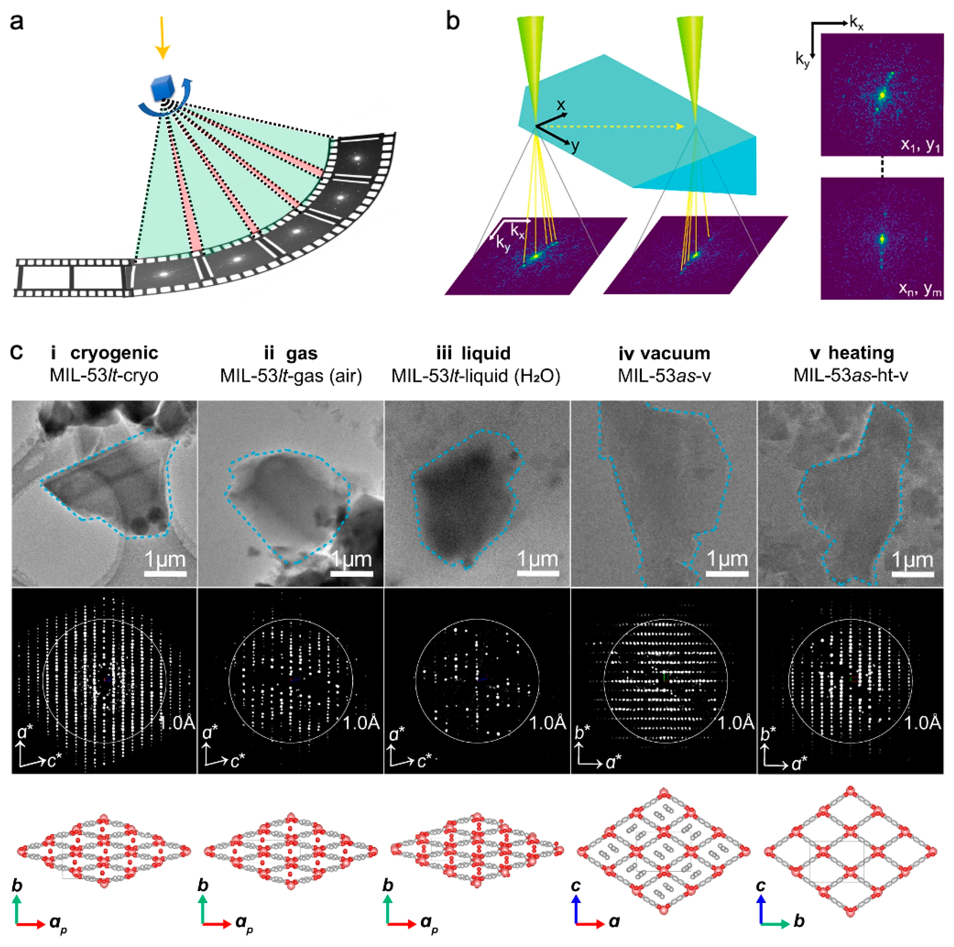
2.2.2. Cryo-TEM

3. Strategies, Techniques, and Research Advances
3.1. Traditional and Advanced Electron Diffraction

3.2. TEM and DDEC Camera
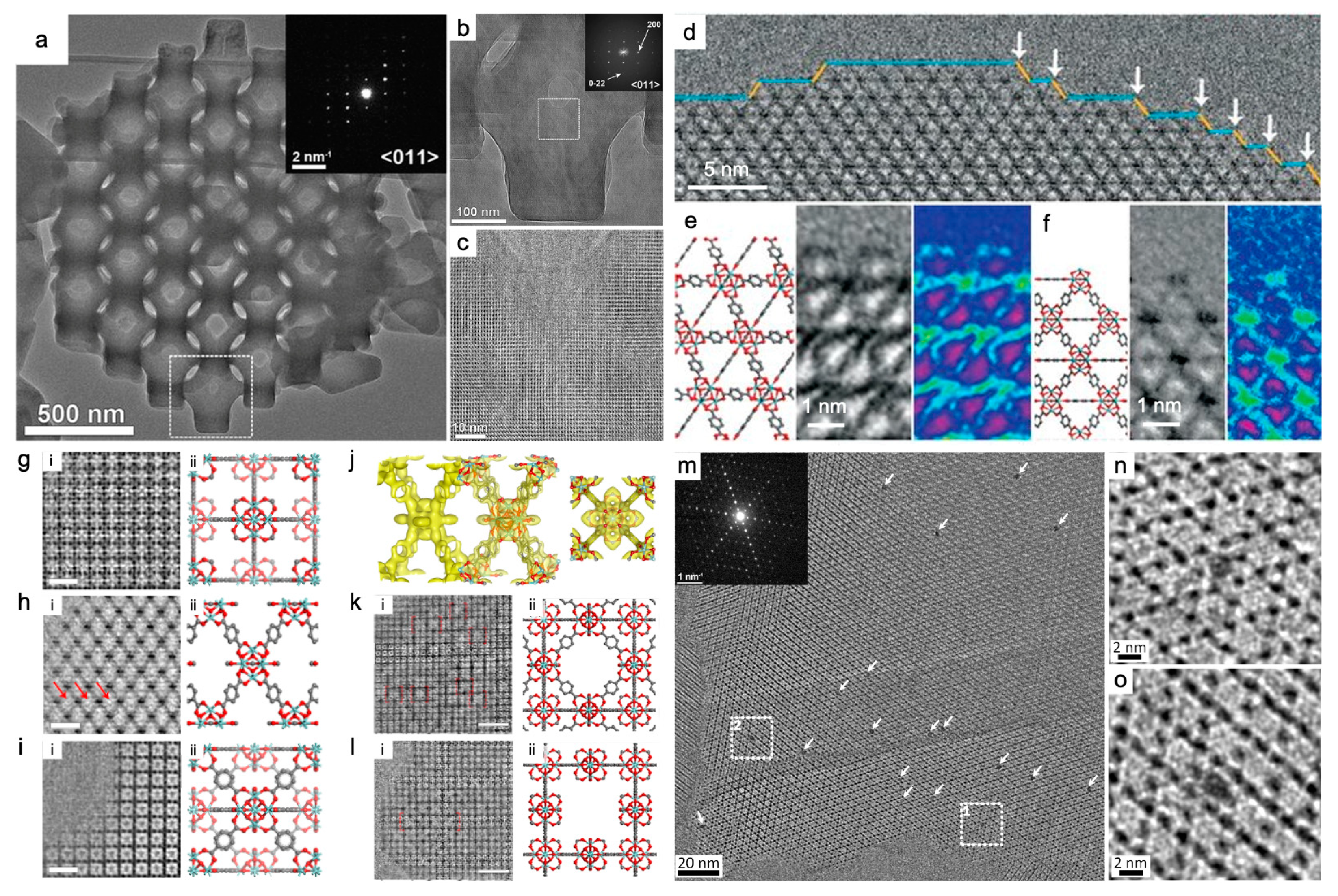
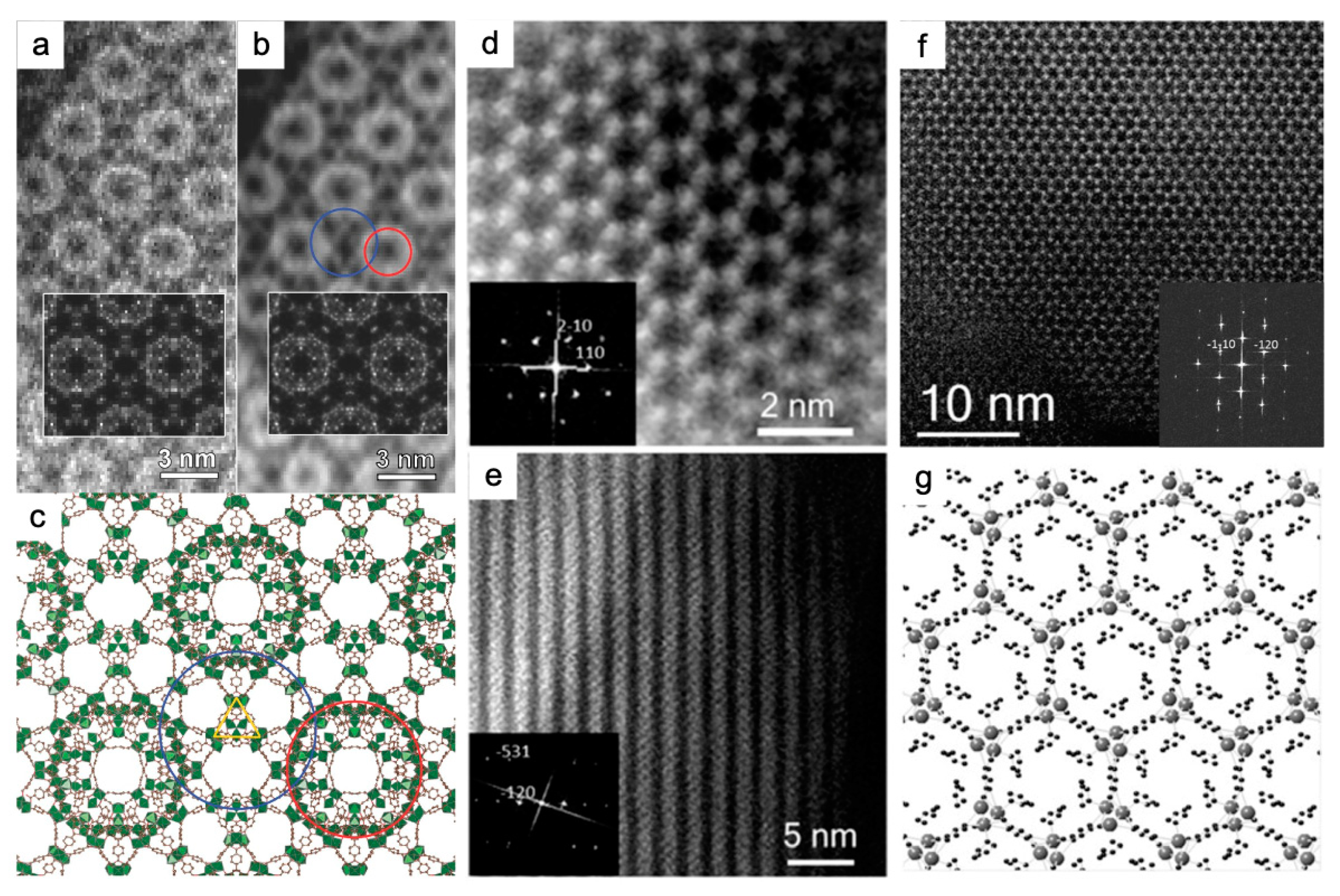
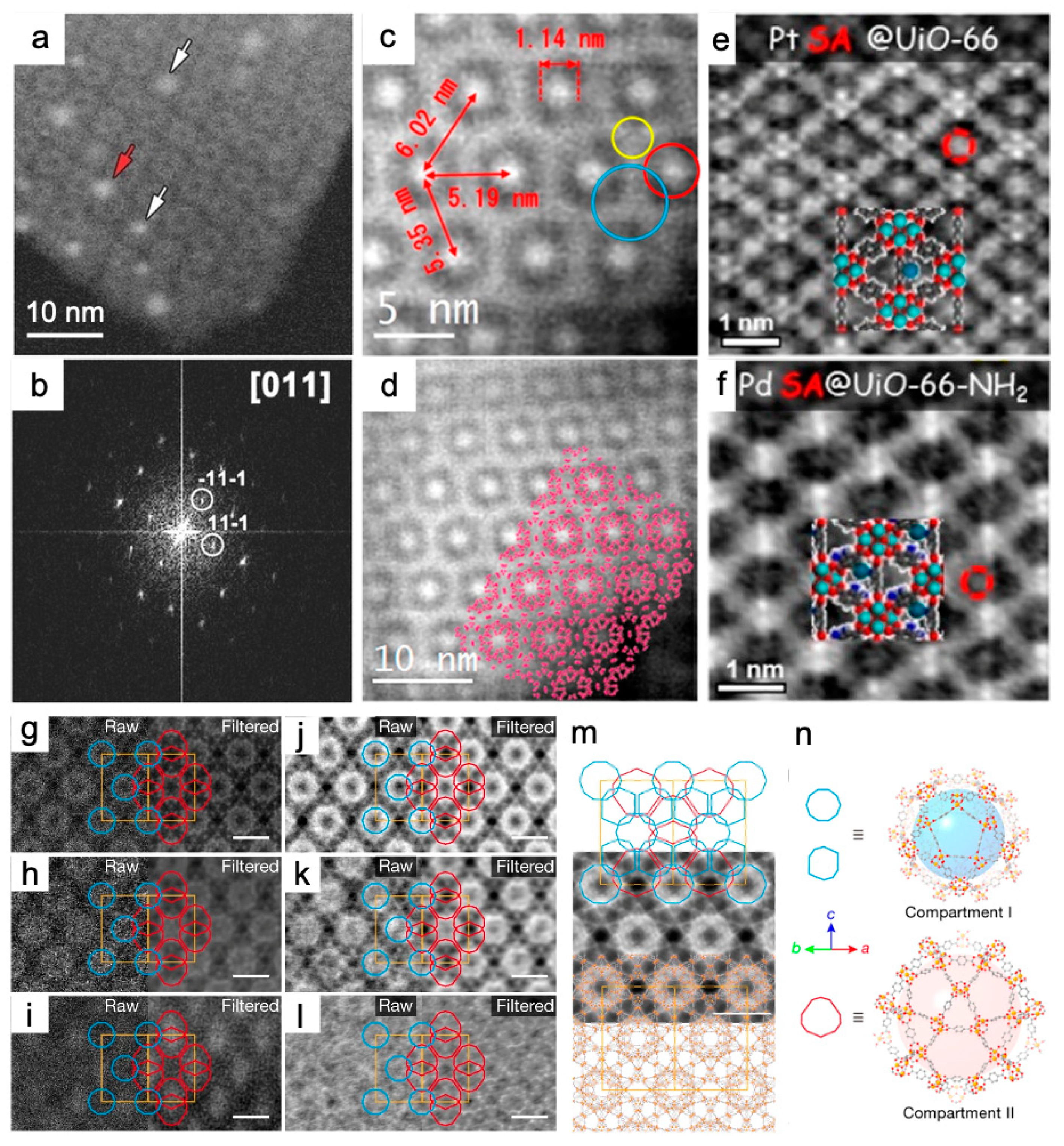
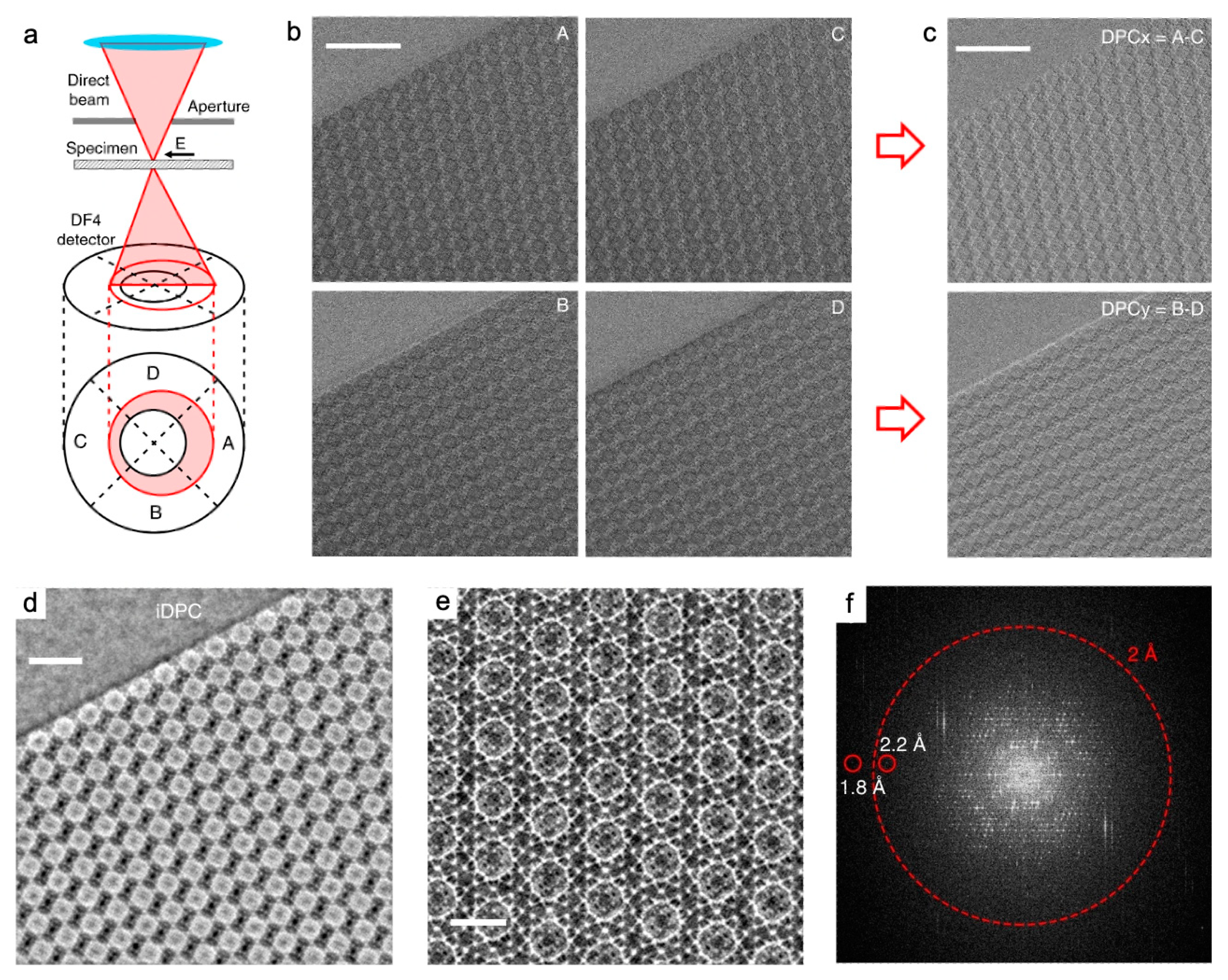
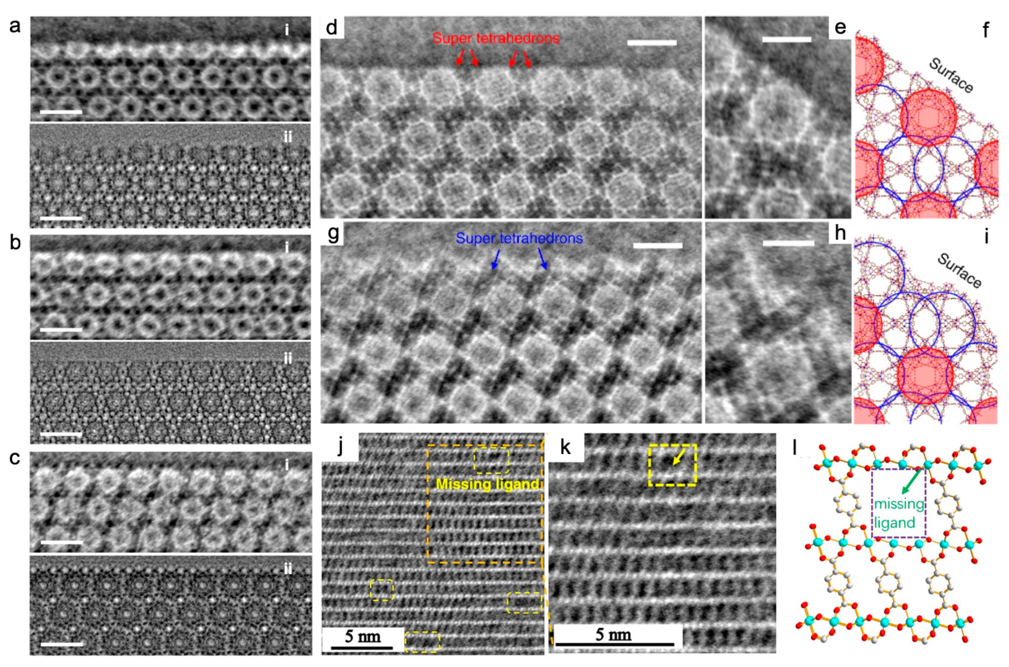
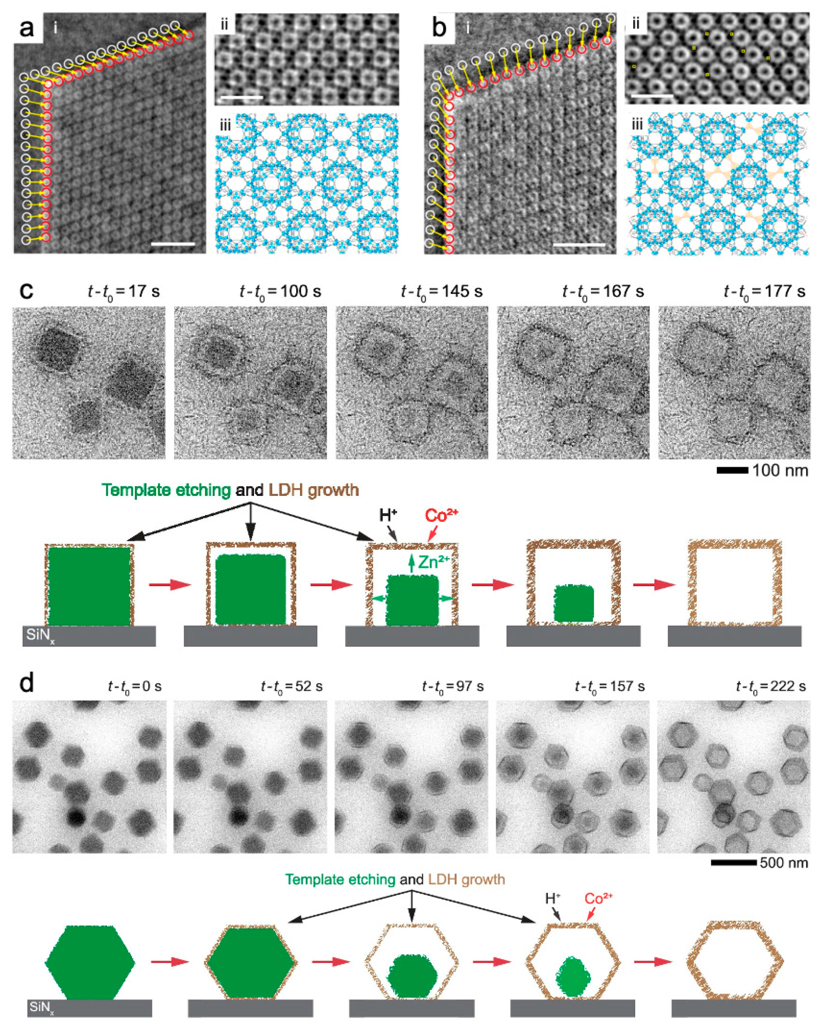
3.3. Traditional STEM and iDPC-STEM
3.4. Dynamic Visualization by In Situ TEM
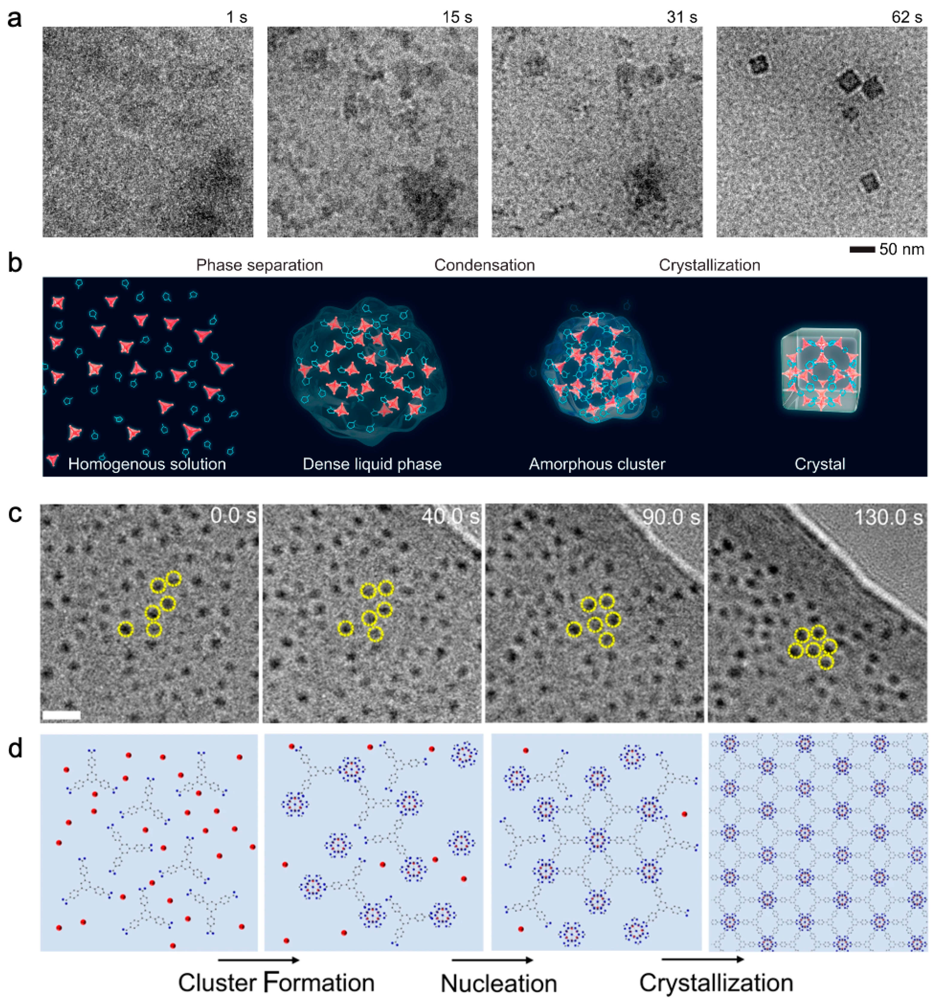
3.4.1. In Situ Synthesis
3.4.2. Phase Transition
3.4.3. Pore Breathing
3.4.4. On Demand Structural Modification
4. Conclusions and Outlook
Author Contributions
Funding
Data Availability Statement
Conflicts of Interest
References
- Furukawa, H.; Cordova, K.E.; O’Keeffe, M.; Yaghi, O.M. The Chemistry and Applications of Metal-Organic Frameworks. Science 2013, 341, 1230444. [Google Scholar] [CrossRef]
- Huang, Y.-B.; Liang, J.; Wang, X.-S.; Cao, R. Multifunctional metal-organic framework catalysts: Synergistic catalysis and tandem reactions. Chem. Soc. Rev. 2017, 46, 126–157. [Google Scholar] [CrossRef]
- Xue, D.-X.; Wang, Q.; Bai, J. Amide-functionalized metal-organic frameworks: Syntheses, structures and improved gas storage and separation properties. Coord. Chem. Rev. 2019, 378, 2–16. [Google Scholar] [CrossRef]
- Adil, K.; Belmabkhout, Y.; Pillai, R.S.; Cadiau, A.; Bhatt, P.M.; Assen, A.H.; Maurin, G.; Eddaoudi, M. Gas/vapour separation using ultra-microporous metal-organic frameworks: Insights into the structure/separation relationship. Chem. Soc. Rev. 2017, 46, 3402–3430. [Google Scholar] [CrossRef]
- Xia, W.; Mahmood, A.; Zou, R.; Xu, Q. Metal-organic frameworks and their derived nanostructures for electrochemical energy storage and conversion. Energy Environ. Sci. 2015, 8, 1837–1866. [Google Scholar] [CrossRef]
- Hu, Z.; Deibert, B.J.; Li, J. Luminescent metal-organic frameworks for chemical sensing and explosive detection. Chem. Soc. Rev. 2014, 43, 5815–5840. [Google Scholar] [CrossRef]
- Furukawa, H.; Gandara, F.; Zhang, Y.-B.; Jiang, J.; Queen, W.L.; Hudson, M.R.; Yaghi, O.M. Water Adsorption in Porous Metal-Organic Frameworks and Related Materials. J. Am. Chem. Soc. 2014, 136, 4369–4381. [Google Scholar] [CrossRef]
- Li, X.X.; Cheng, F.Y.; Zhang, S.N.; Chen, J. Shape-controlled synthesis and lithium-storage study of metal-organic frameworks Zn4O(1,3,5-benzenetribenzoate)(2). J. Power Sources 2006, 160, 542–547. [Google Scholar] [CrossRef]
- Han, X.; Liu, P.; Lin, F.; Chen, W.; Luo, R.; Han, Q.; Jiang, Z.; Wang, X.; Song, S.; Reddy, K.M.; et al. Structures and Structural Evolution of Sublayer Surfaces of Metal-Organic Frameworks. Angew. Chem. Int. Ed. Engl. 2020, 59, 21419–21424. [Google Scholar] [CrossRef]
- Phakatkar, A.H.; Megaridis, C.M.; Shokuhfar, T.; Shahbazian-Yassar, R. Real-time TEM observations of ice formation in graphene liquid cell. Nanoscale 2023, 15, 7006–7013. [Google Scholar] [CrossRef]
- Yanai, N.; Sindoro, M.; Yan, J.; Granick, S. Electric field-induced assembly of monodisperse polyhedral metal-organic framework crystals. J. Am. Chem. Soc. 2013, 135, 34–37. [Google Scholar] [CrossRef] [PubMed]
- Avci, C.; Liu, Y.; Pariente, J.A.; Blanco, A.; Lopez, C.; Imaz, I.; Maspoch, D. Template-Free, Surfactant-Mediated Orientation of Self-Assembled Supercrystals of Metal-Organic Framework Particles. Small 2019, 15, e1902520. [Google Scholar] [CrossRef] [PubMed]
- Bradshaw, D.; Garai, A.; Huo, J. Metal-organic framework growth at functional interfaces: Thin films and composites for diverse applications. Chem. Soc. Rev. 2012, 41, 2344–2381. [Google Scholar] [CrossRef] [PubMed]
- Liu, L.; Chen, Z.; Wang, J.; Zhang, D.; Zhu, Y.; Ling, S.; Huang, K.W.; Belmabkhout, Y.; Adil, K.; Zhang, Y.; et al. Imaging defects and their evolution in a metal-organic framework at sub-unit-cell resolution. Nat. Chem. 2019, 11, 622–628. [Google Scholar] [CrossRef]
- Johnstone, D.N.; Firth, F.C.N.; Grey, C.P.; Midgley, P.A.; Cliffe, M.J.; Collins, S.M. Direct Imaging of Correlated Defect Nanodomains in a Metal-Organic Framework. J. Am. Chem. Soc. 2020, 142, 13081–13089. [Google Scholar] [CrossRef]
- Shi, F.L.; Li, F.; Ma, Y.L.; Zheng, F.Y.; Feng, R.; Song, C.Y.; Tao, P.; Shang, W.; Deng, T.; Wu, J.B. In Situ Transmission Electron Microscopy Study of Nanocrystal Formation for Electrocatalysis. ChemNanoMat 2019, 5, 1439–1455. [Google Scholar] [CrossRef]
- Cliffe, M.J.; Wan, W.; Zou, X.; Chater, P.A.; Kleppe, A.K.; Tucker, M.G.; Wilhelm, H.; Funnell, N.P.; Coudert, F.X.; Goodwin, A.L. Correlated defect nanoregions in a metal-organic framework. Nat. Commun. 2014, 5, 4176. [Google Scholar] [CrossRef]
- Shen, B.; Chen, X.; Shen, K.; Xiong, H.; Wei, F. Imaging the node-linker coordination in the bulk and local structures of metal-organic frameworks. Nat. Commun. 2020, 11, 2692. [Google Scholar] [CrossRef]
- Zahmakiran, M. Iridium nanoparticles stabilized by metal organic frameworks (IrNPs@ZIF-8): Synthesis, structural properties and catalytic performance. Dalton Trans. 2012, 41, 12690–12696. [Google Scholar] [CrossRef]
- Esken, D.; Turner, S.; Lebedev, O.I.; Van Tendeloo, G.; Fischer, R.A. Au@ZIFs: Stabilization and Encapsulation of Cavity-Size Matching Gold Clusters inside Functionalized Zeolite Imidazolate Frameworks, ZIFs. Chem. Mater. 2010, 22, 6393–6401. [Google Scholar] [CrossRef]
- Li, Z.; Wang, G.; Ye, Y.; Li, B.; Li, H.; Chen, B. Loading Photochromic Molecules into a Luminescent Metal-Organic Framework for Information Anticounterfeiting. Angew. Chem. Int. Ed. 2019, 58, 18025–18031. [Google Scholar] [CrossRef]
- Zhang, D.; Zhu, Y.; Liu, L.; Ying, X.; Hsiung, C.E.; Sougrat, R.; Li, K.; Han, Y. Atomic-resolution transmission electron microscopy of electron beam-sensitive crystalline materials. Science 2018, 359, 675–679. [Google Scholar] [CrossRef]
- Jiang, Z.; Xu, X.H.; Ma, Y.H.; Cho, H.S.; Ding, D.; Wang, C.; Wu, J.; Oleynikov, P.; Jia, M.; Cheng, J.; et al. Filling metal-organic framework mesopores with TiO(2)for CO(2)photoreduction. Nature 2020, 586, 549. [Google Scholar] [CrossRef]
- Williams, D.B.; Carter, C.B. Transmission Electron Microscopy: A Textbook for Materials Science; Springer US: Boston, MA, USA, 1996. [Google Scholar]
- Muller, D.A. Structure and bonding at the atomic scale by scanning transmission electron microscopy. Nat. Mater. 2009, 8, 263–270. [Google Scholar] [CrossRef]
- Taheri, M.L.; Stach, E.A.; Arslan, I.; Crozier, P.A.; Kabius, B.C.; LaGrange, T.; Minor, A.M.; Takeda, S.; Tanase, M.; Wagner, J.B.; et al. Current status and future directions for in situ transmission electron microscopy. Ultramicroscopy 2016, 170, 86–95. [Google Scholar] [CrossRef]
- Egerton, R.F. Mechanisms of radiation damage in beam-sensitive specimens, for TEM accelerating voltages between 10 and 300 kV. Microsc. Res. Tech. 2012, 75, 1550–1556. [Google Scholar] [CrossRef]
- Turner, S.; Lebedev, O.I.; Schroder, F.; Esken, D.; Fischer, R.A.; Van Tendeloo, G. Direct imaging of loaded metal-organic framework materials (metal@MOF-5). Chem. Mater. 2008, 20, 5622–5627. [Google Scholar] [CrossRef]
- Wiktor, C.; Turner, S.; Zacher, D.; Fischer, R.A.; Van Tendeloo, G. Imaging of intact MOF-5 nanocrystals by advanced TEM at liquid nitrogen temperature. Microporous Mesoporous Mater. 2012, 162, 131–135. [Google Scholar] [CrossRef]
- Huang, Z.; Willhammar, T.; Zou, X. Three-dimensional electron diffraction for porous crystalline materials: Structural determination and beyond. Chem. Sci. 2021, 12, 1206–1219. [Google Scholar] [CrossRef]
- Li, X.; Mooney, P.; Zheng, S.; Booth, C.R.; Braunfeld, M.B.; Gubbens, S.; Agard, D.A.; Cheng, Y. Electron counting and beam-induced motion correction enable near-atomic-resolution single-particle cryo-EM. Nat. Methods 2013, 10, 584–590. [Google Scholar] [CrossRef]
- Lazic, I.; Bosch, E.G.T.; Lazar, S. Phase contrast STEM for thin samples: Integrated differential phase contrast. Ultramicroscopy 2016, 160, 265–280. [Google Scholar] [CrossRef] [PubMed]
- Huang, Z.; Grape, E.S.; Li, J.; Inge, A.K.; Zou, X. 3D electron diffraction as an important technique for structure elucidation of metal-organic frameworks and covalent organic frameworks. Coord. Chem. Rev. 2021, 427, 213583. [Google Scholar] [CrossRef]
- Yang, T.; Willhammar, T.; Xu, H.; Zou, X.; Huang, Z. Single-crystal structure determination of nanosized metal-organic frameworks by three-dimensional electron diffraction. Nat. Protoc. 2022, 17, 2389–2413. [Google Scholar] [CrossRef] [PubMed]
- Wiktor, C.; Meledina, M.; Turner, S.; Lebedev, O.I.; Fischer, R.A. Transmission electron microscopy on metal-organic frameworks—A review. J. Mater. Chem. A 2017, 5, 14969–14989. [Google Scholar] [CrossRef]
- Liu, L.; Zhang, D.; Zhu, Y.; Han, Y. Bulk and local structures of metal-organic frameworks unravelled by high-resolution electron microscopy. Commun. Chem. 2020, 3, 99. [Google Scholar] [CrossRef]
- Gong, X.; Gnanasekaran, K.; Chen, Z.; Robison, L.; Wasson, M.C.; Bentz, K.C.; Cohen, S.M.; Farha, O.K.; Gianneschi, N.C. Insights into the Structure and Dynamics of Metal-Organic Frameworks via Transmission Electron Microscopy. J. Am. Chem. Soc. 2020, 142, 17224–17235. [Google Scholar] [CrossRef]
- Zhang, J.; Cheng, N.; Ge, B. Characterization of metal-organic frameworks by transmission electron microscopy. Adv. Phys. X 2022, 7, 2046157. [Google Scholar] [CrossRef]
- Egerton, R.F.; Li, P.; Malac, M. Radiation damage in the TEM and SEM. Micron 2004, 35, 399–409. [Google Scholar] [CrossRef]
- Diaz-Garcia, M.; Mayoral, A.; Diaz, I.; Sanchez-Sanchez, M. Nanoscaled M-MOF-74 Materials Prepared at Room Temperature. Cryst. Growth Des. 2014, 14, 2479–2487. [Google Scholar] [CrossRef]
- Lebedev, O.I.; Millange, F.; Serre, C.; Van Tendeloo, G.; Ferey, G. First direct imaging of giant pores of the metal-organic framework MIL-101. Chem. Mater. 2005, 17, 6525–6527. [Google Scholar] [CrossRef]
- Li, X.; Wang, J.; Liu, X.; Liu, L.; Cha, D.; Zheng, X.; Yousef, A.A.; Song, K.; Zhu, Y.; Zhang, D.; et al. Direct Imaging of Tunable Crystal Surface Structures of MOF MIL-101 Using High-Resolution Electron Microscopy. J. Am. Chem. Soc. 2019, 141, 12021–12028. [Google Scholar] [CrossRef]
- Zhu, Y.; Ciston, J.; Zheng, B.; Miao, X.; Czarnik, C.; Pan, Y.; Sougrat, R.; Lai, Z.; Hsiung, C.E.; Yao, K.; et al. Unravelling surface and interfacial structures of a metal-organic framework by transmission electron microscopy. Nat. Mater. 2017, 16, 532–536. [Google Scholar] [CrossRef]
- Patterson, J.P.; Abellan, P.; Denny, M.S., Jr.; Park, C.; Browning, N.D.; Cohen, S.M.; Evans, J.E.; Gianneschi, N.C. Observing the growth of metal-organic frameworks by in situ liquid cell transmission electron microscopy. J. Am. Chem. Soc. 2015, 137, 7322–7328. [Google Scholar] [CrossRef]
- Liu, Y.; Wei, Y.; Liu, M.; Bai, Y.; Wang, X.; Shang, S.; Du, C.; Gao, W.; Chen, J.; Liu, Y. Face-to-Face Growth of Wafer-Scale 2D Semiconducting MOF Films on Dielectric Substrates. Adv. Mater. 2021, 33, 2007741. [Google Scholar] [CrossRef]
- Feyand, M.; Mugnaioli, E.; Vermoortele, F.; Bueken, B.; Dieterich, J.M.; Reimer, T.; Kolb, U.; de Vos, D.; Stock, N. Automated diffraction tomography for the structure elucidation of twinned, sub-micrometer crystals of a highly porous, catalytically active bismuth metal-organic framework. Angew. Chem. Int. Ed. Engl. 2012, 51, 10373–10376. [Google Scholar] [CrossRef]
- Liu, X.; Chee, S.W.; Raj, S.; Sawczyk, M.; Kral, P.; Mirsaidov, U. Three-step nucleation of metal-organic framework nanocrystals. Proc. Natl. Acad. Sci. USA 2021, 118, e2008880118. [Google Scholar] [CrossRef]
- Peng, X.; Pelz, P.M.; Zhang, Q.; Chen, P.; Cao, L.; Zhang, Y.; Liao, H.-G.; Zheng, H.; Wang, C.; Sun, S.-G.; et al. Observation of formation and local structures of metal-organic layers via complementary electron microscopy techniques. Nat. Commun. 2022, 13, 5197. [Google Scholar] [CrossRef]
- Li, Y.Z.; Wang, K.C.; Zhou, W.J.; Li, Y.B.; Vila, R.; Huang, W.; Wang, H.X.; Chen, G.X.; Wu, G.H.; Tsao, Y.C.; et al. Cryo-EM Structures of Atomic Surfaces and Host-Guest Chemistry in Metal-Organic Frameworks. Matter 2019, 1, 428–438. [Google Scholar] [CrossRef]
- Ogata, A.F.; Rakowski, A.M.; Carpenter, B.P.; Fishman, D.A.; Merham, J.G.; Hurst, P.J.; Patterson, J.P. Direct Observation of Amorphous Precursor Phases in the Nucleation of Protein-Metal-Organic Frameworks. J. Am. Chem. Soc. 2020, 142, 1433–1442. [Google Scholar] [CrossRef]
- Tong, L.; Huang, S.; Shen, Y.; Liu, S.; Ma, X.; Zhu, F.; Chen, G.; Ouyang, G. Atomically unveiling the structure-activity relationship of biomacromolecule-metal-organic frameworks symbiotic crystal. Nat. Commun. 2022, 13, 951. [Google Scholar] [CrossRef]
- Zhu, L.K.; Zhang, D.L.; Xue, M.; Li, H.; Qiu, S.L. Direct observations of the MOF (UiO-66) structure by transmission electron microscopy. Crystengcomm 2013, 15, 9356–9359. [Google Scholar] [CrossRef]
- Gemmi, M.; Mugnaioli, E.; Gorelik, T.E.; Kolb, U.; Palatinus, L.; Boullay, P.; Hovmoller, S.; Abrahams, J.P. 3D Electron Diffraction: The Nanocrystallography Revolution. ACS Cent. Sci. 2019, 5, 1315–1329. [Google Scholar] [CrossRef]
- Kolb, U.; Gorelik, T.; Kubel, C.; Otten, M.T.; Hubert, D. Towards automated diffraction tomography: Part I—Data acquisition. Ultramicroscopy 2007, 107, 507–513. [Google Scholar] [CrossRef]
- Kolb, U.; Gorelik, T.; Otten, M.T. Towards automated diffraction tomography. Part II—Cell parameter determination. Ultramicroscopy 2008, 108, 763–772. [Google Scholar] [CrossRef]
- Denysenko, D.; Grzywa, M.; Tonigold, M.; Streppel, B.; Krkljus, I.; Hirscher, M.; Mugnaioli, E.; Kolb, U.; Hanss, J.; Volkmer, D. Elucidating Gating Effects for Hydrogen Sorption in MFU-4-Type Triazolate-Based Metal-Organic Frameworks Featuring Different Pore Sizes. Chem. A Eur. J. 2011, 17, 1837–1848. [Google Scholar] [CrossRef]
- Wan, W.; Sun, J.; Su, J.; Hovmoller, S.; Zou, X. Three-dimensional rotation electron diffraction: Software RED for automated data collection and data processing. J. Appl. Crystallogr. 2013, 46, 1863–1873. [Google Scholar] [CrossRef]
- Yuan, S.; Qin, J.-S.; Xu, H.-Q.; Su, J.; Rossi, D.; Chen, Y.; Zhang, L.; Lollar, C.; Wang, Q.; Jiang, H.-L.; et al. Ti8Zr2O12(COO)(16) Cluster: An Ideal Inorganic Building Unit for Photoactive Metal-Organic Frameworks. ACS Cent. Sci. 2018, 4, 105–111. [Google Scholar] [CrossRef]
- Smolders, S.; Willhammar, T.; Krajnc, A.; Sentosun, K.; Wharmby, M.T.; Lomachenko, K.A.; Bals, S.; Mali, G.; Roeffaers, M.B.J.; De Vos, D.E.; et al. A Titanium(IV)-Based Metal-Organic Framework Featuring Defect-Rich Ti-O Sheets as an Oxidative Desulfurization Catalyst. Angew. Chem. Int. Ed. 2019, 58, 9160–9165. [Google Scholar] [CrossRef]
- Cichocka, M.O.; Liang, Z.; Feng, D.; Back, S.; Siahrostami, S.; Wang, X.; Samperisi, L.; Sun, Y.; Xu, H.; Hedin, N.; et al. A Porphyrinic Zirconium Metal-Organic Framework for Oxygen Reduction Reaction: Tailoring the Spacing between Active-Sites through Chain-Based Inorganic Building Units. J. Am. Chem. Soc. 2020, 142, 15386–15395. [Google Scholar] [CrossRef]
- Ge, M.; Yang, T.; Wang, Y.; Carraro, F.; Liang, W.; Doonan, C.; Falcaro, P.; Zheng, H.; Zou, X.; Huang, Z. On the completeness of three-dimensional electron diffraction data for structural analysis of metal-organic frameworks. Faraday Discuss. 2021, 231, 66–80. [Google Scholar] [CrossRef]
- Roy, S.; Huang, Z.; Bhunia, A.; Castner, A.; Gupta, A.K.; Zou, X.; Ott, S. Electrocatalytic Hydrogen Evolution from a Cobaloxime-Based Metal-Organic Framework Thin Film. J. Am. Chem. Soc. 2019, 141, 15942–15950. [Google Scholar] [CrossRef]
- Xie, L.S.; Skorupskii, G.; Dinca, M. Electrically Conductive Metal-Organic Frameworks. Chem. Rev. 2020, 120, 8536–8580. [Google Scholar] [CrossRef]
- Dou, J.-H.; Arguilla, M.Q.; Luo, Y.; Li, J.; Zhang, W.; Sun, L.; Mancuso, J.L.; Yang, L.; Chen, T.; Parent, L.R.; et al. Atomically precise single-crystal structures of electrically conducting 2D metal-organic frameworks. Nat. Mater. 2021, 20, 222. [Google Scholar] [CrossRef]
- Cichocka, M.O.; Angstrom, J.; Wang, B.; Zou, X.; Smeets, S. High-throughput continuous rotation electron diffraction data acquisition via software automation. J. Appl. Crystallogr. 2018, 51, 1652–1661. [Google Scholar] [CrossRef]
- Nannenga, B.L.; Shi, D.; Leslie, A.G.W.; Gonen, T. High-resolution structure determination by continuous-rotation data collection in MicroED. Nat. Methods 2014, 11, 927–930. [Google Scholar] [CrossRef]
- Shi, D.; Nannenga, B.L.; Iadanza, M.G.; Gonen, T. Three-dimensional electron crystallography of protein microcrystals. eLife 2013, 2, e01345. [Google Scholar] [CrossRef]
- Banihashemi, F.; Bu, G.; Thaker, A.; Williams, D.; Lin, J.Y.S.; Nannenga, B.L. Beam-sensitive metal-organic framework structure determination by microcrystal electron diffraction. Ultramicroscopy 2020, 216, 113048. [Google Scholar] [CrossRef]
- Ling, Y.; Sun, T.; Guo, L.; Si, X.; Jiang, Y.; Zhang, Q.; Chen, Z.; Terasaki, O.; Ma, Y. Atomic-level structural responsiveness to environmental conditions from 3D electron diffraction. Nat. Commun. 2022, 13, 6625. [Google Scholar] [CrossRef]
- Wang, B.; Rhauderwiek, T.; Inge, A.K.; Xu, H.; Yang, T.; Huang, Z.; Stock, N.; Zou, X. A Porous Cobalt Tetraphosphonate Metal-Organic Framework: Accurate Structure and Guest Molecule Location Determined by Continuous-Rotation Electron Diffraction. Chem. A Eur. J. 2018, 24, 17429–17433. [Google Scholar] [CrossRef]
- Hynek, J.; Brazda, P.; Rohlicek, J.; Londesborough, M.G.S.; Demel, J. Phosphinic Acid Based Linkers: Building Blocks in Metal-Organic Framework Chemistry. Angew. Chem. Int. Ed. Engl. 2018, 57, 5016–5019. [Google Scholar] [CrossRef]
- Nellist, P.D.; Chisholm, M.F.; Dellby, N.; Krivanek, O.L.; Murfitt, M.F.; Szilagyi, Z.S.; Lupini, A.R.; Borisevich, A.; Sides, W.H., Jr.; Pennycook, S.J. Direct sub-angstrom imaging of a crystal lattice. Science 2004, 305, 1741. [Google Scholar] [CrossRef]
- Vailonis, K.M.; Gnanasekaran, K.; Powers, X.B.; Gianneschi, N.C.; Jenkins, D.M. Elucidating the Growth of Metal-Organic Nanotubes Combining Isoreticular Synthesis with Liquid-Cell Transmission Electron Microscopy. J. Am. Chem. Soc. 2019, 141, 10177–10182. [Google Scholar] [CrossRef]
- Stevens, A.; Luzi, L.; Yang, H.; Kovarik, L.; Mehdi, B.L.; Liyu, A.; Gehm, M.E.; Browning, N.D. A sub-sampled approach to extremely low-dose STEM. Appl. Phys. Lett. 2018, 112, 043104. [Google Scholar] [CrossRef]
- Shen, K.; Zhang, L.; Chen, X.; Liu, L.; Zhang, D.; Han, Y.; Chen, J.; Long, J.; Luque, R.; Li, Y.; et al. Ordered macro-microporous metal-organic framework single crystals. Science 2018, 359, 206–210. [Google Scholar] [CrossRef]
- Wei, J.; Cheng, N.; Liang, Z.; Wu, Y.; Zou, Z.; Zhuang, Z.; Yu, Y. Heterometallic metal–organic framework nanocages of high crystallinity: An elongated channel structure formed in situ through metal-ion (M = W or Mo) doping. J. Mater. Chem. A 2018, 6, 23336–23344. [Google Scholar] [CrossRef]
- Aulakh, D.; Liu, L.; Varghese, J.R.; Xie, H.; Islamoglu, T.; Duell, K.; Kung, C.W.; Hsiung, C.E.; Zhang, Y.; Drout, R.J.; et al. Direct Imaging of Isolated Single-Molecule Magnets in Metal-Organic Frameworks. J. Am. Chem. Soc. 2019, 141, 2997–3005. [Google Scholar] [CrossRef]
- Muller, M.; Hermes, S.; Kaehler, K.; van den Berg, M.W.E.; Muhler, M.; Fischer, R.A. Loading of MOF-5 with Cu and ZnO nanoparticles by gas-phase infiltration with organometallic precursors: Properties of Cu/ZnO@MOF-5 as catalyst for methanol synthesis. Chem. Mater. 2008, 20, 4576–4587. [Google Scholar] [CrossRef]
- Proch, S.; Herrmannsdorfer, J.; Kempe, R.; Kern, C.; Jess, A.; Seyfarth, L.; Senker, J. Pt@MOF-177: Synthesis, Room-Temperature Hydrogen Storage and Oxidation Catalysis. Chem. Eur. J. 2008, 14, 8204–8212. [Google Scholar] [CrossRef]
- Hermannsdorfer, J.; Kempe, R. Selective palladium-loaded MIL-101 catalysts. Chemistry 2011, 17, 8071–8077. [Google Scholar] [CrossRef]
- Li, G.; Kobayashi, H.; Taylor, J.M.; Ikeda, R.; Kubota, Y.; Kato, K.; Takata, M.; Yamamoto, T.; Toh, S.; Matsumura, S.; et al. Hydrogen storage in Pd nanocrystals covered with a metal-organic framework. Nat. Mater. 2014, 13, 802–806. [Google Scholar] [CrossRef]
- Ghosh, S.; Yun, H.; Kumar, P.; Conrad, S.; Tsapatsis, M.; Mkhoyan, K.A. Two Distinct Stages of Structural Modification of ZIF-L MOF under Electron-Beam Irradiation. Chem. Mater. 2021, 33, 5681–5689. [Google Scholar] [CrossRef]
- Meledina, M.; Turner, S.; Filippousi, M.; Leus, K.; Lobato, I.; Ramachandran, R.K.; Dendooven, J.; Detavernier, C.; Van der Voort, P.; Van Tendeloo, G. Direct Imaging of ALD Deposited Pt Nanoclusters inside the Giant Pores of MIL-101. Part. Part. Syst. Charact. 2016, 33, 382–387. [Google Scholar] [CrossRef]
- Mayoral, A.; Sanchez-Sanchez, M.; Alfayate, A.; Perez-Pariente, J.; Diaz, I. Atomic Observations of Microporous Materials Highly Unstable under the Electron Beam: The Cases of Ti-Doped AlPO4-5 and Zn-MOF-74. ChemCatChem 2015, 7, 3719–3724. [Google Scholar] [CrossRef]
- Cha, J.H.; Noh, K.; Yin, W.; Lee, Y.; Park, Y.; Ahn, T.K.; Mayoral, A.; Kim, J.; Jung, D.Y.; Terasaki, O. Formation and Encapsulation of All-Inorganic Lead Halide Perovskites at Room Temperature in Metal-Organic Frameworks. J. Phys. Chem. Lett. 2019, 10, 2270–2277. [Google Scholar] [CrossRef]
- Zhou, Y.; Xu, X.H.; Carlsson, A.; Lazar, S.; Pan, Z.C.; Ma, Y.H.; Terasaki, O.; Deng, H.X. Local Structure Evolvement in MOF Single Crystals Unveiled by Scanning Transmission Electron Microscopy. Chem. Mater. 2020, 32, 4966–4972. [Google Scholar] [CrossRef]
- Liu, B.; Chen, X.; Huang, N.; Liu, S.; Shen, B.; Wei, F.; Wang, T. Interaction between Single Metal Atoms and UiO-66 Framework Revealed by Low-Dose Imaging. Nano Lett. 2023, 23, 1787–1793. [Google Scholar] [CrossRef]
- Chaupard, M.; Degrouard, J.; Li, X.; Stephan, O.; Kociak, M.; Gref, R.; de Frutos, M. Nanoscale Multimodal Analysis of Sensitive Nanomaterials by Monochromated STEM-EELS in Low-Dose and Cryogenic Conditions. ACS Nano 2023, 17, 3452–3464. [Google Scholar] [CrossRef]
- Gnanasekaran, K.; Vailonis, K.M.; Jenkins, D.M.; Gianneschi, N.C. In Situ Monitoring of the Seeding and Growth of Silver Metal-Organic Nanotubes by Liquid-Cell Transmission Electron Microscopy. ACS Nano 2020, 14, 8735–8743. [Google Scholar] [CrossRef]
- Lyu, J.; Gong, X.; Lee, S.-J.; Gnanasekaran, K.; Zhang, X.; Wasson, M.C.; Wang, X.; Bai, P.; Guo, X.; Gianneschi, N.C.; et al. Phase Transitions in Metal-Organic Frameworks Directly Monitored through In Situ Variable Temperature Liquid-Cell Transmission Electron Microscopy and In Situ X-ray Diffraction. J. Am. Chem. Soc. 2020, 142, 4609–4615. [Google Scholar] [CrossRef]
- Parent, L.R.; Pham, C.H.; Patterson, J.P.; Denny, M.S., Jr.; Cohen, S.M.; Gianneschi, N.C.; Paesani, F. Pore Breathing of Metal-Organic Frameworks by Environmental Transmission Electron Microscopy. J. Am. Chem. Soc. 2017, 139, 13973–13976. [Google Scholar] [CrossRef]
- Ishikawa, R.; Okunishi, E.; Sawada, H.; Kondo, Y.; Hosokawa, F.; Abe, E. Direct imaging of hydrogen-atom columns in a crystal by annular bright-field electron microscopy. Nat. Mater. 2011, 10, 278–281. [Google Scholar] [CrossRef] [PubMed]
- Nellist, P.D.; Pennycook, S.J. Incoherent imaging using dynamically scattered coherent electrons. Ultramicroscopy 1999, 78, 111–124. [Google Scholar] [CrossRef]
- Thiam, Z.; Abou-Hamad, E.; Dereli, B.; Liu, L.; Emwas, A.H.; Ahmad, R.; Jiang, H.; Isah, A.A.; Ndiaye, P.B.; Taoufik, M.; et al. Extension of Surface Organometallic Chemistry to Metal-Organic Frameworks: Development of a Well-Defined Single Site [(identical withZr-O-)W(horizontal lineO)(CH2(t)Bu)3] Olefin Metathesis Catalyst. J. Am. Chem. Soc. 2020, 142, 16690–16703. [Google Scholar] [CrossRef] [PubMed]
- Sha, H.; Cui, J.; Yu, R. Deep sub-angstrom resolution imaging by electron ptychography with misorientation correction. Sci. Adv. 2022, 8, eabn2275. [Google Scholar] [CrossRef]
- Yucelen, E.; Lazic, I.; Bosch, E.G.T. Phase contrast scanning transmission electron microscopy imaging of light and heavy atoms at the limit of contrast and resolution. Sci. Rep. 2018, 8, 2676. [Google Scholar] [CrossRef]
- Sun, D.; Wong, L.W.; Wong, H.Y.; Lai, K.H.; Ye, L.; Xv, X.; Ly, T.H.; Deng, Q.; Zhao, J. Direct Visualization of Atomic Structure in Multivariate Metal-Organic Frameworks (MOFs) for Guiding Electrocatalysts Design. Angew. Chem. Int. Ed. 2022, 135, e202216008. [Google Scholar] [CrossRef]
- Denny, M.S., Jr.; Parent, L.R.; Patterson, J.P.; Meena, S.K.; Pham, H.; Abellan, P.; Ramasse, Q.M.; Paesani, F.; Gianneschi, N.C.; Cohen, S.M. Transmission Electron Microscopy Reveals Deposition of Metal Oxide Coatings onto Metal-Organic Frameworks. J. Am. Chem. Soc. 2018, 140, 1348–1357. [Google Scholar] [CrossRef]
- Xing, J.; Schweighauser, L.; Okada, S.; Harano, K.; Nakamura, E. Atomistic structures and dynamics of prenucleation clusters in MOF-2 and MOF-5 syntheses. Nat. Commun. 2019, 10, 3608. [Google Scholar] [CrossRef]
- Li, H.; Wang, K.C.; Sun, Y.J.; Lollar, C.T.; Li, J.L.; Zhou, H.C. Recent advances in gas storage and separation using metal-organic frameworks. Mater. Today 2018, 21, 108–121. [Google Scholar] [CrossRef]
- Li, Y.; Yang, R.T. Gas adsorption and storage in metal-organic framework MOF-177. Langmuir 2007, 23, 12937–12944. [Google Scholar] [CrossRef]
- Wang, W.; Yan, H.; Anand, U.; Mirsaidov, U. Visualizing the Conversion of Metal-Organic Framework Nanoparticles into Hollow Layered Double Hydroxide Nanocages. J. Am. Chem. Soc. 2021, 143, 1854–1862. [Google Scholar] [CrossRef]
- Houk, R.J.T.; Jacobs, B.W.; El Gabaly, F.; Chang, N.N.; Talin, A.A.; Graham, D.D.; House, S.D.; Robertson, I.M.; Allendorf, M.D. Silver Cluster Formation, Dynamics, and Chemistry in Metal-Organic Frameworks. Nano Lett. 2009, 9, 3413–3418. [Google Scholar] [CrossRef]
- Mezenov, Y.A.; Bruyere, S.; Kulachenkov, N.K.; Yankin, A.N.; Rzhevskiy, S.S.; Alekseevskiy, P.V.; Gilemkhanova, V.D.; Bachinin, S.V.; Dyachuk, V.; Krasilin, A.A.; et al. Probing the dynamics of Cu nanoparticle growth inside metal-organic frameworks upon electron beam irradiation. Photonics Nanostruct. Fundam. Appl. 2020, 41, 100832. [Google Scholar] [CrossRef]
- Xu, D.; Zhang, D.; Zou, H.; Zhu, L.; Xue, M.; Fang, Q.; Qiu, S. Guidance from an in situ hot stage in TEM to synthesize magnetic metal nanoparticles from a MOF. Chem. Commun. 2016, 52, 10513–10516. [Google Scholar] [CrossRef]
- Wang, Z.; Ke, X.; Zhou, K.; Xu, X.; Jin, Y.; Wang, H.; Sui, M. Engineering the structure of ZIF-derived catalysts by revealing the critical role of temperature for enhanced oxygen reduction reaction. J. Mater. Chem. A 2021, 9, 18515–18525. [Google Scholar] [CrossRef]
- Zhou, Y.; Deng, X.; Xing, H.; Zhao, H.; Liu, Y.; Guo, L.; Feng, J.; Feng, W.; Zong, Y.; Zhu, X.; et al. Dynamically observing the formation of MOFs-driven Co/N-doped carbon nanocomposites by in-situ transmission electron microscope and their application as high-efficient microwave absorbent. Nano Res. 2022, 15, 6819–6830. [Google Scholar] [CrossRef]
- Ercius, P.; Alaidi, O.; Rames, M.J.; Ren, G. Electron Tomography: A Three-Dimensional Analytic Tool for Hard and Soft Materials Research. Adv. Mater. 2015, 27, 5638–5663. [Google Scholar] [CrossRef]
- Ophus, C. Four-Dimensional Scanning Transmission Electron Microscopy (4D-STEM): From Scanning Nanodiffraction to Ptychography and Beyond. Microsc. Microanal. 2019, 25, 563–582. [Google Scholar] [CrossRef]
- Zhang, D.; Wei, N.; Liu, L.; Song, K.; Behzad, A.; Genovese, A.; Han, Y. Cryo Focused Ion Beam Applications in High Resolution Electron Microscopy Studies of Beam Sensitive Crystals. Microsc. Microanal. 2019, 25, 1402–1403. [Google Scholar] [CrossRef]
- Rivas, N.A.; Babayigit, A.; Conings, B.; Schwarz, T.; Sturm, A.; Manjon, A.G.; Cojocaru-Miredin, O.; Gault, B.; Renner, F.U. Cryo-focused ion beam preparation of perovskite based solar cells for atom probe tomography. PLoS ONE 2020, 15, e0227920. [Google Scholar] [CrossRef]
- Sha, H.; Cui, J.; Li, J.; Zhang, Y.; Yang, W.; Li, Y.; Yu, R. Ptychographic measurements of varying size and shape along zeolite channels. Sci. Adv. 2023, 9, eadf1151. [Google Scholar] [CrossRef] [PubMed]
- Zhang, H.; Li, G.; Zhang, J.; Zhang, D.; Chen, Z.; Liu, X.; Guo, P.; Zhu, Y.; Chen, C.; Liu, L.; et al. Three-dimensional inhomogeneity of zeolite structure and composition revealed by electron ptychography. Science 2023, 380, 633–638. [Google Scholar] [CrossRef] [PubMed]


| Imaging Techniques | Advanced Cameras | Materials | Accelerating Voltage | Temperature | Damage Threshold of Electron Dose | Cumulative Electron Dose for Imaging | Spatial Resolution | Imaged Structures | Reference | Year |
|---|---|---|---|---|---|---|---|---|---|---|
| HRTEM | MOF-5(Zn) | 80 kV | Cryo (liquid nitrogen temperature) | Surface | [29] | 2012 | ||||
| HRTEM | 2D Cu2(TCPP) film | 80 kV | Cryo | Bulk | [45] | 2021 | ||||
| HRTEM | DDEC camera | ZIF-8(Zn) | 300 kV | ~25 e− Å−2 | 4.1 e− Å−2 | 2.1 Å | Bulk, surface, interface | [43] | 2017 | |
| HRTEM | DDEC camera | ZIF-8 | 300 kV | ~5 e− Å−2 | Bulk | [22] | 2018 | |||
| HRTEM | DDEC camera | ZIF-8(Zn) | 300 kV | Bulk | [75] | 2018 | ||||
| HRTEM | DDEC camera | ZIF-8(Zn), CO2@ZIF-8(Zn) | 300 kV | Cryo (~103 K) | ~50 e− Å−2 | ~7 e− Å−2 | Bulk, surface, host–guest interactions | [49] | 2019 | |
| HRTEM | DDEC camera | protein-ZIF-8(Zn) | 200 kV | Cryo | 1 e− Å−2 s−1 dose rate and 5 s exposure time) | Nucleation, growth | [50] | 2020 | ||
| HRTEM | DDEC camera | MIL-101(Cr) | 300 kV | ~16 e− Å−2 | ~8 e− Å−2 | 2.5 Å | Bulk, surface | [42] | 2019 | |
| HRTEM | DDEC camera | MIL-101(Cr) | 200 kV | 22–32 e− Å−2 | 10 e− Å−2 | Bulk, sublayer surface, surface | [9] | 2020 | ||
| HRTEM | DDEC camera | UiO-66(Zr) | 300 kV | 10–20 e− Å−2 | ~12 e− Å−2 | Bulk, surface | [22] | 2018 | ||
| HRTEM | DDEC camera | UiO-66(Zr) | 300 kV | Surface, defects | [14] | 2019 | ||||
| HRTEM | DDEC camera | HKUST-1 | 300 kV | ~6 e− Å−2 | Bulk | [22] | 2018 | |||
| HRTEM | DDEC camera | W doped UiO-66(Zr) | 200 kV | 5–10 e− Å−2 | Bulk | [76] | 2018 | |||
| HRTEM | DDEC camera | Mn12Ac@NU-1000(Zr) | 300 kV | Bulk, host–guest interactions | [77] | 2019 | ||||
| HRTEM | DDEC camera | ZIF-L(Zn) | 300 kV | ~26 e− Å−2 | Structural modification | [82] | 2021 | |||
| ADF-STEM | MIL-101(Cr), Pt@MIL-101(Cr) | 200 kV | Bulk, surface, host–guest interactions | [83] | 2016 | |||||
| HAADF-STEM | MIL-101(Cr), TiO2-in-MIL-101(Cr) composites | 300 kV | 3.9 Å, 5.2 Å | Bulk, surface, host–guest interactions | [23] | 2020 | ||||
| HAADF-STEM | MOF-74(Zn) | 300 kV | Bulk | [40] | 2014 | |||||
| HAADF-STEM | MOF-74(Zn) | 300 kV | 2.9 Å | Bulk, surface | [84] | 2015 | ||||
| HAADF-STEM | CsPbI3@ MIL-101(Cr) | 300 kV | Bulk, surface, host–guest interactions | [85] | 2019 | |||||
| HAADF-STEM | MIL-101(Cr) | 300 kV | 54 e− Å−2 | 4.7 Å | Bulk, surface | [86] | 2020 | |||
| HAADF-STEM | ZIF-L(Zn) | 200 kV | ~25 e− Å−2 | Structural modification | [82] | 2021 | ||||
| HAADF-STEM | 2D Hf-MOFs | 300 kV | 106 e− Å−2 | Bulk, surface, interface, defects | [48] | 2022 | ||||
| iDPC-STEM | MIL-101(Cr) | 300 kV | ~35 e− Å−2 | Surface | [42] | 2019 | ||||
| iDPC-STEM | MIL-101(Cr) | 300 kV | <40 e− Å−2 | 1.8 Å | Bulk, surface, interface, defects, nodes and linkers | [18] | 2020 | |||
| iDPC-STEM | MIL-101(Cr), TiO2-in-MIL-101(Cr) composites | 300 kV | 3.2 Å, 3.1 Å | Bulk, surface, host–guest interactions | [23] | 2020 | ||||
| iDPC-STEM | MIL-101(Cr) | 300 kV | 54 e− Å−2 | 4.7 Å | Bulk, surface | [86] | 2020 | |||
| iDPC-STEM | protein-ZIF-8(Zn) | 300 kV | Cryo | 30 e− Å−2 | Bulk, nucleation, growth | [51] | 2022 | |||
| iDPC-STEM | Pt@UiO-66(Zr), Pd@UiO-66(Zr) | 300 kV | ~4.7 Å | Bulk, host–guest interactions | [87] | 2023 | ||||
| STEM-EELS | DDEC camera | MIL-100(Al), MIL-100(Fe), UiO-66(Zr) | 100 kV | Cryo (125 K) | 10 e− Å−2 | 10 nm (energy resolution: 7 meV) | Chemical information | [88] | 2023 | |
| In situ TEM: liquid cell | ZIF-8(Zn) | 200 kV, 300 kV | ~4000 e− nm−2 | Nucleation, growth | [44] | 2015 | ||||
| In situ TEM: liquid cell | DDEC camera | ZIF-8(Zn) | 200 kV | 5 e− Å−2 | Nucleation, growth | [47] | 2021 | |||
| In situ TEM: liquid cell, heating | Advanced scintillator-based camera | 1D [(L1)Cu2Br2] MOFs | 300 kV | Room temperature (23 °C), heating (85 °C) | <10 e− Å−2 | Nucleation, growth | [73] | 2019 | ||
| In situ TEM: liquid cell | DDEC camera, advanced scintillator-based camera | 1D Ag-MOFs | 300 kV | 70 e− Å−2 | Nucleation, growth | [89] | 2020 | |||
| In situ TEM: liquid cell, heating | DDEC camera, advanced scintillator-based camera | NU-906, NU-1008 | 300 kV | Room temperature, heating (80 °C) | <6 e− Å−2 | Bulk, phase transition | [90] | 2020 | ||
| In situ TEM: ETEM (gas) | Advanced scintillator-based camera | H2O@MIL-53(Cr) | 300 kV | Room temperature (27 °C), heating (800 °C) | ~5 e− Å−2 | Pore breathing | [91] | 2017 |
Disclaimer/Publisher’s Note: The statements, opinions and data contained in all publications are solely those of the individual author(s) and contributor(s) and not of MDPI and/or the editor(s). MDPI and/or the editor(s) disclaim responsibility for any injury to people or property resulting from any ideas, methods, instructions or products referred to in the content. |
© 2023 by the authors. Licensee MDPI, Basel, Switzerland. This article is an open access article distributed under the terms and conditions of the Creative Commons Attribution (CC BY) license (https://creativecommons.org/licenses/by/4.0/).
Share and Cite
Zheng, A.; Yin, K.; Pan, R.; Zhu, M.; Xiong, Y.; Sun, L. Research Progress on Metal–Organic Frameworks by Advanced Transmission Electron Microscopy. Nanomaterials 2023, 13, 1742. https://doi.org/10.3390/nano13111742
Zheng A, Yin K, Pan R, Zhu M, Xiong Y, Sun L. Research Progress on Metal–Organic Frameworks by Advanced Transmission Electron Microscopy. Nanomaterials. 2023; 13(11):1742. https://doi.org/10.3390/nano13111742
Chicago/Turabian StyleZheng, Anqi, Kuibo Yin, Rui Pan, Mingyun Zhu, Yuwei Xiong, and Litao Sun. 2023. "Research Progress on Metal–Organic Frameworks by Advanced Transmission Electron Microscopy" Nanomaterials 13, no. 11: 1742. https://doi.org/10.3390/nano13111742
APA StyleZheng, A., Yin, K., Pan, R., Zhu, M., Xiong, Y., & Sun, L. (2023). Research Progress on Metal–Organic Frameworks by Advanced Transmission Electron Microscopy. Nanomaterials, 13(11), 1742. https://doi.org/10.3390/nano13111742