Article

Ultra-Narrowband Anisotropic Perfect Absorber Based on α-MoO3 Metamaterials in the Visible Light Region

1
Department of Electronic Information and Electronic Engineering, Xiangnan University, Chenzhou 423000, China
2
School of Microelectronics and Control Engineering, Changzhou University, Changzhou 213163, China
*
Author to whom correspondence should be addressed.
Nanomaterials 2022, 12(8), 1375; https://doi.org/10.3390/nano12081375
Submission received: 21 March 2022 / Revised: 13 April 2022 / Accepted: 15 April 2022 / Published: 17 April 2022
(This article belongs to the Topic Advances and Applications of 2D Materials)

Abstract

:
Optically anisotropic materials show important advantages in constructing polarization-dependent optical devices. Very recently, a new type of two-dimensional van der Waals (vdW) material, known as α-phase molybdenum trioxide (α-MoO3), has sparked considerable interest owing to its highly anisotropic characteristics. In this work, we theoretically present an anisotropic metamaterial absorber composed of α-MoO3 rings and dielectric layer stacking on a metallic mirror. The designed absorber can exhibit ultra-narrowband perfect absorption for polarizations along [100] and [001] crystalline directions in the visible light region. Plus, the influences of some geometric parameters on the optical absorption spectra are discussed. Meanwhile, the proposed ultra-narrowband anisotropic perfect absorber has an excellent angular tolerance for the case of oblique incidence. Interestingly, the single-band perfect absorption in our proposed metamaterials can be arbitrarily extended to multi-band perfect absorption by adjusting the thickness of dielectric layer. The physical mechanism can be explained by the interference theory in Fabry–Pérot cavity, which is consistent with the numerical simulation. Our research results have some potential applications in designs of anisotropic optical devices with tunable spectrum and selective polarization in the visible light region.

1. Introduction

Two-dimensional (2D) materials with atomic-scale thicknesses, i.e., graphene [1], black phosphorus (BP) [2], hexagonal boron nitride (h-BN) [3], and transition metal dichalcogenides (TMDs) [4], have been much concerned due to their distinctive optical and electrical properties over the past few years [5]. Different from the optoelectronic devices made of conventional bulk materials, these layered materials may provide exciting opportunities for designing novel optoelectronic applications. Very recently, a new type of 2D van der Waals (vdW) material, known as α-phase molybdenum trioxide (α-MoO3), has been experimentally demonstrated and sparked considerable interest due to its highly anisotropic characteristics stemming from the unique crystalline structure [6,7,8]. In fact, most of the van der Waals materials, i.e., molybdenum disulphide (MoS2), in which the central Mo atom in MoS2 is sandwiched between two Sulphur atoms, are uniaxial crystals. However, α-MoO3 is actually a type of natural biaxial hyperbolic crystal, and it exhibits pristine in-plane hyperbolic dispersion. The structure of α-MoO3 is constructed by layers of distorted octahedral crystal [9], in which Mo atoms are separately linked with three different oxygen atoms, i.e., symmetrically bridging Os, terminal Ot, and asymmetric Oa. Each α-MoO3 layer consists of two sub-layers, which are created by corner-sharing rows and edge-sharing zigzag rows. Therefore, α-MoO3 crystal materials can be combined into metamaterials to achieve more degree of freedom for manipulating light-matter interaction at nanoscale. Moreover, the strong anisotropy of α-MoO3 materials could be useful for a wealth of applications ranging from color filter [10], polarization converter [11], and molecular sensors to in-plane imaging [12]. Besides, some other exotic physical phenomena were observed by exploiting phonon polaritons excited in α-MoO3. For instance, Qu et al. reported a tunable planar focusing nanophotonic device working in the mid-infrared region [13]. Hu et al. experimentally explored the topological transitions and photonic magic angle in twisted bilayered α-MoO3 flakes [14].
Metamaterials, known as artificial composite materials composed of periodical sub-wavelength scale nanostructure, possess some exotic electromagnetic characteristics that are not found in natural materials [15,16]. To date, tremendous interest has been attracted for their extensive applications [17,18]. As an important branch of metamaterials, metamaterial absorber manifests intriguing strategies for its relatively flexible design in comparison with the conventional electromagnetic absorber based on bulky components. Since the first experimental demonstration [19], many types of metamaterial absorbers with narrow-band absorption [20,21], broadband absorption [22,23], and even multi-band absorption [24,25], have been proposed owing to their wide applications, such as solar cells [26], plasmonic sensors [27], molecular detectors [28], and selective thermal emitters [29]. By reasonably designing the geometric structure, the operating frequencies of metamaterial absorbers can be run from microwaves to optical spectral regime. So far, various of 2D materials-based metamaterials have also been proposed for obtaining tunable perfect absorption or optical enhancement absorbance [30,31,32,33,34,35,36,37]. For example, Thongrattanasiri et al. demonstrated the complete optical absorption in periodically patterned graphene sheet [38]. Sang et al. proposed a two-band absorber utilizing the patterned MoS2 [39]. Zhu et al. presented tunable wide-angle and ultra-broadband perfect absorbers by using BP-dielectric multi-layer stacking structure and BP-dielectric-metallic hybrid architecture [40,41], respectively. However, to our knowledge, the understanding of the interaction of light with α-MoO3 materials is still in its infancy, and few works have been reported on the electromagnetic absorbers based on α-MoO3 [42,43,44], especially for ultra-narrowband anisotropic perfect absorption, which are of significance for some applications, such as photodetectors, spectral imaging, and sensors.
In this work, we theoretically propose and numerically demonstrate an ultra-narrowband anisotropic metamaterial absorber composed by top α-MoO3 ring and a dielectric layer stacked on metallic mirror. By the appropriate design of this structure, ultra-narrowband perfect absorption can be achieved in visible frequency for polarization along both x- and y-directions. Meanwhile, the proposed anisotropic metamaterial absorber has an excellent angular tolerance for the case of oblique incidence. More interestingly, the single-band perfect absorption in our proposed metamaterials can be arbitrarily extended to multi-band perfect absorption by adjusting the thickness of dielectric layer. The physical mechanism can be explained by the interference theory in Fabry–Pérot cavity, which is consistent with the numerical simulation. Moreover, the electromagnetic simulations performed by finite-difference time-domain (FDTD) method match well with the results of theoretical analysis. Our investigation shows promising potential in sensing, multispectral detection, filters and multiplexing binding bio-molecular detection, etc.

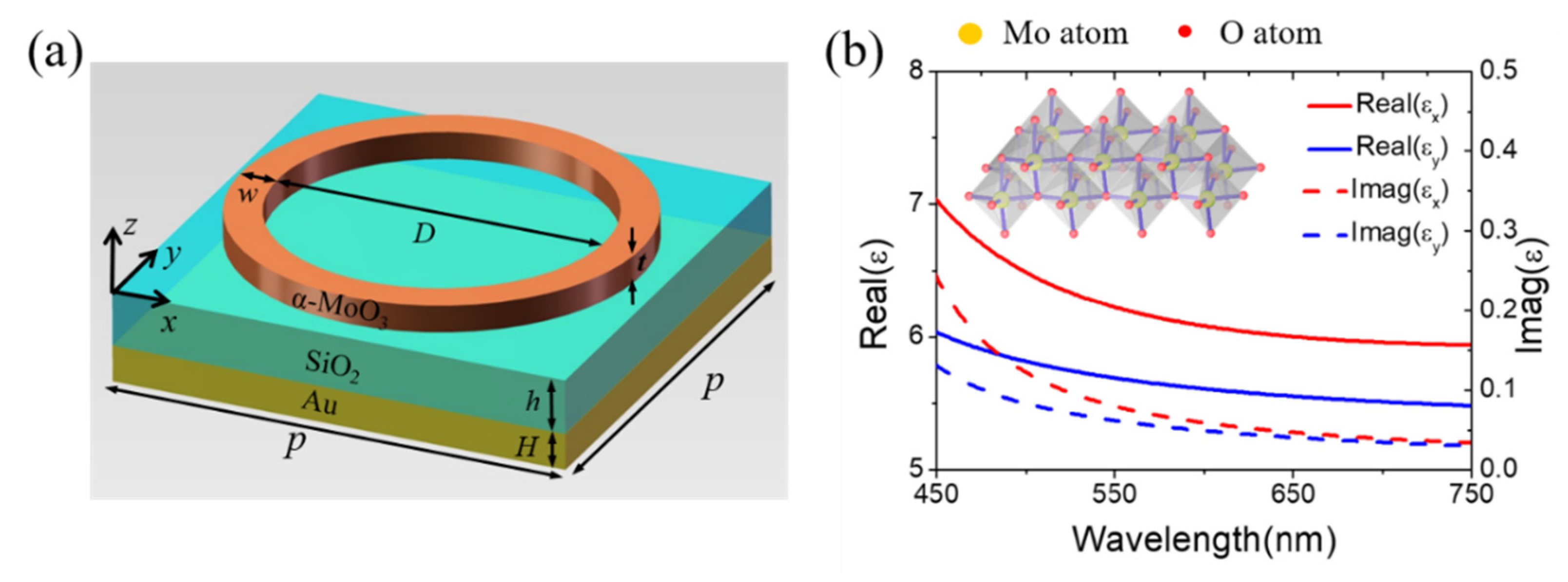
2. Structural Design and Simulation

Figure 1a shows schematically the unit cell of proposed anisotropic perfect absorber, which consists of top α-MoO3 ring and dielectric layer stacked on a gold mirror. The relevant geometric parameters and values are listed in the caption of Figure 1. As far as the process of fabrication, the multilayer structure can be fabricated by using physical vapor deposition techniques, which has been a well-known method for scalable and repeatable synthesis. In our design, the complex dielectric function of α-MoO3 can be described as follows [10]:
ε ( ω ) = ε + i ω pi 2 ω oi 2 + ω 2 - i γ i ω
where i indicates the number of Lorentz oscillators, ε, ωpi, ωoi, and γi refers to the high frequency dielectric constant, the plasma frequency, the eigenfrequency, and the scattering rate of the ith Lorentz oscillator, respectively. The parameters used in Equation (1) to calculate the permittivity tensors of α-MoO3 are listed in Table 1 [10].
Figure 1b illustrates the real and imaginary parts of α-MoO3 permittivity along [100] and [001] directions extracted from Ref. [10]. Full field electromagnetic calculations were performed by using Lumerical FDTD Solution software package. The three-dimensional FDTD simulations were made in a unit cell area, and the non-uniform mesh is chosen, and the mesh size gradually increases outside the α-MoO3 material. Following the crystallographic direction conventions, the x-, y-, and z-directions represent the [100], [001], and [010] directions, respectively. In calculations, the plane waves were illuminated along the negative z-direction, and periodic boundary conditions were used in x- and y-directions. In general, the optical absorption can be expressed as A = 1 − RT, where R and T indicate the reflection and transmission, respectively. Considering that the thickness of the gold mirror has exceeded the skin depth of the light, the transmission T is equal to zero. Therefore, the absorption coefficient A can be abbreviated as A = 1 − R. In addition, the dielectric layer is chosen to be SiO2 with a refractive index of 1.45, and the permittivity of gold is described by Drude model:
ε ( ω ) = ε ω p 2 ω 2 + i ω γ
where ω is the angular frequency, and the plasma frequency ωp is 1.37 × 10¹⁶ rad/s, the scattering rate γ = 4.08 × 10¹³ rad/s, and ε = 1.

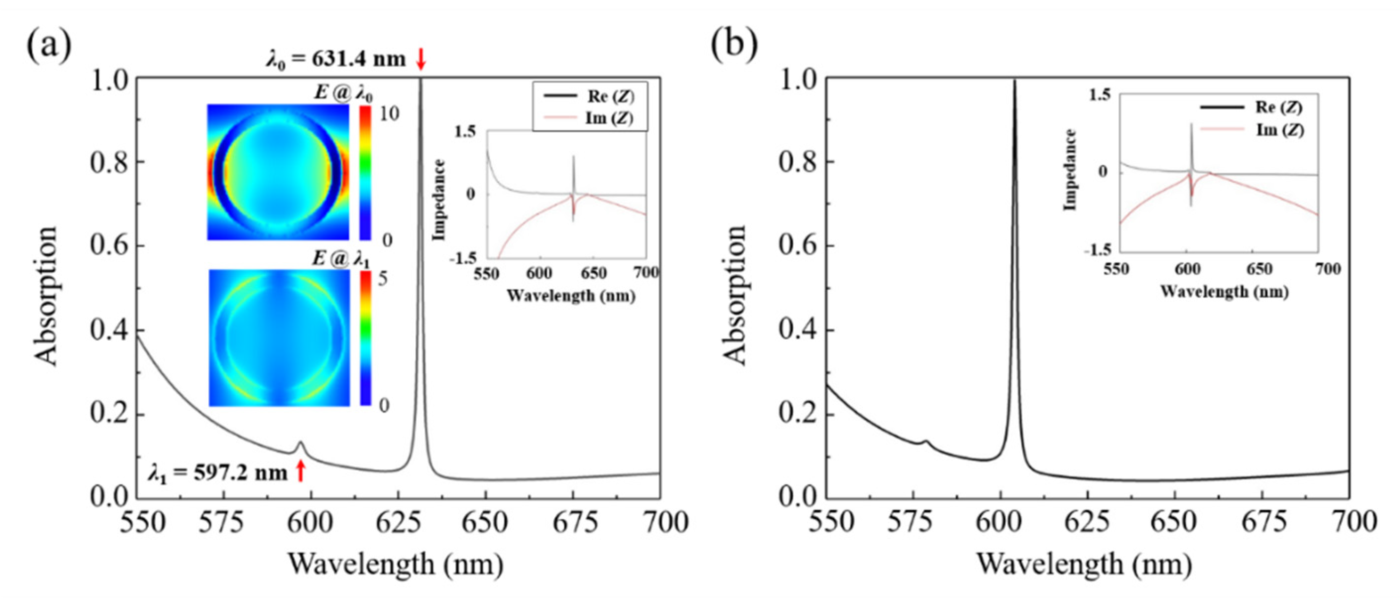
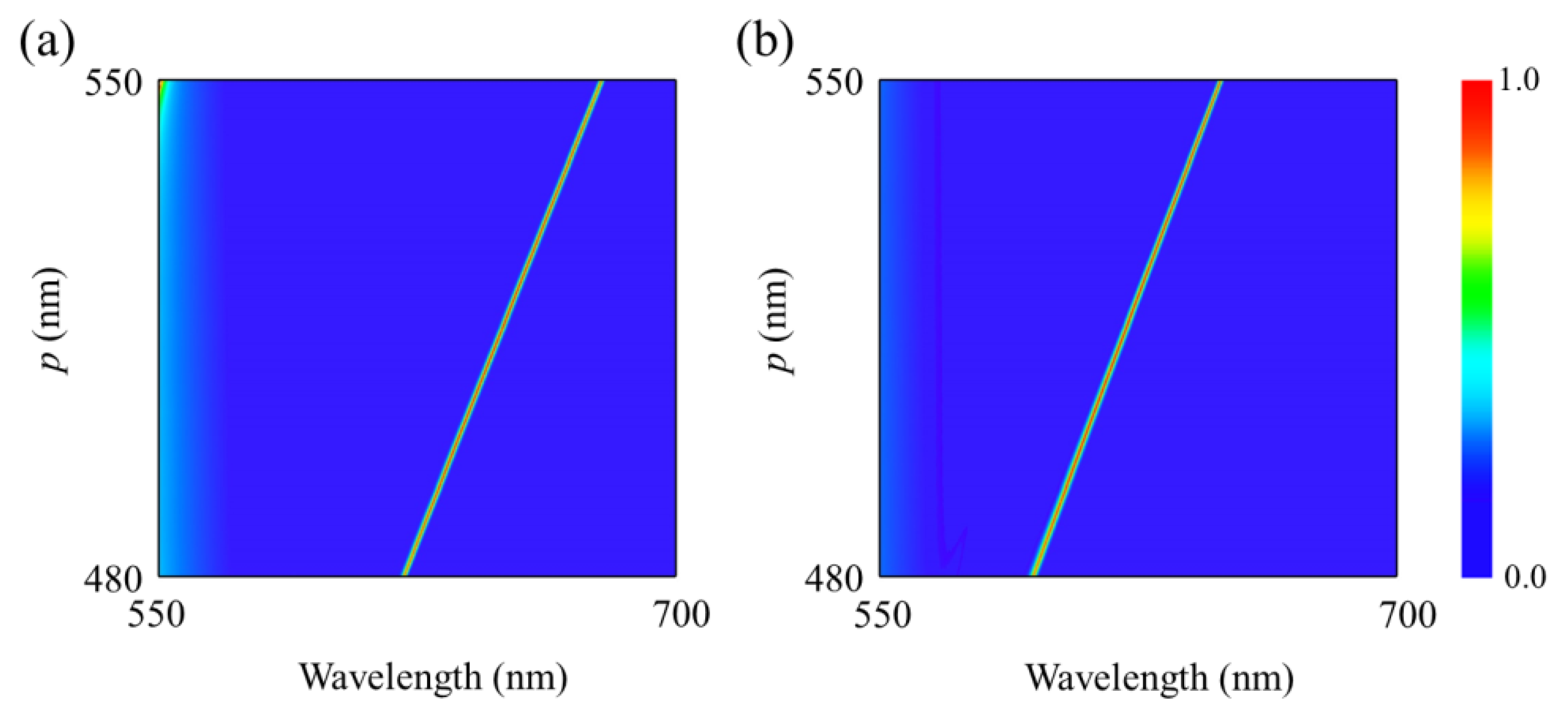
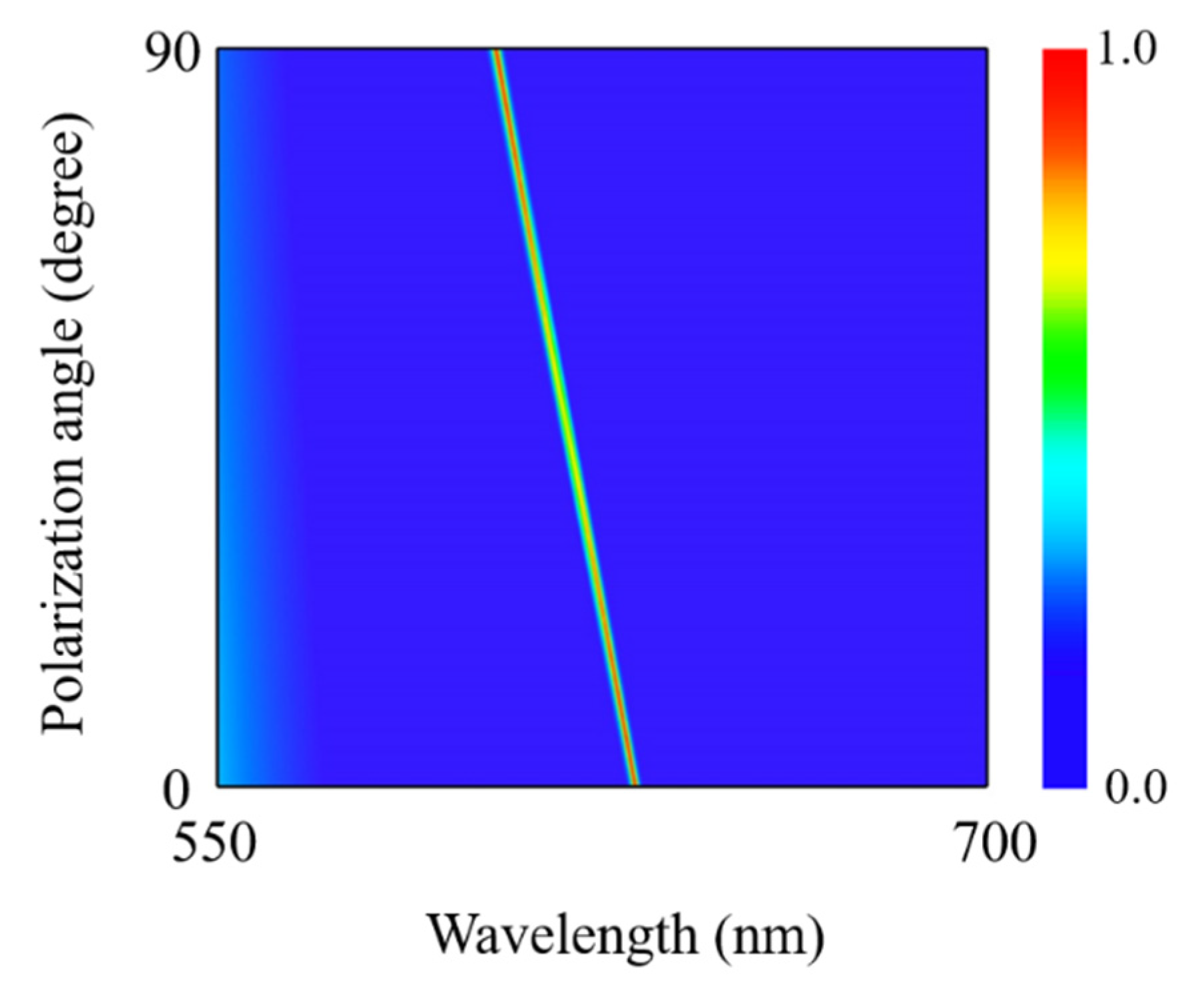
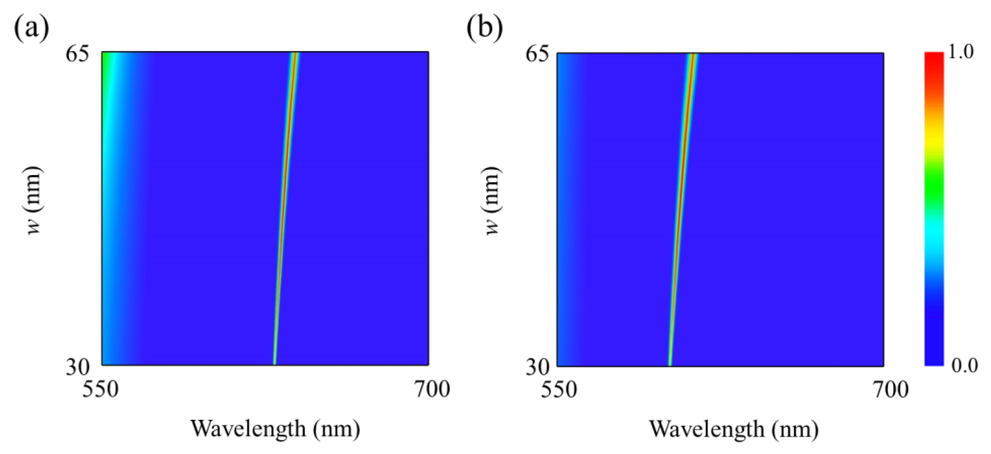
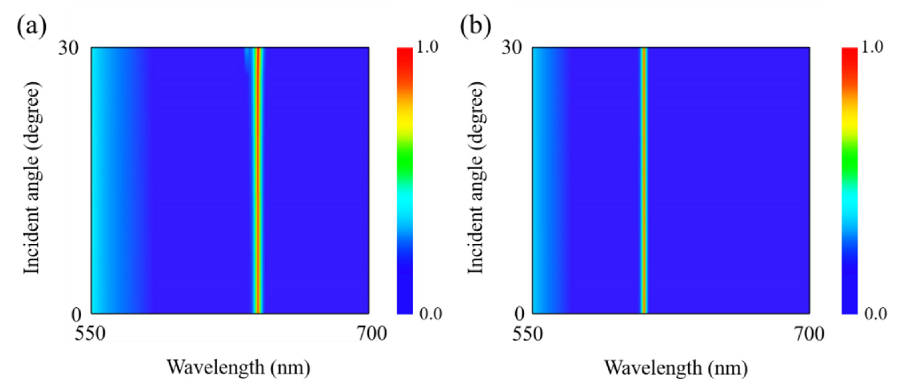
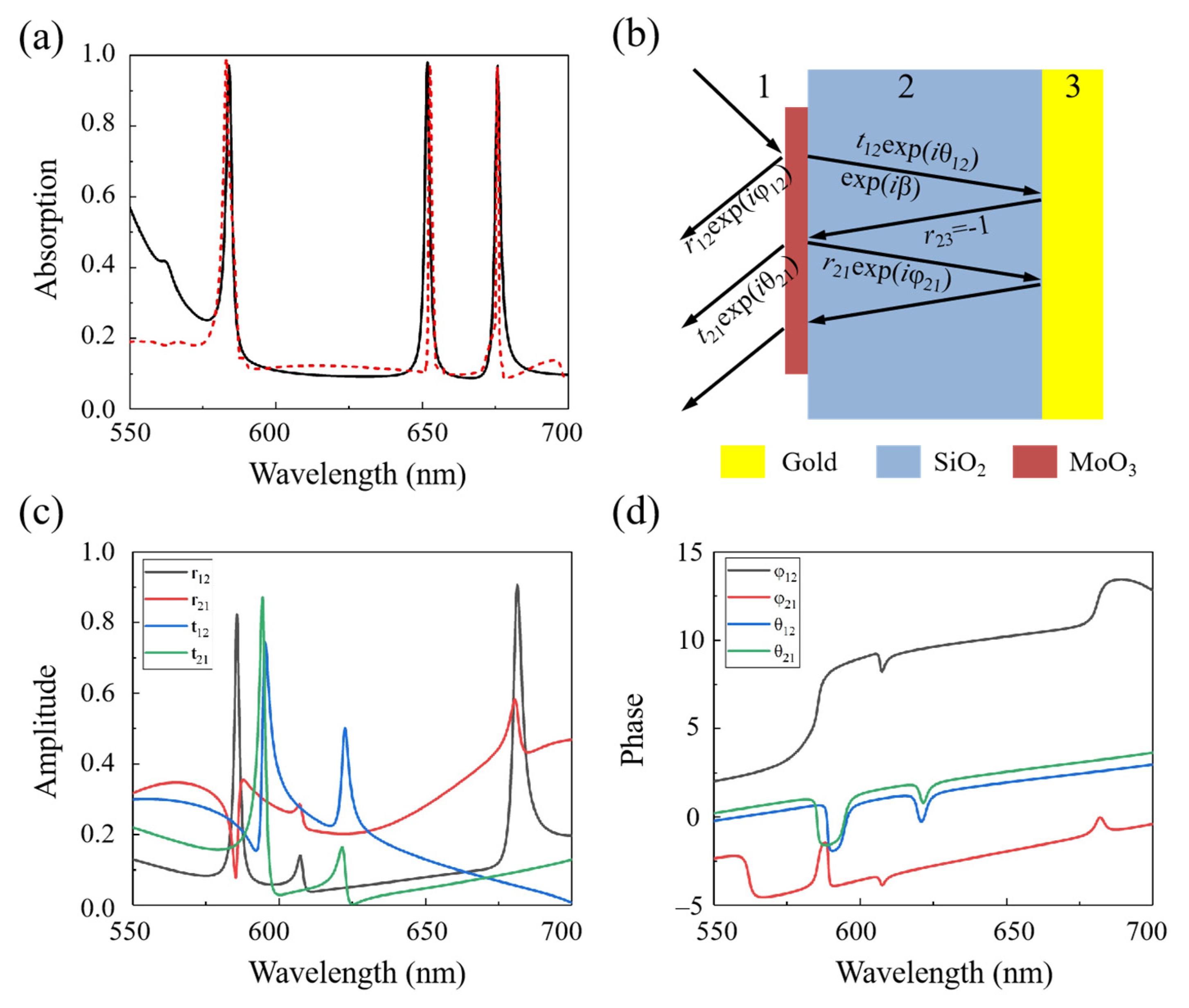
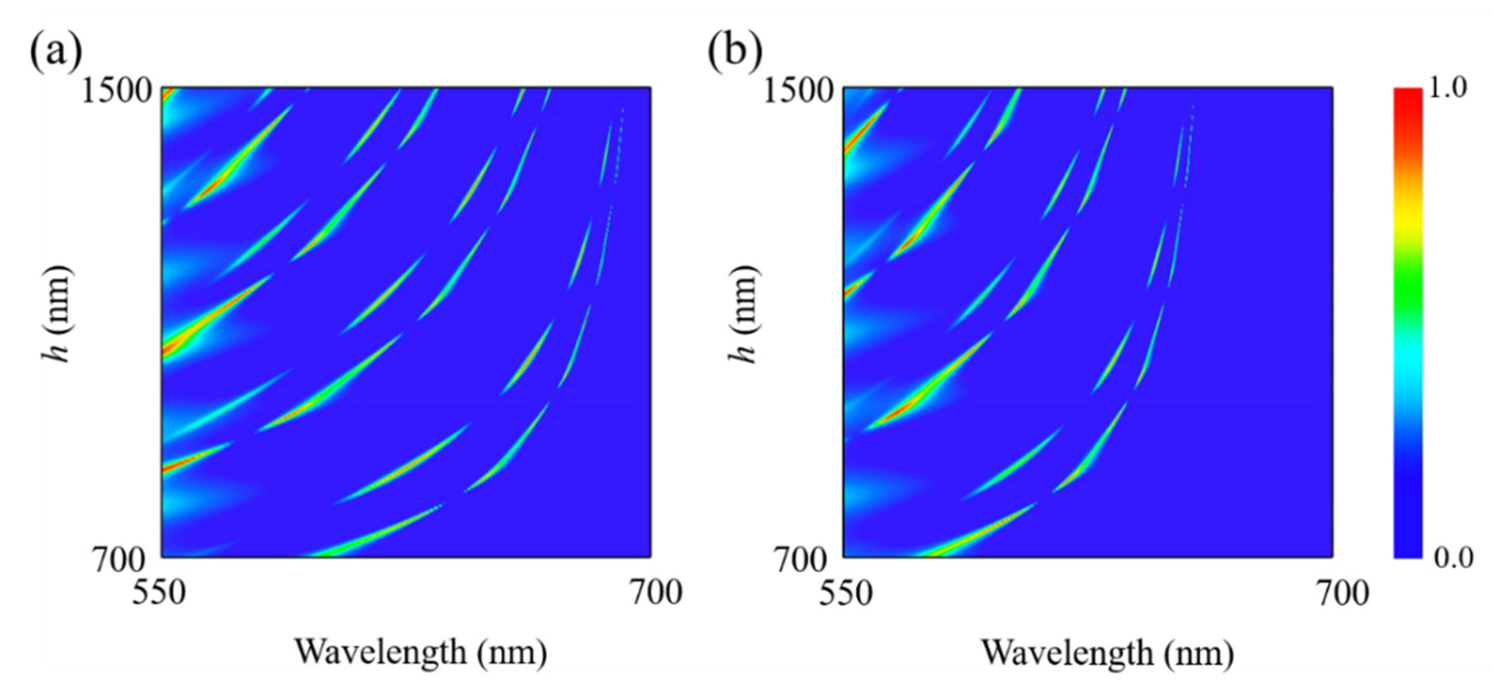
3. Results and Discussion

Figure 2 gives the optical absorption spectra of the designed metamaterial absorber when the polarization directions of incident lights are along the [100] and [001] crystal direction of α-MoO3, respectively. The simulation results show that the proposed absorber can achieve perfect absorption in both [100] and [001] crystal directions. It is shown from Figure 2a that the designed nanostructure can achieve an absorptivity of 99.72% at the wavelength of 631.4 nm when the polarization direction of light is along [100] crystal direction of α-MoO3. Meanwhile, there exists a weak absorption peak at 597.2 nm with absorptivity of 16.2%. In contrast, when the polarization direction of light is along [001] crystal direction of α-MoO3, the absorptivity reaches up to 99.28% at the resonant wavelength of 604.1 nm as shown in Figure 2b. The shift of resonance wavelength is attributable to the strong anisotropy of α-MoO3. Besides, according to the definition of quality factor Q, the total Q factor can be written by Q = f0f, in which f0 corresponds to the resonance frequency at the peak wavelength, and Δf represents the full width at half maximum. Thus, the calculated values of quality factors amount to 538.30 and 574.95 in the proposed α-MoO3–based metamaterial absorber for polarizations along [100] and [001] crystalline directions, respectively. In addition, the effective impedances of the absorber in the visible region are calculated as shown in the insets of Figure 2a,b. It is known that under critical coupling conditions, the effective impedance of structure system matches with that of free space (Z = Z0 = 1), which can be expressed as in which Z = ( 1 + S 11 ) 2   -   S 21 2 ( 1 S 21 ) 2   -   S 21 2 , where S11 and S21 denote as the scattering parameters relevant to reflectance and transmittance coefficient [45]. When the polarization directions are along the [100] and [001] crystal directions of α-MoO3, the corresponding effective impedances are Z1 = 0.92 − 0.12i and Z2 = 0.94 − 0.10i, respectively. It is demonstrated that the effective impedance of the absorber system matches well with the normalized impedance of the free space, which effectively suppresses the light reflection and achieves the perfect absorption. In order to manifest the underlying physical mechanism behind the resonant absorption phenomenon, the field distributions at the resonant wavelengths are given in the inset for polarization along [100] direction of α-MoO3. As shown in the insets, the electric field distribution at the resonance wavelength of 631.38 nm in x-y plane shows the characteristics of electric dipole, which is symmetric about the y-axis in viewing of the incidence polarization along [100] direction of α-MoO3. The localized collective electron excitations strongly couple with the incidence light, thus leading to the perfect electromagnetic waves absorption. Meanwhile, one can observe that there exists a weak resonance absorption peak at the wavelength of 597.2 nm, which is attributable to the excitation of electric quadrupole around the edge of α-MoO3 ring. Similarly, the operation mechanism also applies for the case of polarization along [001] crystal directions of α-MoO3.
To study the influences of geometric parameters on the optical absorption spectra, Figure 3 and Figure 4 calculate the optical absorption spectra as a function of wavelength and the width w of α-MoO3 nanoring as well as the period p of nanostructure. One can see from Figure 3 that when the width of α-MoO3 nanoring is increasing from 30 to 65 nm, the resonant wavelength of the absorptive spectra has a slight redshift for polarization along the [100] and [001] directions, respectively. Meanwhile, the absorption efficiency has an obvious enhancement with increasing of w. From Figure 4, it is clearly shown that the absorption spectra are closely related to the periodicity of nanostructure array. When the period p is increased from 480 to 550 nm, the resonant absorption peaks shift to the longer wavelength, and the different resonant wavelength for both polarizations originates from the strong anisotropy of lattice structure of α-MoO3 crystal. Therefore, one can modulate the optical absorption spectra by controlling the related geometric parameters.
To further explore the influences of polarization direction on the optical absorption spectra, Figure 5 calculates the optical absorption spectra as a function of wavelength and polarization angle. One can see from Figure 5 that when the polarization angle is gradually increased from 0° (x-polarization) to 90° (y-polarization), the optical spectrum displays an ultra-narrowband resonant absorption peak, which has also a blue-shift from 631.4 nm to 604.1 nm due to the anisotropic lattice structure of α-MoO3. Meanwhile, the absorptivity at the resonant wavelength also changes with increasing of the polarization angle. Especially, the optical absorptivity reaches up to perfect absorption when the polarization angle takes the value of 0° or 90°. Therefore, the optical absorption spectra exhibit a polarization-dependent characteristic even though the geometric structure is circularly symmetric. Furthermore, the absorption performance of the absorber under oblique incidence is also investigated. Figure 6 calculates the optical absorption spectra as a function of wavelength and incident angle. It can be clearly seen from Figure 6 that when the incident angle is increased from 0° to 30°, the optical spectra take on an ultra-narrowband perfect absorption for both polarizations along [100] and [001] directions of α-MoO3, respectively. The absorption performance in both [100] and [001] directions is insensitive to the incident angle. Meanwhile, the positions of resonant absorption peaks almost keep invariant for both polarization directions. Comparing Figure 6a,b, the resonant wavelength has a blue shift when the polarization is switched from [100] direction to [001] direction of α-MoO3.
The above mentioned single-band perfect absorption can be extended to multi-band absorption as shown in Figure 7a. It can be seen from Figure 7a that there are three nearly perfect absorption bands when the dielectric spacer takes the value of 500 nm as shown by the black line. The phenomenon of triple-band absorption can be explained by interference theory in Fabry–Pérot cavity. As shown in the Figure 7b, the incident light is partially reflected back to air with a reflection coefficient r ~ 12 = r12e12 and partially transmitted into the dielectric layer with a transmission coefficient t ~ 12 = t12eiθ12 at the air-spacer interface with α-MoO3 ring. In the model of interference theory, the lights are reflected back and forth between the α-MoO3 ring and metal substrate, with a complex propagation phase β = ε ~ k 0 h , where ε ~ is the permittivity of the dielectric spacer, k0 is the wavenumber of free space, and h is the thickness of the dielectric spacer. Plus, there appear partial reflection with coefficients r ~ 21 = r21e21 and transmission with coefficients t ~ 21 = t21eiθ21 at the air-spacer interface with α-MoO3 ring. The total reflection is the superposition of the multiple reflection [46]:
r ~ = r ~ 12 t ~ 12 t ~ 21 e i 2 β 1 + r ~ 21 e i 2 β
The absorbance can be calculated through A ~ (ω) = 1 − | r ~ (ω)|2, where r ~ (ω) is the total reflection originating from the superposition of multiple reflection. Take the h = 500 nm of the proposed absorber as an example, as shown in the Figure 7a, the results of interference theory (red dashed line) are consistent well with the numerical simulations (black line). The amplitude and phase corresponding to t ~ 12, t ~ 21, r ~ 12, and r ~ 21 are shown in Figure 7c,d, respectively. Therefore, one can conclude that the proposed absorber can obtain arbitrary number of absorption bands in the visible light region by choosing appropriate thickness of the dielectric layer.
To demonstrate the effect of dielectric layer thickness h on the resonant absorption of the structure, Figure 8 gives the absorption spectra of the proposed nanostructure as a function of wavelength and the dielectric layer thickness. It can be clearly seen from Figure 8 that for polarizations along the [100] and [001] crystal directions of α-MoO3, the resonance absorption of the absorber can be adjusted from one peak to multiple peaks by choosing suitable dielectric layer thickness, i.e., h = 1500 nm. Similar to the triple-band absorption phenomena, the multi-band absorption can also be interpreted by interference theory in Fabry–Pérot cavity. Plus, one can conclude from the model of interference theory that the dielectric thickness plays an important role in determining the resonance wavelength of Fabry–Pérot cavity. As a result, with increasing of the dielectric layer thickness, all the resonance peaks exhibit the tendency of redshift. The maximum optical absorbance appears at the constructive interference with approximate phase match condition of 2 β + φ + π 2 m π , where φ means the phase shift, and m is an integer.

4. Conclusions

In conclusion, we theoretically proposed and numerically demonstrated an ultra-narrowband anisotropic metamaterial perfect absorber based on α-MoO3, unit cell of which consists of an α-MoO3 ring and dielectric layer stacked on a gold mirror. The numerical results show that the ultra-narrowband perfect absorption can be obtained in the visible light band for polarizations along the [100] and [001] crystal directions of α-MoO3. Plus, the influences of some geometric parameters on the optical absorption spectra are discussed. Meanwhile, the proposed anisotropic metamaterial absorber has an excellent angular tolerance for the case of oblique incidence. Especially, the single-band perfect absorption in our proposed metamaterials can be arbitrarily developed into multi-band perfect absorption by choosing the suitable thickness of dielectric layer. The physical mechanism can be explained by the interference theory in Fabry–Pérot cavity, which is consistent with the numerical simulation. Our research results have some potential applications in designs of anisotropic meta-devices with tunable spectra and selective polarization in the visible light region.

Author Contributions

Conceptualization, G.J. and B.T.; methodology, G.J. and T.Z.; software, G.J.; validation, G.J., T.Z. and B.T.; formal analysis, B.T.; investigation, B.T.; resources, G.J.; data curation, G.J.; writing—original draft preparation, B.T.; writing—review and editing, B.T.; visualization, G.J. and B.T.; supervision, B.T.; project administration, B.T.; funding acquisition, B.T. and G.J. All authors have read and agreed to the published version of the manuscript.

Funding

This research was supported by the applied Characteristic Disciplines of Electronic Science and Technology of Xiangnan University, and Natural Science Foundation of Jiangsu Province (BK20201446).

Institutional Review Board Statement

Not applicable.

Informed Consent Statement

Not applicable.

Data Availability Statement

The data are included in the main text.

Conflicts of Interest

The authors declare no conflict of interest.

References

  1. Zhu, Y.; Murali, S.; Cai, W.; Li, X.; Suk, J.W.; Potts, J.R.; Ruoff, R.S. Graphene and graphene oxide: Synthesis, properties, and applications. Adv. Mater. 2010, 22, 3906–3924. [Google Scholar] [CrossRef] [PubMed]
  2. Liu, Z.; Aydin, K. Localized Surface Plasmons in Nanostructured Monolayer Black Phosphorus. Nano lett. 2016, 16, 3457–3462. [Google Scholar] [CrossRef] [PubMed]
  3. Song, L.; Ci, L.; Lu, H.; Sorokin, P.B.; Jin, C.; Ni, J.; Kvashnin, A.G.; Kvashnin, D.G.; Lou, J.; Yakobson, B.I.; et al. Large scale growth and characterization of atomic hexagonal boron nitride layers. Nano lett. 2010, 10, 3209–3215. [Google Scholar] [CrossRef] [PubMed]
  4. Wang, Q.H.; Kalantar-Zadeh, K.; Kis, A.; Coleman, J.N.; Strano, M.S. Electronics and optoelectronics of two-dimensional transition metal dichalcogenides. Nat. Nanotechnol. 2012, 7, 699–712. [Google Scholar] [CrossRef] [PubMed]
  5. Jia, Z.; Huang, L.; Su, J.; Tang, B. Tunable plasmon-induced transparency based on monolayer black phosphorus by bright-dark mode coupling. Appl. Phy. Express 2020, 13, 072006. [Google Scholar] [CrossRef]
  6. Ma, W.; Alonso-Gonzalez, P.; Li, S.; Nikitin, A.Y.; Yuan, J.; Martin-Sanchez, J.; Taboada-Gutierrez, J.; Amenabar, I.; Li, P.; Velez, S.; et al. In-plane anisotropic and ultra-low-loss polaritons in a natural van der Waals crystal. Nature 2018, 562, 557–562. [Google Scholar] [CrossRef] [Green Version]
  7. Zheng, Z.; Xu, N.; Oscurato, S.L.; Tamagnone, M.; Sun, F.; Jiang, Y.; Ke, Y.; Chen, J.; Huang, W.; Wilson, W.L. A mid-infrared biaxial hyperbolic van der Waals crystal. Sci. Adv. 2019, 5, eaav8690. [Google Scholar] [CrossRef] [Green Version]
  8. Zhu, H.; Xu, Z.; Cai, L.; Wang, H.; Luo, H.; Pattanayak, A.; Ghosh, P.; Qiu, M.; Li, Q. Ultrathin High Quality-Factor Planar Absorbers/Emitters Based on Uniaxial/Biaxial Anisotropic van der Waals Polar Crystals. Adv. Opt. Mater. 2021, 9, 2100645. [Google Scholar] [CrossRef]
  9. Álvarez-Pérez, G.; Folland, T.G.; Errea, I.; Taboada-Gutiérrez, J.; Duan, J.; Martín-Sánchez, J.; Tresguerres-Mata, A.I.; Matson, J.R.; Bylinkin, A.; He, M. Infrared permittivity of the biaxial van der waals semiconductor α-MoO3 from near-and far-field correlative studies. Adv. Mater. 2020, 32, 1908176. [Google Scholar] [CrossRef]
  10. Wei, C.; Abedini Dereshgi, S.; Song, X.; Murthy, A.; Dravid, V.P.; Cao, T.; Aydin, K. Polarization Reflector/Color Filter at Visible Frequencies via Anisotropic α-MoO3. Adv. Opt. Mater. 2020, 8, 2000088. [Google Scholar] [CrossRef]
  11. Abedini Dereshgi, S.; Folland, T.G.; Murthy, A.A.; Song, X.; Tanriover, I.; Dravid, V.P.; Caldwell, J.D.; Aydin, K. Lithography-free IR polarization converters via orthogonal in-plane phonons in alpha-MoO3 flakes. Nat. Commun. 2020, 11, 5771. [Google Scholar] [CrossRef] [PubMed]
  12. Dai, Z.; Hu, G.; Si, G.; Ou, Q.; Zhang, Q.; Balendhran, S.; Rahman, F.; Zhang, B.Y.; Ou, J.Z.; Li, G. Edge-oriented and steerable hyperbolic polaritons in anisotropic van der Waals nanocavities. Nat. Commun. 2020, 11, 6086. [Google Scholar] [CrossRef]
  13. Qu, Y.; Chen, N.; Teng, H.; Hu, H.; Sun, J.; Yu, R.; Hu, D.; Xue, M.; Li, C.; Wu, B. Tunable planar focusing based on hyperbolic phonon polaritons in α-MoO3. Adv. Mater. 2022, 2105590. [Google Scholar] [CrossRef] [PubMed]
  14. Hu, G.; Ou, Q.; Si, G.; Wu, Y.; Wu, J.; Dai, Z.; Krasnok, A.; Mazor, Y.; Zhang, Q.; Bao, Q. Topological polaritons and photonic magic angles in twisted α-MoO3 bilayers. Nature 2020, 582, 209–213. [Google Scholar] [CrossRef] [PubMed]
  15. Smith, D.R.; Padilla, W.J.; Vier, D.; Nemat-Nasser, S.C.; Schultz, S. Composite medium with simultaneously negative permeability and permittivity. Phys. Rev. Lett. 2000, 84, 4184. [Google Scholar] [CrossRef] [PubMed] [Green Version]
  16. Xiao, S.; Wang, T.; Liu, T.; Zhou, C.; Jiang, X.; Zhang, J. Active metamaterials and metadevices: A review. J. Phys. D Appl. Phys. 2020, 53, 503002. [Google Scholar] [CrossRef]
  17. Ren, Y.; Tang, B. Switchable Multi-Functional VO2-Integrated Metamaterial Devices in the Terahertz Region. J. Lightwave Technol. 2021, 39, 5864–5868. [Google Scholar] [CrossRef]
  18. Ren, Y.; Zhou, T.; Jiang, C.; Tang, B. Thermally switching between perfect absorber and asymmetric transmission in vanadium dioxide-assisted metamaterials. Opt. Express 2021, 29, 7666–7679. [Google Scholar] [CrossRef]
  19. Landy, N.I.; Sajuyigbe, S.; Mock, J.J.; Smith, D.R.; Padilla, W.J. Perfect metamaterial absorber. Phys. Rev. Lett. 2008, 100, 207402. [Google Scholar] [CrossRef]
  20. Li, Z.; Butun, S.; Aydin, K. Ultranarrow band absorbers based on surface lattice resonances in nanostructured metal surfaces. ACS Nano 2014, 8, 8242–8248. [Google Scholar] [CrossRef]
  21. Tang, B.; Li, Z.; Palacios, E.; Liu, Z.; Butun, S.; Aydin, K. Chiral-selective plasmonic metasurface absorbers operating at visible frequencies. IEEE Photonics Technol. Lett. 2017, 29, 295–298. [Google Scholar] [CrossRef]
  22. Li, Z.; Palacios, E.; Butun, S.; Kocer, H.; Aydin, K. Omnidirectional, broadband light absorption using large-area, ultrathin lossy metallic film coatings. Sci. Rep. 2015, 5, 15137. [Google Scholar] [CrossRef] [PubMed]
  23. Tang, B.; Zhu, Y.; Zhou, X.; Huang, L.; Lang, X. Wide-Angle Polarization-Independent Broadband Absorbers Based on Concentric Multisplit Ring Arrays. IEEE Photonics J. 2017, 9, 1–7. [Google Scholar] [CrossRef]
  24. Li, Z.; Yi, Y.; Xu, D.; Yang, H.; Yi, Z.; Chen, X.; Yi, Y.; Zhang, J.; Wu, P. A multi-band and polarization-independent perfect absorber based on Dirac semimetals circles and semi-ellipses array. Chin. Phys. B 2021, 30, 098102. [Google Scholar] [CrossRef]
  25. Chen, Z.; Chen, H.; Jile, H.; Xu, D.; Yi, Z.; Lei, Y.; Chen, X.; Zhou, Z.; Cai, S.; Li, G. Multi-band multi-tunable perfect plasmon absorber based on L-shaped and double-elliptical graphene stacks. Diam. Relat. Mater. 2021, 115, 108374. [Google Scholar] [CrossRef]
  26. Zhou, F.; Qin, F.; Yi, Z.; Yao, W.; Liu, Z.; Wu, X.; Wu, P. Ultra-wideband and wide-angle perfect solar energy absorber based on Ti nanorings surface plasmon resonance. Phys. Chem. Chem. Phys. 2021, 23, 17041–17048. [Google Scholar] [CrossRef] [PubMed]
  27. Liu, N.; Mesch, M.; Weiss, T.; Hentschel, M.; Giessen, H. Infrared perfect absorber and its application as plasmonic sensor. Nano Lett. 2010, 10, 2342–2348. [Google Scholar] [CrossRef]
  28. Kravets, V.G.; Schedin, F.; Jalil, R.; Britnell, L.; Gorbachev, R.V.; Ansell, D.; Thackray, B.; Novoselov, K.S.; Geim, A.K.; Kabashin, A.V.; et al. Singular phase nano-optics in plasmonic metamaterials for label-free single-molecule detection. Nat. Mater. 2013, 12, 304–309. [Google Scholar] [CrossRef]
  29. Xu, Z.; Li, Q.; Du, K.; Long, S.; Yang, Y.; Cao, X.; Luo, H.; Zhu, H.; Ghosh, P.; Shen, W. Spatially resolved dynamically reconfigurable multilevel control of thermal emission. Laser Photonics Rev. 2020, 14, 1900162. [Google Scholar] [CrossRef]
  30. Xiong, F.; Zhang, J.; Zhu, Z.; Yuan, X.; Qin, S. Strong anisotropic perfect absorption in monolayer black phosphorous and its application as tunable polarizer. J. Opt. 2017, 19, 075002. [Google Scholar] [CrossRef]
  31. Tang, B.; Yang, N.; Huang, L.; Su, J.; Jiang, C. Tunable Anisotropic Perfect Enhancement Absorption in Black Phosphorus-Based Metasurfaces. IEEE Photonics J. 2020, 12, 1–9. [Google Scholar] [CrossRef]
  32. Audhkhasi, R.; Povinelli, M.L. Gold-black phosphorus nanostructured absorbers for efficient light trapping in the mid-infrared. Opt. Express 2020, 28, 19562–19570. [Google Scholar] [CrossRef] [PubMed]
  33. Liu, Z.; Zhou, J.; Liu, X.; Fu, G.; Liu, G.; Tang, C.; Chen, J. High-Q plasmonic graphene absorbers for electrical switching and optical detection. Carbon 2020, 166, 256–264. [Google Scholar] [CrossRef]
  34. Liu, T.; Zhou, C.; Xiao, S. Gain-assisted critical coupling for enhanced optical absorption in graphene. Nanotechnology 2021, 32, 205202. [Google Scholar] [CrossRef]
  35. Xiao, S.; Liu, T.; Wang, X.; Liu, X.; Zhou, C. Tailoring the absorption bandwidth of graphene at critical coupling. Phy. Rev. B 2020, 102, 085410. [Google Scholar] [CrossRef]
  36. Sang, T.; Dereshgi, S.A.; Hadibrata, W.; Tanriover, I.; Aydin, K. Highly efficient light absorption of monolayer graphene by quasi-bound state in the continuum. Nanomaterials 2021, 11, 484. [Google Scholar] [CrossRef]
  37. Li, J.; Chen, Z.; Yang, H.; Yi, Z.; Chen, X.; Yao, W.; Duan, T.; Wu, P.; Li, G.; Yi, Y. Tunable Broadband Solar Energy Absorber Based on Monolayer Transition Metal Dichalcogenides Materials Using Au Nanocubes. Nanomaterials 2020, 10, 257. [Google Scholar] [CrossRef] [Green Version]
  38. Thongrattanasiri, S.; Koppens, F.H.; De Abajo, F.J.G. Complete optical absorption in periodically patterned graphene. Phys. Rev. Lett. 2012, 108, 047401. [Google Scholar] [CrossRef] [Green Version]
  39. Qi, H.; Sang, T.; Yin, X.; Wang, X.; Li, G. Dual-band absorption enhancement of monolayer molybdenum disulfide by a tapered metamaterial waveguide slab. Appl. Phys. Express 2020, 13, 065001. [Google Scholar] [CrossRef]
  40. Zhu, Y.; Tang, B.; Jiang, C. Tunable ultra-broadband anisotropic absorbers based on multi-layer black phosphorus ribbons. Appl. Phy. Express 2019, 12, 032009. [Google Scholar] [CrossRef]
  41. Zhu, Y.; Tang, B.; Yang, N.; Lang, X.; Su, J.; Li, Z. Tunable wide-angle perfect absorber based on black phosphorous-dielectric-metallic hybrid architecture. Phys. E Low-Dimens. Syst. Nanostruct. 2021, 126, 114449. [Google Scholar] [CrossRef]
  42. Deng, G.; Dereshgi, S.A.; Song, X.; Wei, C.; Aydin, K. Phonon-polariton assisted broadband resonant absorption in anisotropic α-phase MoO3 nanostructures. Phy. Rev. B 2020, 102, 035408. [Google Scholar] [CrossRef]
  43. Tang, B.; Yang, N.; Song, X.; Jin, G.; Su, J. Triple-Band Anisotropic Perfect Absorbers Based on α-Phase MoO3 Metamaterials in Visible Frequencies. Nanomaterials 2021, 11, 2061. [Google Scholar] [CrossRef] [PubMed]
  44. Dong, D.; Liu, Y.; Fu, Y. Critical Coupling and Perfect Absorption Using α-MoO3 Multilayers in the Mid-Infrared. Ann. Der Phys. 2021, 533, 2000512. [Google Scholar] [CrossRef]
  45. Smith, D.R.; Vier, D.C.; Koschny, T.; Soukoulis, C.M. Electromagnetic parameter retrieval from inhomogeneous metamaterials. Phys. Review. E Stat. Nonlinear Soft Matter Phys. 2005, 71, 036617. [Google Scholar] [CrossRef] [Green Version]
  46. Chen, H.-T. Interference theory of metamaterial perfect absorbers. Opt. Express 2012, 20, 7165–7172. [Google Scholar] [CrossRef] [Green Version]
Figure 1. (a) The structure unit cell diagram of the proposed absorber consisting of top α-MoO3 ring and SiO2 layer stacked on a gold substrate. In this design, the geometrical parameters are listed as follows: H = 200 nm, h = 300 nm, w = 40 nm, D = 360 nm, p = 500 nm, and the thickness of α-MoO3 ring t = 105 nm. (b) The real part and imaginary part of the α-MoO3 permittivity in the visible region. The inset is the schematic of the α-MoO3 material with layered structure. The yellow and red spheres represent molybdenum and oxygen atoms, respectively.
Nanomaterials 12 01375 g001
Figure 2. (a) Simulated absorption spectra for the proposed α-MoO3 absorber structure along the [100] directions. (b) Simulated absorption spectra for the proposed α-MoO3 absorber structure along the [001] directions. The subgraphs of Figure 2 represent the calculated real and imaginary parts of the effective impedance along the [100] and [001] directions, respectively.
Nanomaterials 12 01375 g002
Figure 3. Absorption spectra of the proposed structure as a function of wavelength and width w of nanoring for polarizations along (a) [100] and (b) [001] crystalline directions of α-MoO3. h = 300 nm, p = 500 nm, and t = 105 nm.
Nanomaterials 12 01375 g003
Figure 4. Absorption spectra of the proposed structure as a function of wavelength and period p for polarizations along (a) [100] and (b) [001] crystalline directions of α-MoO3. h = 300 nm, w = 40 nm, and t = 105 nm.
Nanomaterials 12 01375 g004
Figure 5. Absorption spectra of the proposed structure as a function of wavelength and polarization angle of incident light. P = 500 nm, w = 40 nm, t = 105 nm, and h = 300 nm.
Nanomaterials 12 01375 g005
Figure 6. Absorption spectra of the proposed structure as a function of wavelength and the incident angle with polarization along (a) [100] and (b) [001] crystalline directions of α-MoO3. p = 500 nm, w = 40 nm, t = 105 nm, and h = 300 nm.
Nanomaterials 12 01375 g006
Figure 7. (a) The simulated absorption spectrum (black curve) of the absorber with a thickness of h = 500 nm and the calculated absorption spectrum based on the interference theory (red curve). (b) The interference theory model of the propose absorber. (c) Amplitude and (d) phase of the reflection and transmission coefficients obtained from proposed absorber, respectively.
Nanomaterials 12 01375 g007
Figure 8. Absorption spectra of the proposed structure as a function of wavelength and the thickness of dielectric layer h for incident polarization along (a) [100] and (b) [001] crystalline directions of α-MoO3. p = 500 nm, w = 40 nm, and t = 105 nm.
Nanomaterials 12 01375 g008
Table 1. Parameters used in Equation (1) to obtain the permittivity tensors of α-MoO3 in the visible range.
Polarizationεωpj [cm−1]ω0 [cm−1]γj [cm−1]
x5.06521,67227,0191342.2
y4.50229,07832,2712027.1
Publisher’s Note: MDPI stays neutral with regard to jurisdictional claims in published maps and institutional affiliations.

