MoSe2-WS2 Nanostructure for an Efficient Hydrogen Generation under White Light LED Irradiation

 , , and
Abstract
:1. Introduction
2. Materials and Methods
2.1. Preparation of WS2
2.2. Preparation of MoSe2-WS2
2.3. Instruments
2.4. Photocatalytic Hydrogen Tests
2.5. Electrochemical Measurements
3. Results and Discussion
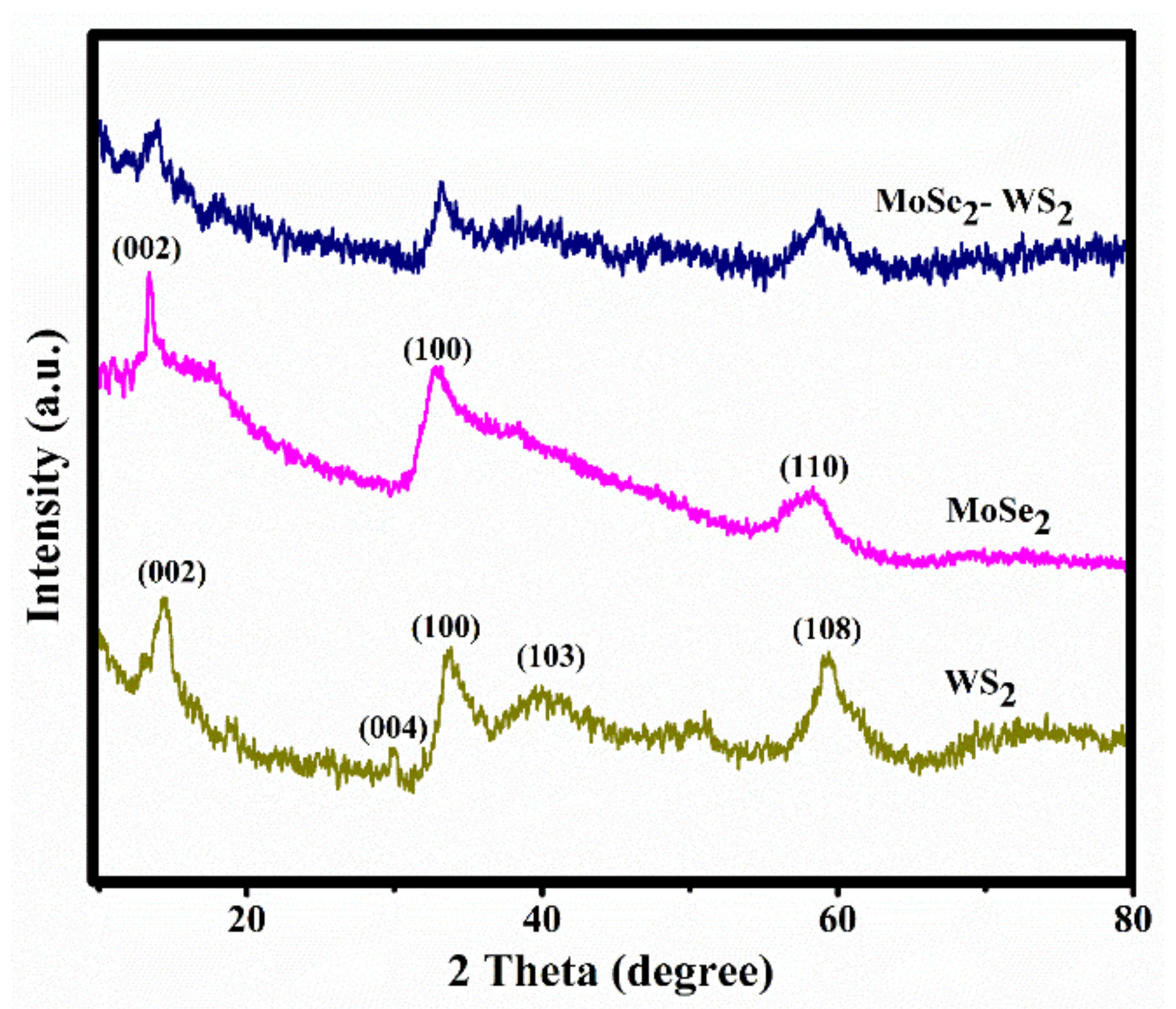
3.1. XRD Analysis
3.2. Morphology and Elemental Analysis
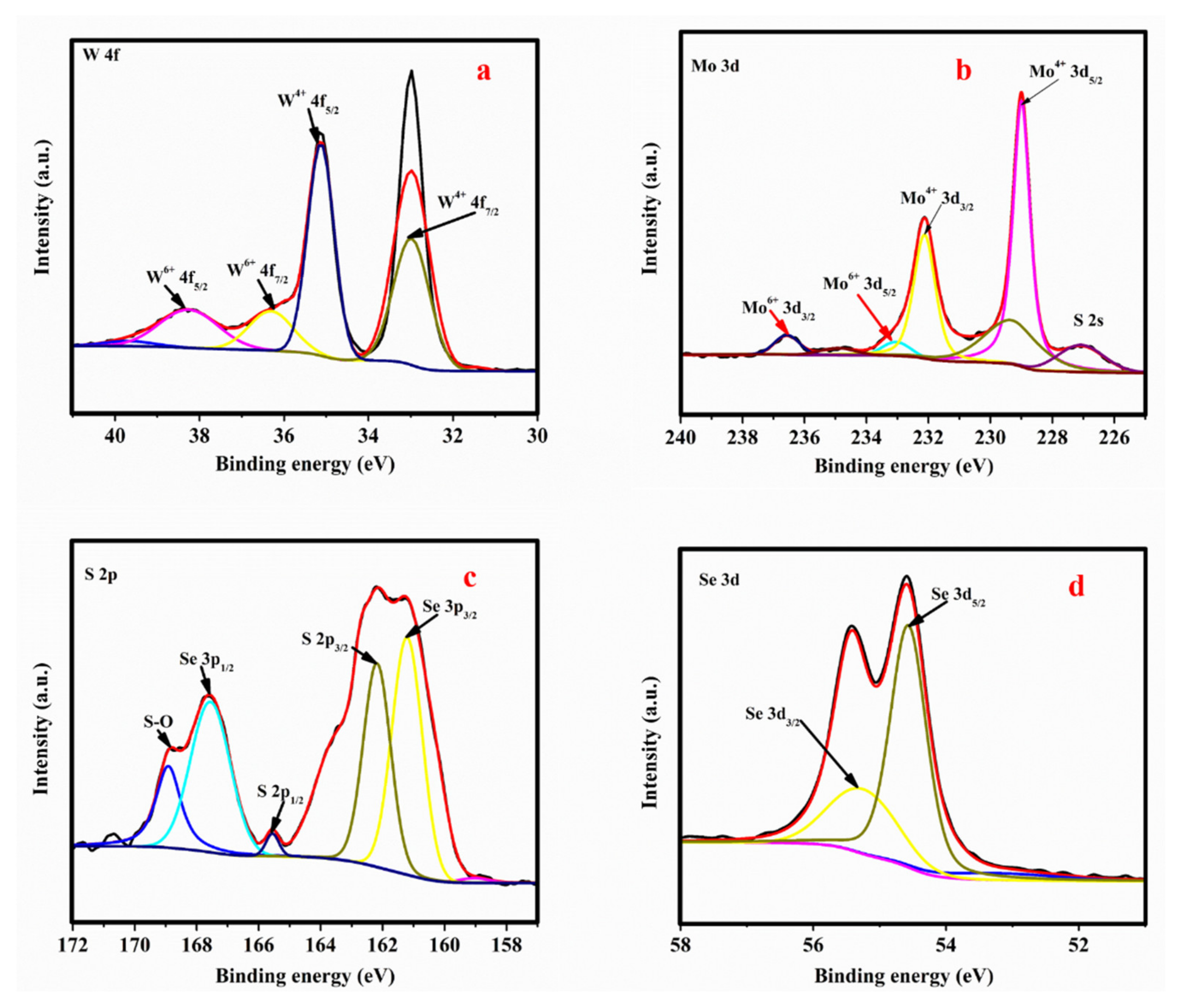
3.3. XPS Analysis
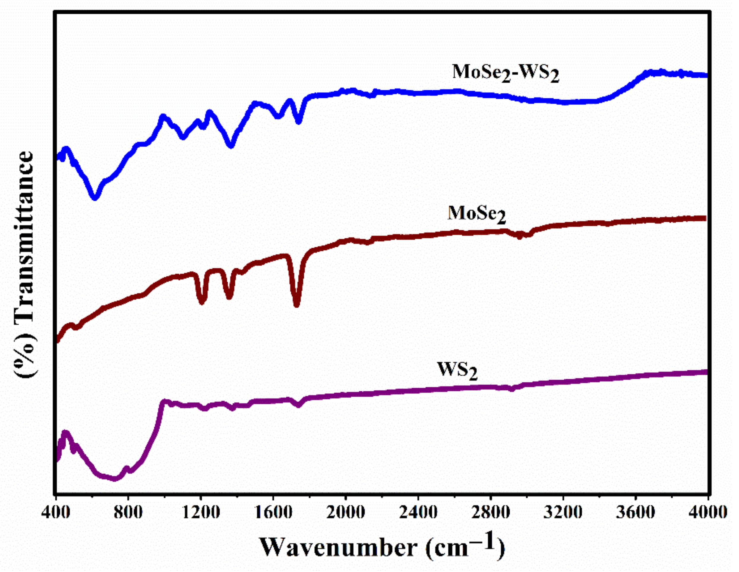
3.4. FTIR Analysis
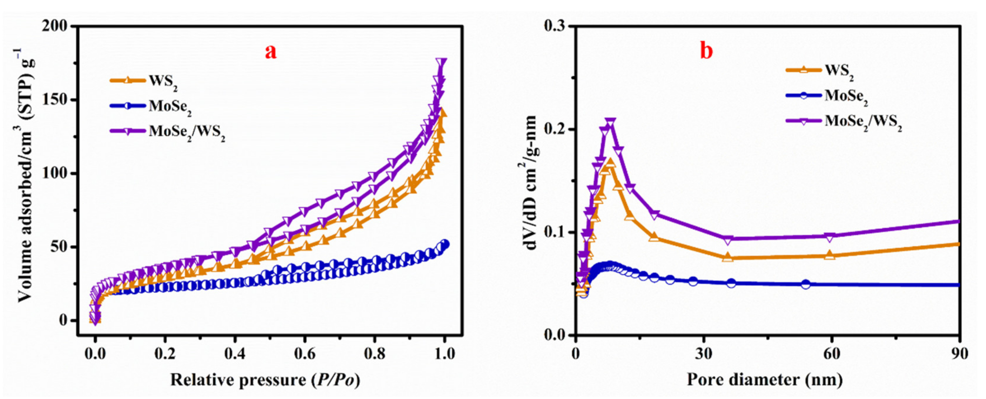
3.5. Surface Area Analysis
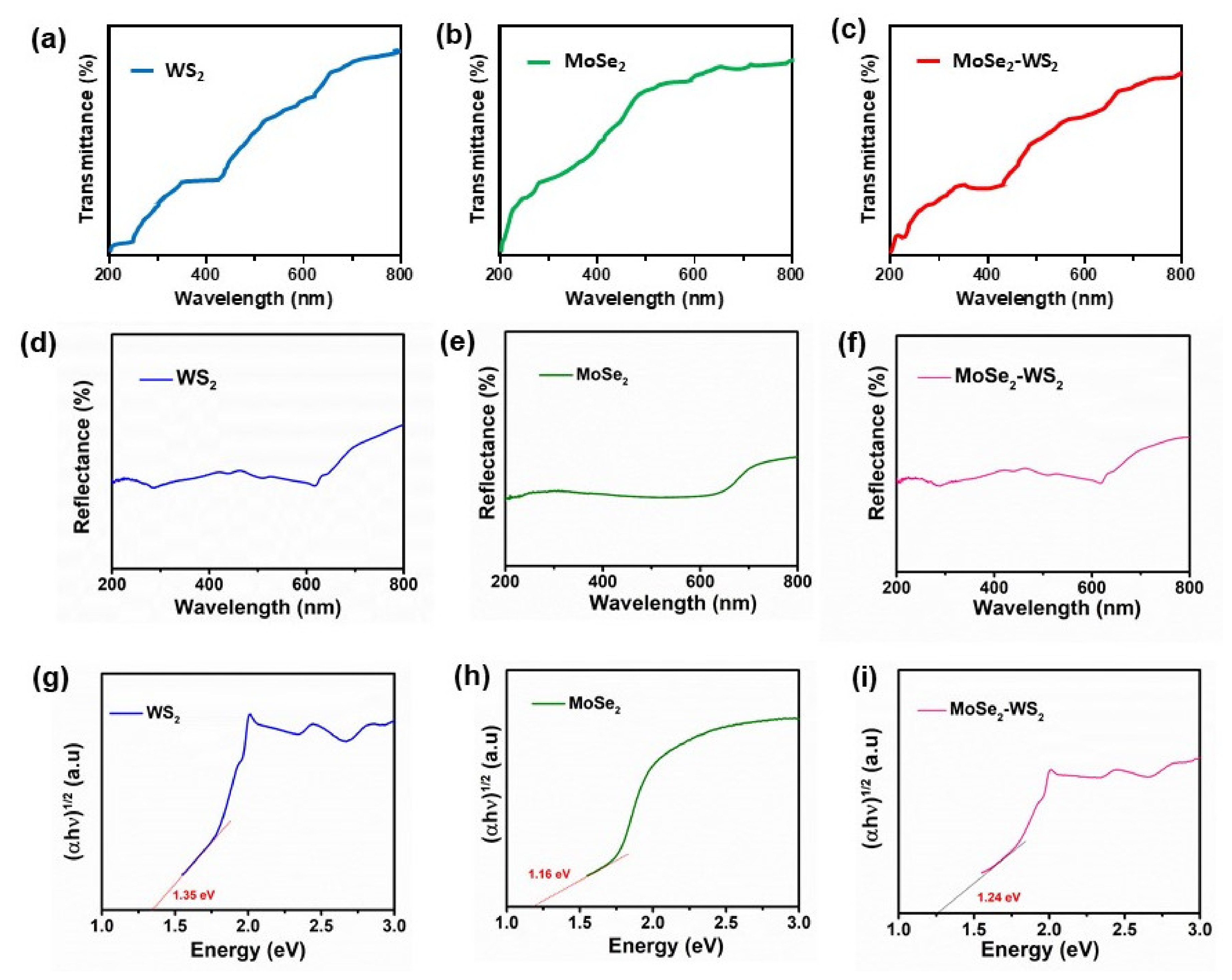
3.6. Optical Studies
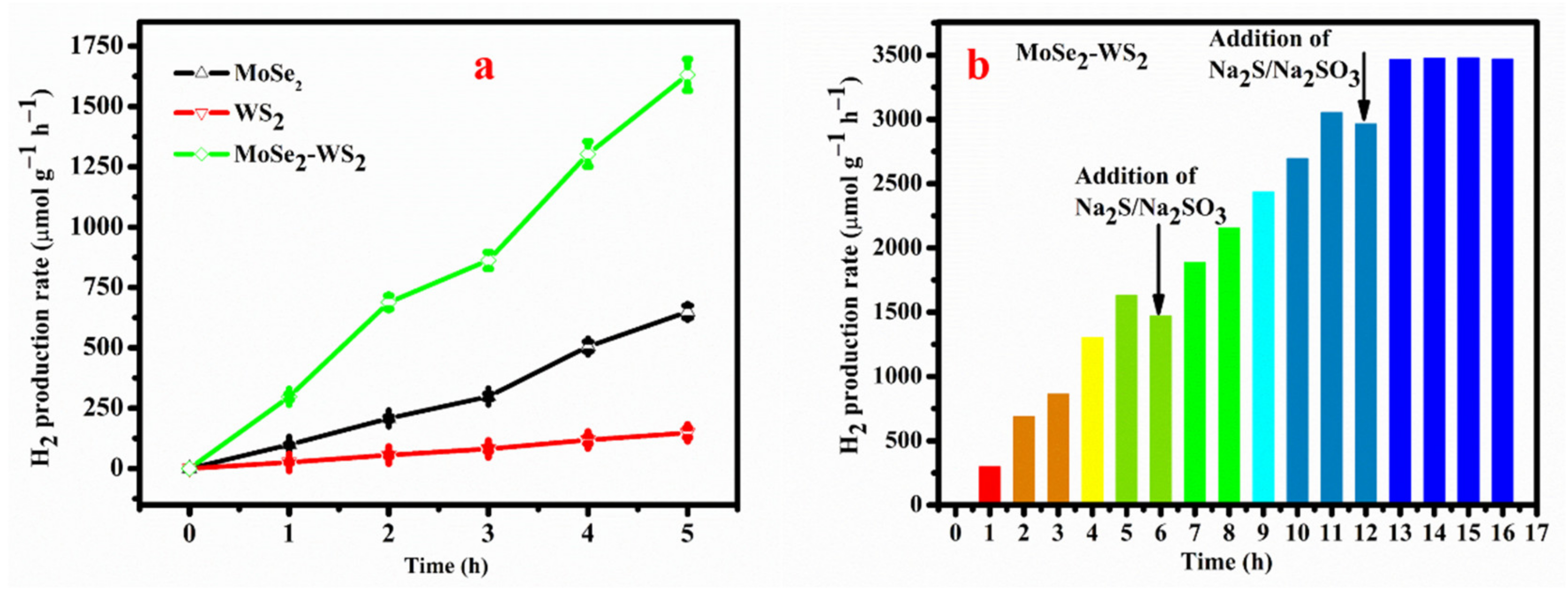
3.7. Photocatalytic Performance
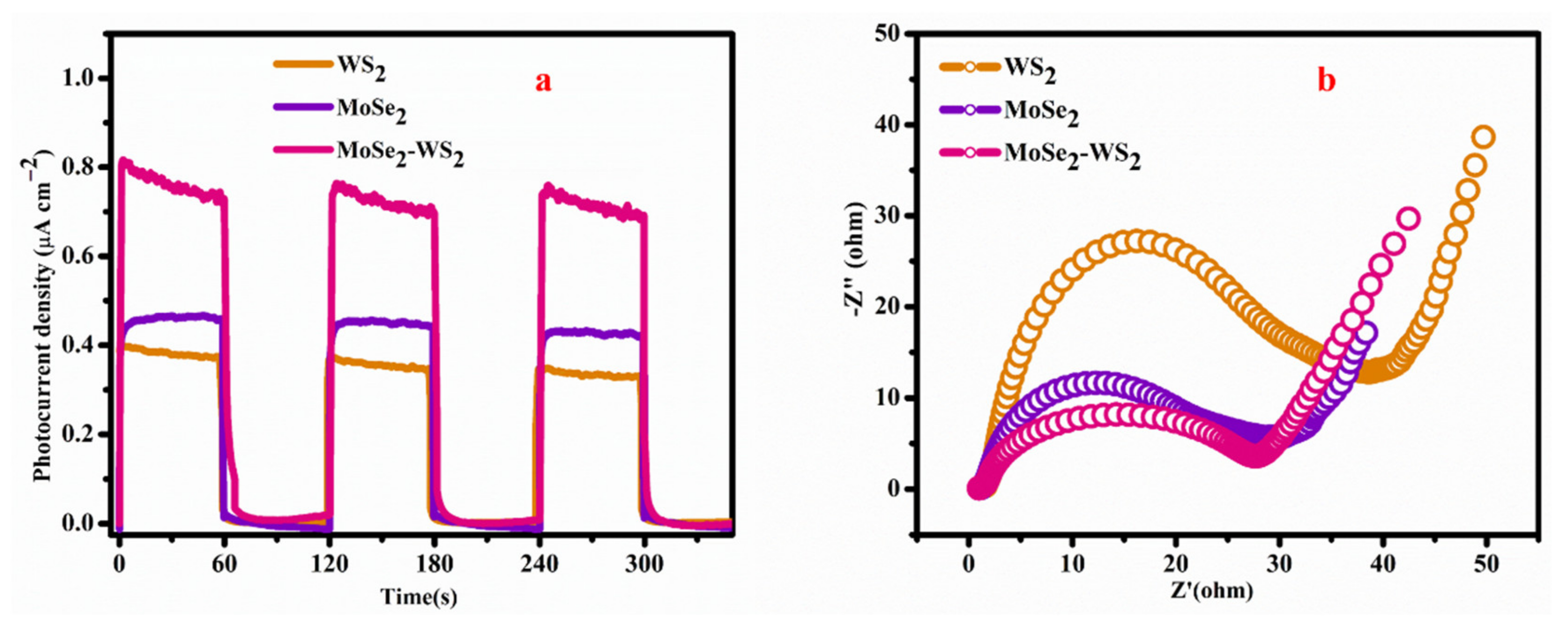
3.8. Electrochemical Performance
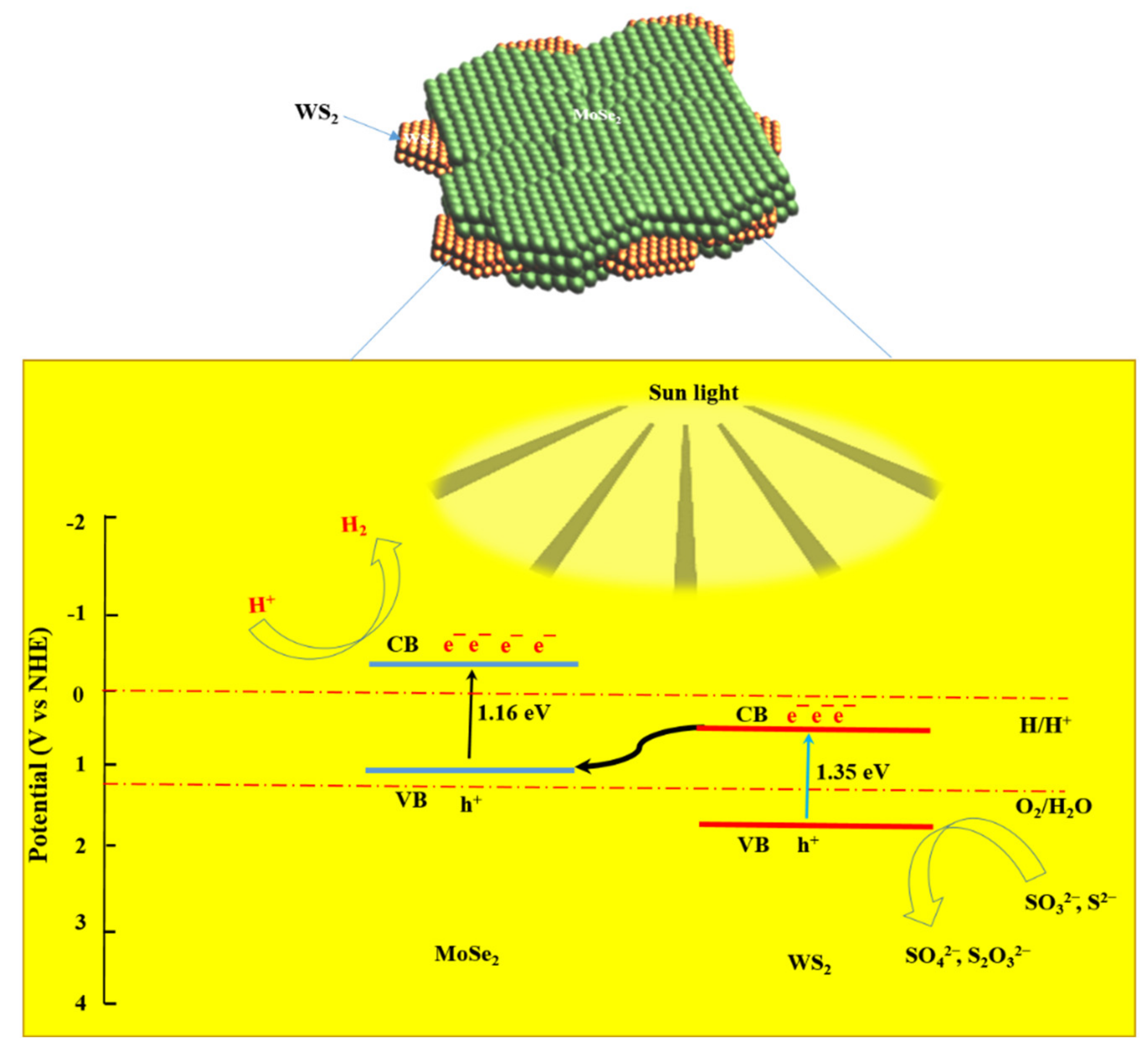
3.9. Proposed Photocatalytic H2 Mechanism
4. Conclusions
- (1)
- A cost-effective and simple chemical methodology was handled to fabricate the MoSe2-WS2 nanostructure using an easy one-step hydrothermal process without high-temperature annealing;
- (2)
- The MoSe2-WS2 nanocomposite has a high specific surface area of 132.79 m2 g−1 and a pore size of 10.6 nm, which are values favorable for an efficient photocatalytic activity. For the MoSe2-WS2 heterostructure, in which WS2 is the core of the sample (bulk) and MoSe2 is formed by a few nanosheets covering the bulk, the evaluated optical bandgap is 1.24 eV;
- (3)
- The use of MoSe2 and WS2 sheets with similar lattice parameters allows the fabrication of heterostructure without matching restriction;
- (4)
- The coupling of MoSe2 with WS2 led to a considerably enhanced surface area and higher photoinduced charge separation. It results a remarkably improved photocatalytic H2 production, which was observed by photocurrent measurements and EIS studies;
- (5)
- Therefore, the resultant MoSe2-WS2 is a capable photocatalyst for the H2 energy applications. Under LED light irradiation, the MoSe2-WS2 nanostructure demonstrated enhanced photocatalytic hydrogen evolution, which is approximately 3- and 10-times higher compare to bare MoSe2 and WS2. MoSe2-WS2 nanocomposite exhibits a high PHE rate of 1600 µmol g−1 h−1;
- (6)
- The photocatalytic activity of the MoSe2-WS2 nanostructure can be explained by Z-scheme carrier transfer pathways, which favor the production of reactive species;
- (7)
- The MoSe2/WS2 heterostructure displayed excellent electrocatalytic hydrogen evolution behavior. The demonstrated hydrogen evolution reaction performance attests to the capability of this nanohybrid to replace the high-cost and scarce Pt and will spark hybrid-based research toward the various future energy sectors. The edges of MoSe2 and WS2 present an ideal hydrogen-binding energy, which makes them promising to replace the Pt-based electrocatalysts for hydrogen generation. In addition, the MoSe2/WS2 heterostructure could be a new cost-effective electrode replacing carbon supported Pt and Pt/Ru electrodes in fuel cells.
Author Contributions
Funding
Institutional Review Board Statement
Informed Consent Statement
Data Availability Statement
Conflicts of Interest
References
- Peng, W.; Li, Y.; Hang, F.; Zhang, G.; Fan, X. Roles of two-dimensional transition metal dichalcogenides as cocatalysts in photocatalytic hydrogen evolution and environmental remediation. Ind. Eng. Chem. Res. 2017, 56, 4611–4626. [Google Scholar] [CrossRef]
- Wang, F.; Shifa, T.A.; Zhan, X.; Huang, Y.; Liu, K.; Cheng, Z.; Jiang, C.; He, J. Recent advances in transition-metal dichalcogenide based nanomaterials for water splitting. Nanoscale 2015, 7, 19764–19788. [Google Scholar] [CrossRef] [PubMed]
- Voiry, D.; Yang, J.; Chhowalla, M. Recent strategies for improving the catalytic activity of 2D TMD nanosheets toward the hydrogen evolution reaction. Adv. Mater. 2016, 28, 6197–6206. [Google Scholar] [CrossRef] [PubMed]
- Mishra, A.K.; Lakshmi, K.V.; Huang, L. Eco-friendly synthesis of metal dichalcogenides nanosheets and their environmental remediation potential driven by visible light. Sci. Rep. 2015, 5, 15718. [Google Scholar] [CrossRef] [PubMed] [Green Version]
- Gopannagari, M.; Kumar, D.P.; Reddy, D.A.; Hong, S.; Song, M.I.; Kim, T.K. In situ preparation of few-layered WS2 nanosheets and exfoliation into bilayers on CdS nanorods for ultrafast charge carrier migrations toward enhanced photocatalytic hydrogen production. J. Catalys. 2017, 351, 153–160. [Google Scholar] [CrossRef]
- Shanker, G.S.; Biswas, A.; Ogale, S. 2D materials and their heterostructures for photocatalytic water splitting and conversion of CO2 to value chemicals and fuels. J. Phys. Energy 2021, 3, 022003. [Google Scholar] [CrossRef]
- Ghatak, K.; Kang, K.N.; Yang, E.; Datta, D. Controlled edge dependent stacking of WS2-WS2 homo- and WS2-WSe2 hetero-structures: A computational study. Sci. Rep. 2020, 10, 1648. [Google Scholar] [CrossRef]
- Thiehmed, Z.; Shakoor, A.; Altahtamouni, T. Recent advances in WS2 and its based heterostructures for water-splitting applications. Catalysts 2021, 11, 1283. [Google Scholar] [CrossRef]
- Wu, Y.; Liu, Z.; Li, Y.; Chen, J.; Zhu, X.; Na, P. Construction of 2D-2D TiO2 nanosheet/layered WS2 heterojunctions with enhanced visible-light-responsive photocatalytic activity. Chin. J. Catalys. 2019, 40, 60–69. [Google Scholar] [CrossRef]
- Wei, Z.; Huang, W.; Xu, L.; Hu, W.; Peng, P.; Huang, G. Dual functions of 2D WS2 and MoS2–WS2 monolayers coupled with a Ag3PO4 photocatalyst. Semicond. Sci. Technol. 2016, 31, 9. [Google Scholar] [CrossRef]
- Jeevanandham, G.; Vediappan, K.; Alothman, Z.A.; Altalhi, T.; Sundramoorthy, A.K. Fabrication of 2D-MoSe2 incorporated NiO Nanorods modified electrode for selective detection of glucose in serum samples. Sci. Rep. 2021, 11, 13266. [Google Scholar] [CrossRef] [PubMed]
- Zhou, Y.; Zhu, Y.; Chen, X.; Dong, B.; Li, Q.; Chai, Y. Carbon-based transition metal sulfides/selenides nanostructures for electrocatalytic water splitting. J. Alloy. Compd. 2021, 852, 156810. [Google Scholar] [CrossRef]
- Qi, S.; Liu, X.; Ma, N.; Xu, H. Construction and photocatalytic properties of WS2/MoS2/BiOCl heterojunction. Chem. Phys. Lett. 2021, 763, 138203. [Google Scholar] [CrossRef]
- Ho, W.; Yu, J.C.; Lin, J.; Yu, J.; Li, P. Preparation and photocatalytic behavior of MoS2 and WS2 nanocluster sensitized TiO2. Langmuir 2004, 20, 5865–5869. [Google Scholar] [CrossRef]
- Tan, C.; Zhang, H. Two-dimensional transition metal dichalcogenide nanosheet-based composites. Chem. Soc. Rev. 2015, 44, 2713–2731. [Google Scholar] [CrossRef]
- Lu, Q.; Yu, Y.; Ma, Q.; Chen, B.; Zhang, H. 2D transition-metal dichalcogenide-nanosheet-based composites for photocatalytic and electrocatalytic hydrogen evolution reactions. Adv. Mater. 2016, 28, 1917–1933. [Google Scholar] [CrossRef]
- Amin, B.; Kaloni, T.P.; Schreckenbach, G.; Freund, M.S. Materials properties of out-of-plane heterostructures of MoS2-WSe2 and WS2-MoSe2. Appl. Phys. Lett. 2016, 108, 063105. [Google Scholar] [CrossRef] [Green Version]
- Ruiz-Tijerina, D.A.; Fal’ko, V.I. Interlayer hybridization and moiré superlattice minibands for electrons and excitons in heterobilayers of transition-metal dichalcogenides. Phys. Rev. B 2019, 99, 125424. [Google Scholar] [CrossRef] [Green Version]
- Jin, C.; Ma, E.Y.; Karni, O.; Regan, E.C.; Wang, F.; Heinz, T.F. Ultrafast dynamics in van der Waals hererostructures. Nat. Technol. 2018, 13, 994–1003. [Google Scholar]
- Kozawa, D.; Carvalho, A.; Verzhbitskiy, I.; Giustiniano, F.; Miyauchi, Y.; Mouri, S.; Castro Neto, A.H.; Matsuda, K.; Eda, G. Evidence for fast interlayer energy transfer in MoSe2/WS2 heterostructures. Nano Lett. 2016, 16, 4087–4093. [Google Scholar] [CrossRef] [Green Version]
- Meng, Y.; Wang, T.; Jin, C.; Li, Z.; Miao, S.; Lian, Z.; Taniguchi, T.; Watanabe, K.; Song, F.; Shi, S.F. Electrical switching between exciton dissociation to exciton funneling in MoSe2/WS2 heterostructure. Nat. Commun. 2020, 11, 2640. [Google Scholar] [CrossRef] [PubMed]
- Amin, B.; Kaloni, T.P.; Schwingenschlögl, U. Strain engineering of WS2, WSe2, and WTe2. RSC Adv. 2014, 4, 34561–34565. [Google Scholar] [CrossRef]
- Ceballos, F.; Ju, M.G.; Lane, S.D.; Zeng, X.C.; Zhao, H. Highly efficient and anomalous charge transfer in van der Waals trilayer semiconductors. Nano Lett. 2017, 17, 1623–1628. [Google Scholar] [CrossRef] [PubMed]
- Wu, Z.; Ouyan, M.; Wang, D. Construction of WS2/MoSe2 heterojunction for efficient photoelectrocatalytic hydrogen evolution. Mater. Sci. Semicond. Process 2020, 107, 104822. [Google Scholar] [CrossRef]
- Jaramillo, T.F.; Jørgensen, K.P.; Bonde, J.; Nielsen, J.H.; Horch, S.; Chorkendorff, I. Identification of active edge sites for electrochemical H2 evolution from MoS2 nanocatalysts. Science 2007, 317, 100–102. [Google Scholar] [CrossRef] [Green Version]
- Kang, J.; Tongay, S.; Zhou, J.; Li, J.; Wu, J. Band offsets and heterostructures of two-dimensional semiconductors. Appl. Phys. Lett. 2013, 102, 012111. [Google Scholar] [CrossRef] [Green Version]
- Vikraman, D.; Hussain, S.; Truong, L.; Karuppasamy, K.; Kim, H.J.; Maiyalagan, T.; Chun, S.H.; Jung, J.; Kim, H.S. Fabrication of MoS2/WSe2 heterostructures as electrocatalyst for enhanced hydrogen evolution reaction. Appl. Surf. Sci. 2019, 480, 611–620. [Google Scholar] [CrossRef]
- Vikraman, D.; Hussain, S.; Patil, S.A.; Truong, L.; Arbab, A.A.; Jeong, S.H.; Chun, S.H.; Jung, J.; Kim, H.-S. Engineering MoSe2/WS2 hybrids to replace the scarce platinum electrode for hydrogen evolution reactions and dye-sensitized solar cells. ACS Appl. Mater. Interfaces 2021, 123, 5061–5072. [Google Scholar] [CrossRef]
- Yuan, Z.; Jiang, Q.; Feng, C.; Chen, X.; Guo, Z. Synthesis and performance of tungsten disulfide/carbon (WS2/C) composite as anode material. J. Electron. Mater. 2018, 47, 251–260. [Google Scholar] [CrossRef]
- Xiong, M.; Qian, J.; Yang, K.; Chen, Z.; Mei, T.; Wang, J.; Li, J.; Yu, L.; Wang, X. Efficient polysulfide anchor: Brain coral-like WS2 nanosheets. J. Mater. Sci. 2020, 55, 12031–12040. [Google Scholar] [CrossRef]
- Zhao, Y.; Liu, J.; Zhang, X.; Wang, C.; Zhao, X.; Li, J.; Jin, H. Convenient synthesis of WS2–MoS2 heterostructures with enhanced photocatalytic performance. J. Phys. Chem. C 2019, 123, 27363–27368. [Google Scholar] [CrossRef]
- Eftekhari, A. Molybdenum diselenide (MoSe2) for energy storage, catalysis, and optoelectronics. Appl. Mater. Today 2017, 8, 1–17. [Google Scholar] [CrossRef]
- Peng, K.; Wang, H.; Li, X.; Wang, J.; Cai, Z.; Su, L.; Fan, X. Emerging WS2/montmorillonite composite nanosheets as an efficient hydrophilic photocatalyst for aqueous phase reactions. Sci. Rep. 2019, 9, 16325. [Google Scholar] [CrossRef] [PubMed]
- Vaziri, H.S.; Shokuhfar, A.; Afghah, S.S.S. Synthesis of WS2/CNT hybrid nanoparticles for fabrication of hybrid aluminum matrix nanocomposite. Mater. Res. Express 2020, 7, 025034. [Google Scholar] [CrossRef]
- Li, X.; Peng, K. MoSe2/montmorillonite composite nanosheets: Hydrothermal synthesis, structural characteristics, and enhanced photocatalytic activity. Minerals 2018, 8, 268. [Google Scholar] [CrossRef] [Green Version]
- Zeng, P.; Ji, X.; Su, Z.; Zhang, S. WS2/g-C3N4 composite as an efficient heterojunction photocatalyst for biocatalyzed artificial photosynthesis. RSC Adv. 2018, 8, 20557–20567. [Google Scholar] [CrossRef] [Green Version]
- Gusakova, J.; Wang, X.; Shiau, L.L.; Krivosheeva, A.; Shaposhnikov, V.; Borisenko, V.; Gusakov, V.; Tay, B.K. Electronic properties of bulk and monolayer TMDs: Theoretical study within DFT framework (GVJ-2e method). Phys. Status Solidi A 2017, 214, 1700218. [Google Scholar] [CrossRef]
- Rusu, D.I.; Rusu, G.G.; Luca, D. Structural characteristics and optical properties of thermally oxidized zinc films. Acta Phys. Polonica A 2011, 119, 850–856. [Google Scholar] [CrossRef]
- Tauc, J. Optical Properties of Solids; Abeles, F., Ed.; North-Holland: Amsterdam, The Netherlands, 1972. [Google Scholar]
- Zanatta, A.R. Revisiting the optical bandgap of semiconductors and the proposal of a unified methodology to its determination. Sci. Rep. 2019, 9, 11225. [Google Scholar] [CrossRef] [Green Version]
- Yoffe, A.D. Low-dimensional systems: Quantum size effects and electronic properties of semiconductor microcrystallites (zero-dimensional systems) and some quasi-two-dimensional systems. Adv. Phys. 1993, 42, 173–266. [Google Scholar] [CrossRef]
- Wang, Q.H.; Kalantar-Zadeh, K.; Kis, A.; Coleman, J.N.; Srano, M.S. Electronics and optoelectronics of two-dimensional transition metal dichalcogenides. Nat. Nanotechnol. 2012, 7, 699–712. [Google Scholar] [CrossRef] [PubMed]
- Ding, Y.; Wang, Y.; Ni, J.; Shi, L.; Shi, S.; Tang, W. First principles study of structural, vibrational and electronic properties of graphene-like MX2 (M=Mo, Nb, W, Ta; X=S, Se, Te) monolayers. Phys. B 2011, 406, 2254–2260. [Google Scholar] [CrossRef]
- Police, A.K.R.; Vattikuti, S.V.P.; Mandari, K.K.; Chennaiahgari, M.; Sharma, P.; Vallurid, D.K.; Byon, C. Bismuth oxide cocatalyst and copper oxide sensitizer in Cu2O/TiO2/Bi2O3 ternary photocatalyst for efficient hydrogen production under solar light irradiation. Ceram. Int. 2018, 44, 11783–11791. [Google Scholar] [CrossRef]
- Maeda, K. Z-scheme water splitting using two different semiconductor photocatalysts. ACS Catal. 2013, 3, 1486–1503. [Google Scholar] [CrossRef]
- Wang, G.; Chang, J.; Tang, W.; Xie, W.; Ang, Y.S. 2D materials and heterostructures for photocatalytic water-splitting: A theoretical perspective. J. Phys. D Appl. Phys. 2022, 5, 293002. [Google Scholar] [CrossRef]
- Fu, C.; Wang, G.; Huang, Y.; Chen, Y.; Yuan, H.; Ang, Y.S.; Chen, H. Two-dimensional CdS/SnS2 heterostructure: A highly efficient direct Z-scheme water splitting photocatalyst. Phys. Chem. Chem. Phys. 2022, 24, 3826–3833. [Google Scholar] [CrossRef] [PubMed]
- Cui, L.; Xiang Ding, X.; Wang, Y.; Shi, H.; Huang, L.; Zuo, Y.; Kang, S. Facile preparation of Z-scheme WO3/g-C3N4 composite photocatalyst with enhanced photocatalytic performance under visible light. Appl. Surface Sci. 2017, 391, 202–210. [Google Scholar] [CrossRef]


| Sample | BET Surface Area (m2 g−1) | Pore Volume (cm3 g−1) | Pore Size (nm) |
|---|---|---|---|
| WS2 | 106.2 | 0.214 | 10.7(2) |
| MoSe2 | 35.07 | 0.11 | 8.3(2) |
| MoSe2-WS2 | 132.8 | 0.268 | 10.6(5) |
Publisher’s Note: MDPI stays neutral with regard to jurisdictional claims in published maps and institutional affiliations. |
© 2022 by the authors. Licensee MDPI, Basel, Switzerland. This article is an open access article distributed under the terms and conditions of the Creative Commons Attribution (CC BY) license (https://creativecommons.org/licenses/by/4.0/).
Share and Cite
Padma, T.; Gara, D.K.; Reddy, A.N.; Vattikuti, S.V.P.; Julien, C.M. MoSe2-WS2 Nanostructure for an Efficient Hydrogen Generation under White Light LED Irradiation. Nanomaterials 2022, 12, 1160. https://doi.org/10.3390/nano12071160
Padma T, Gara DK, Reddy AN, Vattikuti SVP, Julien CM. MoSe2-WS2 Nanostructure for an Efficient Hydrogen Generation under White Light LED Irradiation. Nanomaterials. 2022; 12(7):1160. https://doi.org/10.3390/nano12071160
Chicago/Turabian StylePadma, Tatiparti, Dheeraj Kumar Gara, Amara Nadha Reddy, Surya Veerendra Prabhakar Vattikuti, and Christian M. Julien. 2022. "MoSe2-WS2 Nanostructure for an Efficient Hydrogen Generation under White Light LED Irradiation" Nanomaterials 12, no. 7: 1160. https://doi.org/10.3390/nano12071160
APA StylePadma, T., Gara, D. K., Reddy, A. N., Vattikuti, S. V. P., & Julien, C. M. (2022). MoSe2-WS2 Nanostructure for an Efficient Hydrogen Generation under White Light LED Irradiation. Nanomaterials, 12(7), 1160. https://doi.org/10.3390/nano12071160