Abstract
Molybdenum disulfide (MoS2) got tremendous attention due to its atomically thin body, rich physics, and high carrier mobility. The controlled synthesis of large area and high crystalline monolayer MoS2 nanosheets on diverse substrates remains a challenge for potential practical applications. Synthesizing different structured MoS2 nanosheets with horizontal and vertical orientations with respect to the substrate surface would bring a configurational versatility with benefit for numerous applications, including nanoelectronics, optoelectronics, and energy technologies. Among the proposed methods, ambient pressure chemical vapor deposition (AP-CVD) is a promising way for developing large-scale MoS2 nanosheets because of its high flexibility and facile approach. Here, we show an effective way for synthesizing large-scale horizontally and vertically aligned MoS2 on different substrates such as flat SiO2/Si, pre-patterned SiO2 and conductive substrates (TaN) benefit various direct TMDs production. In particular, we show precise control of CVD optimization for yielding high-quality MoS2 layers by changing growth zone configuration and the process steps. We demonstrated that the influence of configuration variability by local changes of the S to MoO3 precursor positions in the growth zones inside the CVD reactor is a key factor that results in differently oriented MoS2 formation. Finally, we show the layer quality and physical properties of as-grown MoS2 by means of different characterizations: Raman spectroscopy, scanning electron microscopy (SEM), photoluminescence (PL) and X-ray photoelectron spectroscopy (XPS). These experimental findings provide a strong pathway for conformally recasting AP-CVD grown MoS2 in many different configurations (i.e., substrate variability) or motifs (i.e., vertical or planar alignment) with potential for flexible electronics, optoelectronics, memories to energy storage devices.
1. Introduction
Over the last decade, transition metal dichalcogenides (TMDs) have attracted immense interest because of their outstanding electrical, optical and chemical properties [1,2,3]. These TMDs are typically attributed as MX2, where M is a transition metal atom (i.e., molybdenum, Mo) and X refers to a chalcogen atom (i.e., sulfur, S) to form a TMD (i.e., molybdenum disulfide, MoS2). Monolayer MoS2, with a direct band gap of 1.8 eV and a three atoms thick nanosheet, shows potential applications in the fields of electronics, optoelectronics and valleytronics due to optical transparency, high carrier mobility, no-dangling bonds and atomically thickness [3,4,5]. In addition, conformal growth of MoS2 nanosheets over pre-patterned substrates enables an added advantage for effective routes towards fabrication; the miniaturization of integrated circuits and structurally excellent TMD materials are essential for flexible optoelectronics such as LEDs and may lead to bandgap and exciton engineering through local strain generation due to excellent conformal growth and layer bendability [6,7]. The growth on the patterned substrate is also fundamental for the exploitation of the anisotropy by design in MoS2 and related TMDs, thus enabling the engineering of the electronic band structure as a function of the local strain. Anisotropic effects are relevant in a broad range of applications. For instance, when we consider the resulting nanosheets as 2D rippled membranes, we are devising new physical concepts to enhance the optical, plasmonic, and catalytic performance of the pristine materials. Further, direct growth on engineered patterned substrates promotes strain engineering, with implications on relevant properties of TMDs such as the thermal/electronic transport or the exciton physics, which are dramatically affected by the anisotropy-dependent degree of strain [8,9]. On another front, direct growth of high crystalline MoS2 on conductive substrates would open up a new pathway for easy integration in memory devices by serving as a bottom electrode and also providing an underlying conductive substrate [10]. MoS2 and other TMDs, such as TaS2, are considered as diffusion barriers in ultra-scaled microelectronics (<5 nm technology node) directly in contact with TaN or Cu, which are commonly used as interconnects in back-end-of-line compatible processes [11,12]. In this regard, a significant demand to develop an efficient approach to direct growth of MoS2 on metal or conductive substrates at a large scale is still demanding, although the high process temperature poses severe constraints in terms of substrate stability during growth. In contrast, multilayered MoS2 with an indirect band gap of 1.3 eV, disordered structures with exposed edge defects, chemical stability and high surface area are a favorable ground for heterogeneous catalysis reaction with promising impact on hydrogen storage and fuel cells [4,13,14,15]. It is known that excellent catalytic activities of MoS2 are greatly enhanced by using conductive layers as a growth substrate, thus providing cost-effective, high-performance catalysts in electrocatalysis over Pt [13].
Before the practical applications, so far, several considerable efforts have been focused on the preparation of large-scale MoS2. Approaches, such as physical and chemical exfoliation, chemical synthesis, atomic layer deposition, laser annealing, physical vapor deposition and chemical vapor deposition, have been reported [16,17,18,19]. Among the proposed methods, chemical and mechanical exfoliation, physical vapor deposition, and chemical vapor deposition schemes are the most used ones [18,20]. Specifically, chemical exfoliation or sonication are versatile methods for the low cost, scalable production of monolayer 2D materials [16,21]. Mechanical, or tape, exfoliation allows to obtain high crystal quality of monolayer MoS2 but is beneficial for fundamental property studies only [17]. Indeed, small size, nonuniform thickness and agglomeration in solution are drawbacks of this method. An explicit understanding of these variables is critical for precise control of MoS2 morphology with large coverage during their growth. Such desired knowledge could further allow for the synthesis of other TMDs that consists of both vertical and horizontally grown layer structures [22].
Ambient pressure chemical vapor deposition (AP-CVD) is a facile, efficient, scalable method to grow large-scale monolayer MoS2 aiming for the fabrication of integrated devices [23,24]. Conversely, CVD is also a flexible, cost-effective, and scalable process for growth optimization from flat horizontal to vertically oriented structured MoS2 for energy storage applications. Despite atomically thin MoS2 have been successfully grown on SiO2/Si, also by our research team, [24] there are still some limitations in extending this process to direct synthesis of large-area monolayers on different substrates such as pre-patterned and metal or conductive substrates. In this respect, computational studies, based on ab-initio methods, such as density functional theory, provided useful insights in predicting and clarifying the growth mechanism involved in CVD growth of TMDs and similar systems [25,26,27]. Having the application target in mind, precise tuning of the growth orientations of horizontally and vertically aligned MoS2 is critically important to benefit from their tailored materials properties and device functionalities in various fields. Furthermore, by modifying the configurational design inside the CVD reactor, the direct growth of large-scale MoS2 on any arbitrary conductive substrate would open up an easy route for bottom contacts, thus facilitating MoS2 integration in devices.
In this work, we investigated the growth behavior of mono to a few layers of MoS2 from molybdenum trioxide (MoO3) and sulfur (S) solid powders as a precursor in the AP-CVD process. We explicitly demonstrated the local changes of the S to MoO3 precursor positions in the growth zone inside the CVD reactor, which play a key factor in the changing of MoS2 nanosheets orientation. We successfully synthesized high-quality MoS2 flat monolayers and vertically aligned bulk MoS2 up to cm2 scale with good uniformity on different substrates such as SiO2/Si, pre-patterned SiO2 and TaN. In addition, we grew isolated single domains to continuous MoS2 conformally on the pre-patterned surface without any ruptures. The growth formation, crystallinity, extension of monolayer and vertically grown MoS2 layers were characterized by a series of techniques such as Raman spectroscopy, X-ray photoelectron spectroscopy (XPS), scanning electron microscopy (SEM) and photoluminescence (PL). We conclude with an outlook on the prospective scientific future of device developments based on MoS2 grown by optimized CVD methods.
2. Materials and Methods
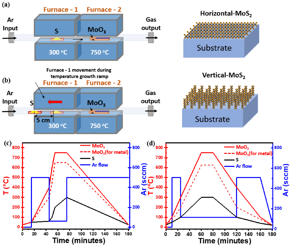
MoS2 nanosheets reported in this work has been grown using atmospheric-pressure chemical vapor deposition (AP-CVD), in which powder of sulfur (S, 99.98%, Sigma-Aldrich, Darmstadt, Germany) and molybdenum trioxide (MoO3, 99.97%, Sigma-Aldrich, Darmstadt, Germany) were used as precursor sources. Amorphous SiO2(50 nm)/Si (100) substrates were utilized for initial MoS2 growth experiments. Furthermore, we extended our optimized growth recipe to pre-patterned SiO2 and tantalum nitride (TaN) substrates. The growth procedure takes place inside a two-zone-furnace AP-CVD apparatus with a 2” quartz tube with a length of 150 cm where upstream (S) and downstream (MoO3) containing boats are precisely positioned, as shown in Figure 1a. For the synthesis of horizontal and vertical aligned films, a similar setup was used but with some changes, as detailed in individual sections below.
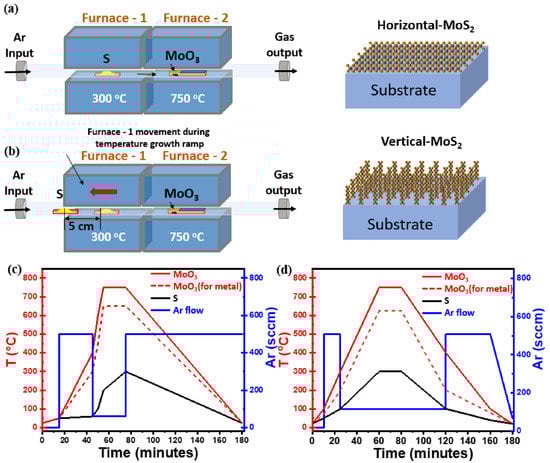
Figure 1.
(a) Schematic diagram of the horizontal two-zone CVD furnace for the synthesis of flat-MoS2. (b) Modified CVD setup used to synthesize vertical-MoS2 nanosheets by adjusting the boat position during the growth temperature ramp on different substrates (c) Different steps of temperature profile (left y-axis) adopted for the synthesis of flat-MoS2 nanosheets with growth ramp at 750 °C (solid line, SiO2/Si) and 650 °C (dash line, TaN) for 20 min; in the same graph the Ar flux changes during the CVD process are also plotted (blue solid line, right y-axis). (d) Three step temperature profile (left y-axis) used for the synthesis of vertical-MoS2 nanosheets with growth ramp at 750 °C (solid line, SiO2/Si) and 625 °C (dash line, TaN) for 20 min; in the same graph the Ar flux changes during the CVD process are also plotted (blue solid line, right y-axis).
Synthesis of Horizontally Aligned MoS2 Nanosheets
During the CVD, S and MoO3 powders with the amount of 200 mg and 1 mg, respectively, were contained in crucibles and placed near to heating zones of upstream and downstream furnaces. A SiO2(50 nm)/Si substrate previously cleaned was kept face-down above the MoO3 containing crucible. Substrate cleaning was performed with acetone and isopropanol followed by immersion in piranha solution of composition H2O2:H2SO4 (1:3) for 2 h to make the surface hydrophilic, rinsed with deionized water and finally N2 blown to dry. Following the previous steps, the substrate was conditioned with PTAS (Perylene-3,4,9,10-tetracarboxylic acid tetrapotassium salt) seeding promotor, 0.29 mg mixed in 10 mL distilled water solution, dropped on the clean SiO2/Si substrate using micropipette, then spun at 600 rpm for 60 s. The use of PTAS molecules as a seed promotor during the process of substrate conditioning has been demonstrated to improve the size of MoS2 nanodomains and the overall MoS2 nanosheets synthesis by promoting lateral flat growth at the expense of the “3D-like” vertical growth [24,28]. In other words, without PTAS, we could not reach satisfactory surface coverage; the 2D-like MoS2 domains are small in size, less than 10 μm, and they are isolated, leaving a relevant region of the exposed substrate surface with no MoS2 growth, as shown in representative SEM image in Figure S1 in Supplementary Materials (SM). The S and MoO3 containing boats are placed in the middle of each heat zone of the furnace, as shown in the schematic in Figure 1a. The temperature profile during the 2 h long CVD process reaches a maximum of 300 °C for sulfur and 750 °C for MoO3 during the effective growth step of 20 min; concomitantly, Ar flux varies from 60 sccm, during the 20 min growth time, to 500 sccm in the other different steps during the CVD process, as shown in Figure 1c. The temperature profile for S, with a maximum temperature of 300 °C, grants the control of the sulfur sublimation rate. For the MoO3-containing furnace, 750 °C is selected to facilitate the chemical reactivity of Mo at the sample surface while avoiding the formation of MoSxOy by-products. In the case of TaN substrates, we reduced the growth temperature to 650 °C in the MoO3 heating zone to preserve TaN from evaporation, as shown in Figure 1c (dashed line). The temperature profile for S was kept identical to the case of SiO2/Si substrate, while the Ar flux varied from 100 sccm during the effective growth step up to 600 sccm in the other steps.
Synthesis of Vertically Aligned MoS2 Nanosheets
In the case of vertically aligned MoS2, we used S and MoO3 powders in the amount of 300 mg and 1 mg, respectively, as we modified the apparatus setup according to the growth conditions. Here it is worth noting that, during the sample conditioning, we do not make use of any seeding promotor. Initially, we positioned the sulfur source at the beginning of the heat zone, far from (downstream) furnace 1, to prevent any pre-evaporation of sulfur, as shown in Figure 1b. The MoO3 source, along with the downface substrate, is placed at the centre of the heat zone in the (upstream) furnace 2. Once the MoO3 containing furnace reaches the maximum of the ramping up temperature, namely 750 °C, we slowly introduce the sulfur vapors by moving the S furnace 1 (S temperature zone) manually towards the molybdenum direction and releasing the Ar carrier gas of 100 sccm. In this growth method, the carrier gas flow is kept low and constant for a long time during some CVD process steps. The delayed introduction of the sulfur source together with its high excess at the position where the chemical reaction between the MoO3 and S happens creates a concentration gradient normal to the substrate surface, promoting the out-of-plane vertical growth of MoS2 possibly due to the Mullins–Sekerka mechanism, thus ultimately leading to vertical oriented MoS2 growth, as mentioned in the literature [22,29]. Here, the delayed reaction takes place in vapor phase between the S and MoO3. In addition, the absence of seed promotors during the pre-treatment of the substrate surface changes the surface wettability, which is also to be considered a key factor for vertical growth. Figure 1d shows the three steps temperature profile, together with the Ar flux profile, followed during the vertically aligned MoS2 growth. The process starts with the introduction of the source precursors, followed by temperature ramp steps and natural cool down of the apparatus. Differently from the horizontal growth case, here we reduced the growth temperature to 625 °C for TaN substrate to avoid any possible substrate reactivity as indicated by the red dash line in Figure 1d.
Characterization Methods
The morphology of the as-grown samples was first examined by scanning electron microscopy (SEM) using a Zeiss-SUPRA 40 field-emission SEM device (Oberkochen, Germany) in bright field mode. Photoluminescence (PL) and confocal micro-Raman spectroscopy were performed using a Renishaw In-Via spectrometer (New Mills, Kingswood, Wotton-under-Edge, UK) equipped with a solid-state laser source of excitation wavelength 514 nm (2.41 eV) in backscattering configuration. Particular care was put in the laser power, reduced to 5% of the nominal power (i.e., below 1 mW) to avoid sample damage. Complementary PL was acquired with the same Raman equipment by changing the instrument configuration. X-ray photoelectron spectroscopy (XPS) measurements were acquired on a PHI 5600 instrument equipped with a monochromatic Al Kα X-ray source with an energy of 1486.6 eV and a concentric hemispherical analyser. The spectra were collected at a take-off angle of 45° and band-pass energy of 58.70 eV. The instrument resolution was 0.5 eV. The spectra were aligned using C 1s (285 eV) as reference.
3. Results and Discussion
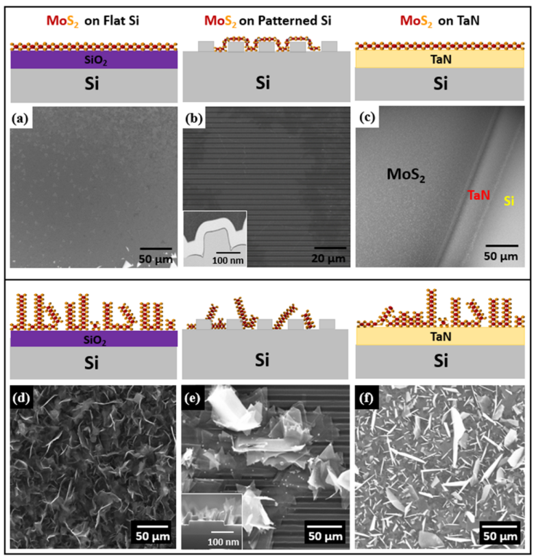
Horizontally and vertically aligned MoS2 were synthesized using a two-zone-furnace CVD apparatus on different substrates such as SiO2/Si, pre-patterned and conductive substrates. Initial experiments were developed on flat SiO2/Si substrates later extended the optimized growth approach to other substrates in terms of flat few layers MoS2. Figure 2a–f represents schematics and SEM images of horizontally and vertically aligned MoS2 on the different substrates. The as-grown MoS2 morphology on flat SiO2/Si in the large region is shown by the SEM image as having a lateral size of more than 200 µm of continuous film, as shown in Figure 2a. Here we observed that the triangular MoS2 domains merge to yield a large-scale uniform single layer. The MoS2 domains are large and tend to connect to each other despite the fact that their orientation on the surface is not controlled. Thus, the amount of grain boundaries and possibly other defects is reduced with respect to the case of relatively small domains randomly oriented in the space. As further evidence, we show large-scale lateral growth of monolayer MoS2 up to a centimeter scale in Figures S2 and S3 in Supplementary Materials. Using the same experimental conditions in CVD, we obtained a large-area continuous monolayer MoS2 on a patterned SiO2/Si substrate (Figure 2b). The cross-sectional view of the monolayer MoS2 is also characterized with transmission electron microscopy (TEM), where we observe that the MoS2 layer conformally follows the trenches of the pre-patterned substrate as also detailed in the inset TEM cross-sectional image in Figure 2b (see also Figure S4 in Supplementary Materials). By optimizing the CVD growth conditions, we also synthesized highly crystalline few-layers MoS2 on TaN. One of the critical parameters during the direct growth of MoS2 on the TaN substrate is the growth temperature because of the lower TaN evaporation temperature with respect to the MoS2 growth temperature. Although it is well documented that the chemical reaction from Ta(N) and S to form TaS2 happens at around 900 °C at ambient pressure [30], we could still note a minimal presence of TaS2 phonon modes in Raman measurements, related to the imbalance between the formation of MoS2 and TaS2 in an atmosphere supersaturated in S, as in our case. Here, we controlled the MoO3 temperature by lowering it to 650 °C to preserve TaN film. Figure 2c shows the SEM image of the edge part taken at the interface of MoS2 on TaN with exposed silicon on the bottom. The SEM image reveals the domain structure of large-area, horizontally grown monolayer MoS2 without any vertically-aligned layers, as shown in Figure 2a–c.
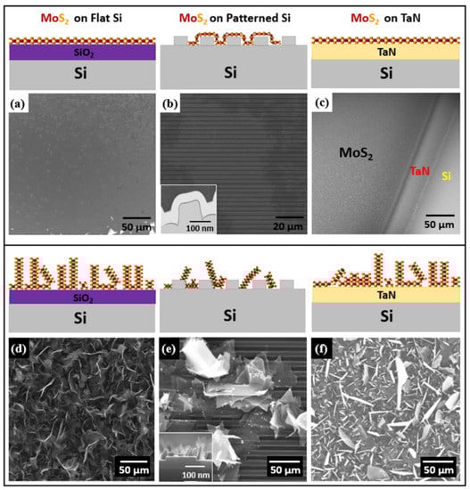
Figure 2.
Schematic illustration of horizontal and vertical growth of MoS2 using AP-CVD and SEM image (a) large area monolayer MoS2 grown on flat SiO2/Si substrate (b) isolated flake of flat monolayer MoS2 domain on patterned SiO2/Si; inset TEM cross sectional image shows conformal monolayer MoS2 growth on patterned trenches (thin dark line). (c) flat MoS2 on TaN. (d–f) vertically standing MoS2 nanosheets (d) on SiO2/Si (e) on pre-patterned substrate, inset: SEM cross section (f) on TaN.
The vertically aligned MoS2 growth was obtained by controlling the insertion of sulfur precursor during the temperature ramping-up stage because of substantial differences in the growth kinetics. In CVD growth, we control the sulfur flow that reaches the MoO3 source by changing the position of the boat containing sulfur with respect to the heat zone furnace in such a way that the kinetics in the sulfur transport acts as the governing factor for the vertical growth orientation. We speculate that during the growth process, intensive compression between the highly dense bulk MoS2 domains leads to the collision with other MoS2 islands, thus causing vertical growth. In the vertical growth regime, the sulfur reaction with MoO3 yields a concentration gradient normal to the substrate at the substrate surface. This event could have a role in promoting the out-of-plane vertical growth of MoS2 due to the Mullins-Sekerka mechanism and significantly reducing the sulfur flow downstream during the growth [22,29]. Figure 2d–f show SEM images of the vertically aligned MoS2 nanosheets grown on different substrates. A uniformly covered MoS2 grown on flat SiO2/Si substrate is clearly shown in Figure 2d. Furthermore, we used the same growth conditions to yield vertical MoS2 nanosheets on patterned substrates. Figure 2e clearly shows the presence of triangular vertical MoS2 domains after the growth. Bulk MoS2 domains appear very bright compared to the few-layers MoS2 domains, an indication of a large density of exposed domain edges. In addition, the cross-sectional SEM image in the inset of Figure 2e demonstrates that the as-grown MoS2 triangular domains are nearly perpendicular to the patterned substrate surface (see also the cross-section SEM image in Figure S5 in Supplementary Materials). Such findings possibly claim a larger density of defects in the grown MoS2 with respect to the flat case. In a simplified picture, in the vertical growth, MoS2 domains are formed at a random orientation each other, possibly promoting a high number of defects at their edges, with the final result that a consistent density of defects would be formed. On the other hand, during the CVD growth on TaN, the critical drawback is to control the TaN evaporation temperature and the transition metal source temperature (i.e., molybdenum). Therefore, we precisely investigated different temperatures to preserve the underlying TaN film. Facilitating the same growth approach with the slightly reduced temperature down to 650 °C, we successfully synthesized MoS2 on TaN, as shown in Figure 2f, where a top view of vertical MoS2/ TaN/SiO2 interface is imaged by SEM. Surprisingly, we observed flakes appearing as bright or dark in the SEM image. This fact may be correlated with the competing formation of TaS2 flakes along with MoS2 as a collateral reaction between S and the TaN substrate according to the observed TaS2-related feature in the Raman spectrum in Figure 4d.
To gain additional characterization to our MoS2 growths, micro-Raman spectroscopy, photoluminescence (PL), and atomic force microscopy (AFM) (Figure S6 in Supplementary Materials) were also employed to probe the structure, optical response and thickness uniformity of flat horizontal MoS2 monolayers as shown in Figure 3a–d.
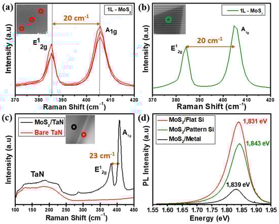
Figure 3.
(a) Raman spectra obtained at different positions on the as-grown horizontal monolayer MoS2 nanosheets on flat SiO2/Si; the inset shows the SEM image with the positions of the Raman measures with red open circles (b) Raman spectrum taken on monolayer MoS2 on pattern substrate; the inset shows the SEM image with the position of the Raman measure with green open circle. (c) Raman spectra of bare TaN substrate (red) and after three layers MoS2 grown on TaN (black); the inset shows the SEM image with the positions of the Raman measures on TaN substrate with red and MoS2 grown on TaN black open circles (d) PL spectra of a MoS2 on flat Si (red), pattern SiO2/Si (green) and TaN (black) substrates.
Figure 3a shows the Raman spectra from MoS2 nanosheets grown on SiO2/Si flat substrate recorded at different positions. The measurements give E12g (in-plane) and A1g (out of plane) phonon modes located at 385.5 and 405.2 cm−1, respectively. The wavelength difference of 19.7 cm−1 confirms the growth of a MoS2 monolayer, consistent with values reported in the literature [31]. Figure 3b shows the Raman measurements on the MoS2 grown on the pre-patterned substrate. The measurement gives the same E12g and A1g phonon modes with a frequency difference of ~20 cm−1, which validates the growth of a monolayer MoS2. As for TaN, we acquired the Raman spectrum of the substrate before and after the MoS2 growth, as shown in Figure 3c. The Raman spectrum from bare TaN (red line in Figure 3c) confirms the crystallinity of TaN with a primary first-order acoustic mode (A) centred near 200 cm−1 [32,33]. The occurrence of slight variations in the spectra region from 115 cm−1 to 230 cm−1 in TaN is typically interpreted as stoichiometry modifications, either excess presence of Ta or excess N [32,33]. After MoS2 growth (black line in Figure 3c), Raman spectrum evidence the presence of TaN acoustic modes at low Raman shifts together with the presence of MoS2 E12g and A1g main phonon modes located at 381.7 cm−1 and 404.3 cm−1 with a wavelength difference of 22.6 cm−1 corresponding to a thickness of 3 layered-MoS2 nanosheets. Figure 3d represents the PL spectra obtained on as-grown MoS2 on flat SiO2/Si (red), patterned SiO2/Si (green) and TaN (black) substrate. The PL spectrum shows a high intense PL response peaked around the optical bandgap of 1.831 eV on monolayer MoS2 grown on flat SiO2/Si, which accounts for the direct gap transition. At room temperature, the pristine monolayer MoS2 shows a high-quality strong PL peak associated with the band-to-band optical transition at the K point, as reported in previous studies [31,34]. The PL spectrum of MoS2 on the patterned substrate is located at 1.843 eV with a slightly low intensity compared to the one on flat SiO2/Si; however, these changes are possibly due to the local strain and minimal thickness variations at the trenches of the acquired region. Furthermore, we obtained the PL spectrum of as-grown three-layered MoS2 on TaN recording an optical bandgap of 1.839 eV, still measurable though appearing as a low-intensity peak when plotted together with the PL response from the other two substrates. The intensity reduction is possibly related to the different number of layers, being the PL peak intensity highly enhanced in the monolayer limit. When reduced at the single layer, the band gap in MoS2 shifts from indirect to direct [34]. The direct optical transitions happen between the conduction band minimum and the two-valence band maxima at the K point of the Brillouin zone, which splits due to the spin–orbit coupling. Here the acquired experimental bandgap values show strong emission claiming for a good quality monolayer MoS2, with reduced defect density, both on flat and pre-patterned SiO2/Si substrates, with peak values for A exciton (1.831 eV and 1.843 eV, respectively) well in agreement with values reported in literature [31].
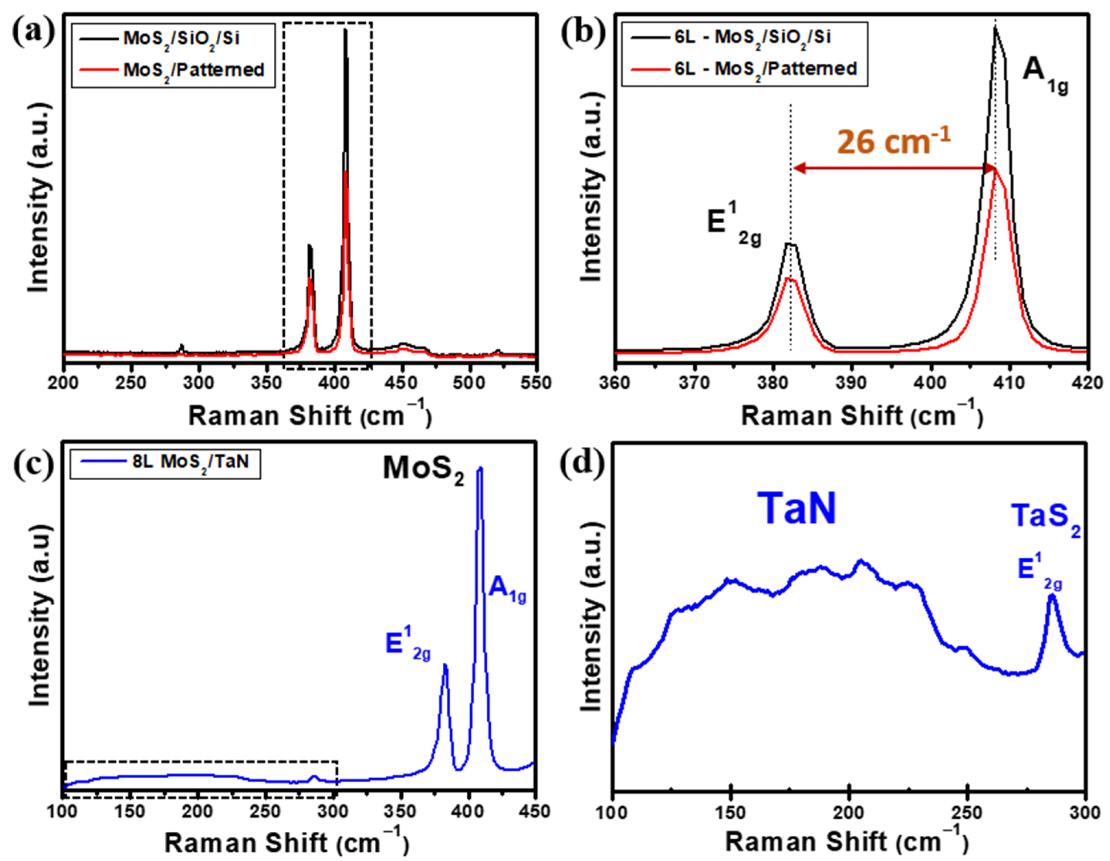
With a similar analytical approach as used for the flat MoS2 nanosheets, we considered micro-Raman spectroscopy to analyse the vertically aligned MoS2 growths. Figure 4a–d shows the Raman spectra of as-grown vertically aligned MoS2 flakes on flat SiO2/Si, pre-patterned SiO2/Si and TaN substrate, respectively. As shown in Figure 4a, the Raman spectrum obtained from MoS2 grown on pre-patterned SiO2/Si substrate (red line) clearly show the main two MoS2 phonon modes E12g and A1g located at 382.9 cm−1 and 409.1 cm−1, respectively. As a further assessment, a dedicated MoS2 growth on flat SiO2/Si substrate targeting similar MoS2 thickness as in the vertical growth case was performed, and its Raman spectrum is shown in Figure 4a (black line) for comparison. The frequency difference of the E12g and A1g Raman modes gives 26 cm−1, as evidenced in Figure 4b, where the phonon mode region corresponding to the dashed box drawn in Figure 4a is plotted. Such value is compatible with the presence of more than 6 MoS2 layers and an overall thickness of >4.2 nm, considering the thickness of a MoS2 monolayer equal to 0.7 nm, as known from the literature [35,36]. Raman spectra of MoS2 on TaN shows MoS2 phonon modes at 381.6 cm−1 for in-plane E12g and 409.8 cm−1 for out-of-plane A1g with a frequency difference of 28.2 cm−1, which corresponds to an eight layer-thick MoS2 on average. In addition, a broad range (100–250 cm−1) of Raman peaks (highlighted by the dashed box) is evident, confirming the presence of preserved TaN after MoS2 growth, as shown in Figure 4c. Figure 4d shows the enlarged Raman region limited by the dashed square in Figure 4c to evidence the presence of a weak Raman peak around 280 cm−1 assigned to the E2g in-plane vibrational mode of 2H-TaS2, which is an indication of the reaction between the interface of TaN and excess sulfur during the CVD growth process. The evidence of 2H-TaS2 is unexpected based on thermochemistry considerations because the chemical reaction from Ta and S to form TaS2 happens at around 900 °C at ambient pressure. Additional factors, such as a supersaturated sulfur atmosphere, out-of-equilibrium conditions, chemistry kinetics or catalytic effects, should be further considered to fully understand the formation of TaS2. As noted above, the weak peaks on the broad region at low Raman shifts are assigned to TaN when stoichiometry modifications occur, either excess of Ta or excess N [32,33].
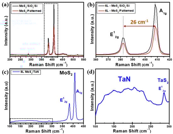
Figure 4.
(a) Raman spectra obtained on vertically aligned MoS2 on pre-patterned (red) and equivalent thick flat (black) SiO2/Si substrate, (b) magnified Raman spectra of panel (a) evidencing E12g (in-plane), A1g (out of plane) phonon modes of MoS2 and their frequency difference. (c) Raman spectrum of vertical aligned MoS2 on TaN substrate and (d) magnification of Raman spectrum in panel (c) in the low Raman shift region (dashed box in (c)), where the presence of co-deposited TaS2 peak is evidenced by its E12g (in-plane) phonon mode.
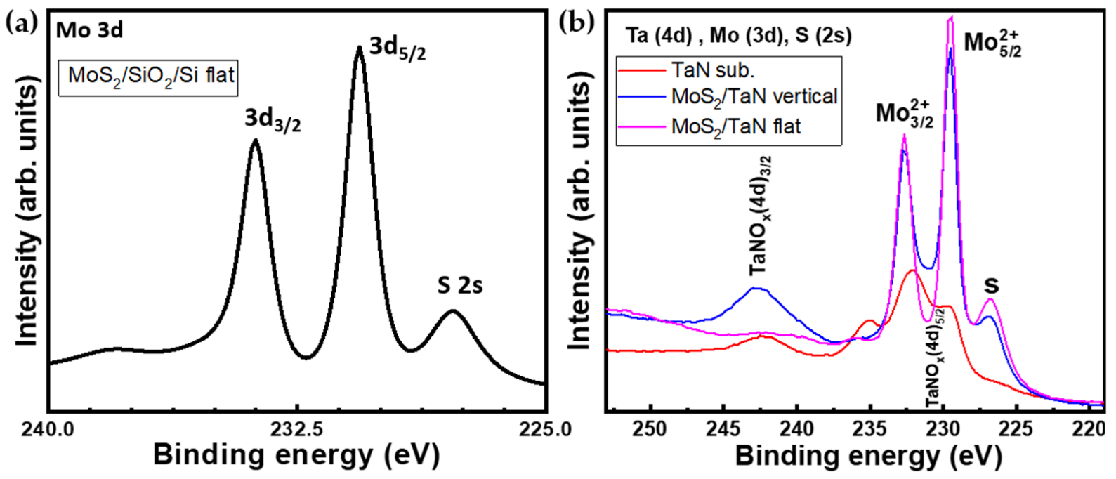
XPS analysis was performed to investigate the elemental composition and chemical bonding of the as-grown MoS2. Figure 5a represents the XPS spectrum of the Mo(3d) and S(2s) spectral region for the CVD grown MoS2 monolayers. The spectral region contains the Mo 3d core-level line with Mo 3d 5/2 at 230.6 eV and Mo 3d 3/2 at 233.7 eV peaks, and the S 2s core-level line peaked at 227.8 eV, all pointing out to Mo-S bonding. The Mo peak positions are indicative of a MoS2 arranged in a majority trigonal prismatic 2H-phase, in agreement with Raman spectroscopy. These results are consistent with previous works on peak positions for MoS2 crystals. This observation constitutes the spectroscopic proof of the presence of Mo and S elements in a MoS2 compound. Figure 5b shows the XPS spectra recorded on vertical and flat aligned MoS2 growth (in blue and magenta, respectively) on TaN substrate together with the bare TaN substrate (red). The spectral windows correspond to Ta-4d, Mo-3d, and S-2s core-level lines. The XPS investigation reveals the presence of Mo, S and TaN in the MoS2 on TaN grown case. The TaN bare substrate (red line) XPS spectrum shows peaks at binding energies around 230.4 eV and 242.5 eV, which are distinctive of the 4d 5/2 and 4d 3/2 states of partially oxidized TaN, such as TaNOx [37]. Such analysis underlies that the pristine TaN substrate is partially oxidized at the surface, possibly due to exposure to the environment. This could be the evidence for the persistence of the TaN layer after the MoS2 growth. XPS of MoS2 on TaN shows prominent peaks at binding energies of around 229.4 eV and 232.6 eV, which are assigned to the doublet of Mo 3d 5/2 and Mo 3d 3/2, respectively. In addition, the sulfur peak (S-2s), located at 226.7 eV, is seen in both flat and vertical MoS2. Interestingly, in the case of flat MoS2 on TaN we do not observe any TaN peak (magenta line) around binding energy 242.5 eV of TaN(Ox), indicating that MoS2 nanosheets are fully covering the TaN film. However, in the vertically-grown MoS2 case (blue line), we clearly found an intense peak of TaNOx at a binding energy of 242.7 eV (4d 3/2) and at 230.6 eV (4d 5/2), where an increase in the valley minimum between Mo related peaks is visible. As reasonable, in the case of vertically aligned MoS2, a partial exposure of TaN substrate persists through the MoS2 domains due to the different growth modes, which compromises the full surface coverage. By comparing the TaN (red) and MoS2 on TaN (blue and magenta), it is also confirmed that TaN keeps preserved during the MoS2 CVD growth process conditions. Thus, the XPS analysis provides further experimental support to show the formation of flat and vertically aligned MoS2 on top of TaN substrate.
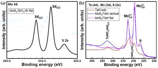
Figure 5.
(a) XPS spectrum shows Mo(3d) and S(2p) core level regions of as-grown MoS2 on SiO2/Si (b) XPS spectra of Ta(4d), Mo(3d) and S(2s) core level regions of as-grown vertical (blue) and flat (magenta) MoS2 on TaN and bare TaN substrate (red).
4. Conclusions
Increasing the control of the deposition process is mandatory for developing desired MoS2 production with fine electrical, optical, and chemical properties. Therefore, we successfully demonstrated a facile and controllable method for the synthesis of large-area MoS2 monolayer to a few layers from MoO3 and S powder precursors using a two-zone furnace AP-CVD system. We showed direct growth of large-area MoS2 on different substrates such as flat and pre-patterned SiO2/Si and TaN, giving an overview of the growth method. This enabled us to display an extensive portfolio of possible configurations spanning from flat MoS2 nanosheets with an atomically controlled thickness on the macro-scale to vertical MoS2 flakes to micro and nano-patterned MoS2 by design, thereby offering a versatile materials background to identify a good MoS2 configuration for a given target application. The configurational variability by changing the precursor positions through furnace movement helped the reaction in favoring the growth orientation. Furthermore, the control of temperature in the MoO3 reaction zone allowed for the growth on the different types of substrates. By optimizing the growth conditions, high-quality horizontally or vertically aligned MoS2 nanosheets were successfully achieved. In a wider context, our results may be of help to stimulate further exploitation in similar growth techniques when applied to 2D materials and their derivatives. We also believe our proposed methodology has the capability for the fabrication of MoS2 based applications, providing a facile synthesizing of TMDs even at the industrial level for a plethora of potential applications.
Supplementary Materials
The following supporting information can be downloaded at: https://www.mdpi.com/article/10.3390/nano12060973/s1, Figure S1. SEM image of MoS2 CVD growth on flat SiO2/Si substrate with no use of PTAS molecules. SEM image shows MoS2 isolated domains small in size, less than 10 μm. A satisfactory surface coverage is not achieved, leaving a relevant region of exposed substrate surface with no MoS2 growth. Figure S2. Picture of SiO2/Si substrate before and after the growth of 1 – 2 layer MoS2 over 1 × 1 cm2 lateral area. Figure S3. SEM images of MoS2 horizontally grown on SiO2/Si substrate, following the edge of the deposited area. The mapped region shows continuous growth over an extended region of several mm. Figure S4. TEM image cross sectional view of monolayer MoS2 on patterned substrate. (a) TEM cross section image shows that MoS2 grows with the basal plane exactly oriented parallel to the SiO2 surface. Here, the MoS2 flake is perfectly following the trenches of the pattern, as represented by the dark black line between the substrate and fixture glue (light gray color). (b) The red region in (a) is shown at higher magnification to ensure the monolayer are following the trench without rupture. Figure S5. SEM image shows cross-sectional view of vertically aligned MoS2 domains on patterned substrate. Figure S6. (a) AFM topographic image of monolayer MoS2 nanosheet on flat SiO2/Si substrate. (b) Height profile of single layer MoS2 along the dashed line in (a) claiming for 0.7 nm step height. AFM analysis evidences the morphology of the CVD grown MoS2 monolayer to be uniformly flat with sharp edges.
Author Contributions
Conceptualization, P.P.T. and A.L.; methodology, P.P.T. and A.L.; writing—original draft preparation, P.P.T.; writing—review and editing, P.P.T., A.L., A.M. and C.M.; supervision, A.L.; project administration, A.L. and A.M.; funding acquisition, A.L. and A.M. All authors have read and agreed to the published version of the manuscript.
Funding
This research was funded by the Italian Government, Ministero dell’Universita e della Ricerca (MUR) under the project PRIN “aSTAR”, grant number 2017RKWTMY. The APC was funded by aSTAR project.
Data Availability Statement
Data can be available upon request from the authors.
Acknowledgments
We acknowledge Mario Alia, CNR-IMM for providing TaN substrates and Erika Kozma, CNR-ISMAC for providing PTAS.
Conflicts of Interest
The authors declare no conflict of interest.
References
- Chhowalla, M.; Shin, H.S.; Eda, G.; Li, L.-J.; Loh, K.P.; Zhang, H. The chemistry of two-dimensional layered transition metal dichalcogenide nanosheets. Nat. Chem. 2013, 5, 263–275. [Google Scholar] [CrossRef] [PubMed]
- Manzeli, S.; Ovchinnikov, D.; Pasquier, D.; Yazyev, O.V.; Kis, A. 2D transition metal dichalcogenides. Nat. Rev. Mater. 2017, 2, 17033. [Google Scholar] [CrossRef]
- Wang, Q.H.; Kalantar-Zadeh, K.; Kis, A.; Coleman, J.N.; Strano, M.S. Electronics and optoelectronics of two-dimensional transition metal dichalcogenides. Nat. Nanotechnol. 2012, 7, 699–712. [Google Scholar] [CrossRef] [PubMed]
- Ryou, J.; Kim, Y.-S.; Santosh, K.C.; Cho, K. Monolayer MoS2 bandgap modulation by dielectric environments and tunable bandgap transistors. Sci. Rep. 2016, 6, 29184. [Google Scholar] [CrossRef] [PubMed]
- Zeng, H.; Cui, X. An optical spectroscopic study on two-dimensional group-VI transition metal dichalcogenides. Chem. Soc. Rev. 2015, 44, 2629–2642. [Google Scholar] [CrossRef]
- Jariwala, D.; Sangwan, V.K.; Lauhon, L.J.; Marks, T.J.; Hersam, M.C. Emerging device applications for semiconducting two-dimensional transition metal dichalcogenides. ACS Nano 2014, 8, 1102–1120. [Google Scholar] [CrossRef] [Green Version]
- Wang, K.; Puretzky, A.A.; Hu, Z.; Srijanto, B.R.; Li, X.; Gupta, N.; Yu, H.; Tian, M.; Mahjouri-Samani, M.; Gao, X.; et al. Strain tolerance of two-dimensional crystal growth on curved surfaces. Sci. Adv. 2019, 5, eaav4028. [Google Scholar] [CrossRef] [Green Version]
- Martella, C.; Mennucci, C.; Lamperti, A.; Cappelluti, E.; de Mongeot, F.B.; Molle, A. Designer shape anisotropy on transition-metal-dichalcogenide nanosheets. Adv. Mater. 2018, 30, 1705615. [Google Scholar] [CrossRef]
- Martella, C.; Ortolani, L.; Cianci, E.; Lamperti, A.; Morandi, V.; Molle, A. Large-area patterning of substrate-conformal MoS2 nano-trenches. Nano Res. 2019, 12, 1851–1854. [Google Scholar] [CrossRef]
- Hus, S.M.; Ge, R.; Chen, P.-A.; Liang, L.; Donnelly, G.E.; Ko, W.; Huang, F.; Chiang, M.-H.; Li, A.-P.; Akinwande, D. Observation of single-defect memristor in an MoS2 atomic sheet. Nat. Nanotechnol. 2020, 16, 58–62. [Google Scholar] [CrossRef] [PubMed]
- Lo, C.-L.; Zhang, K.; Smith, R.S.; Shah, K.; Robinson, J.A.; Chen, Z. Large-area, single-layer molybdenum disulfide synthesized at BEOL compatible temperature as Cu diffusion barrier. IEEE Electron. Device Lett. 2018, 39, 873–876. [Google Scholar] [CrossRef]
- Lo, C.; Catalano, M.; Khosravi, A.; Ge, W.; Ji, Y.; Zemlyanov, D.Y.; Wang, L.; Addou, R.; Liu, Y.; Wallace, R.; et al. Enhancing interconnect reliability and performance by converting tantalum to 2D layered tantalum sulfide at low temperature. Adv. Mater. 2019, 31, e1902397. [Google Scholar] [CrossRef] [PubMed] [Green Version]
- Li, G.; Chen, Z.; Li, Y.; Zhang, D.; Yang, W.; Liu, Y.; Cao, L. Engineering substrate interaction to improve hydrogen evolution catalysis of monolayer MoS2 films beyond Pt. ACS Nano 2020, 14, 1707–1714. [Google Scholar] [CrossRef] [PubMed]
- Voiry, D.; Fullon, R.R.; Yang, J.; de Carvalho Castro e Silva, C.; Kappera, R.; Bozkurt, I.; Kaplan, D.; Lagos, M.J.; Batson, P.E.; Gupta, G.; et al. The role of electronic coupling between substrate and 2D MoS2 nanosheets in electrocatalytic production of hydrogen. Nat. Mater. 2016, 15, 1003–1009. [Google Scholar] [CrossRef]
- Ozden, A.; Ay, F.; Sevik, C.; Perkgöz, N.K. CVD growth of monolayer MoS2: Role of growth zone configuration and precursors ratio. Jpn. J. Appl. Phys. 2017, 56, 06GG05. [Google Scholar] [CrossRef]
- Fan, X.; Xu, P.; Li, Y.C.; Zhou, D.; Sun, Y.; Nguyen, M.A.T.; Terrones, M.; Mallouk, T.E. Controlled exfoliation of MoS2 crystals into trilayer nanosheets. J. Am. Chem. Soc. 2016, 138, 5143–5149. [Google Scholar] [CrossRef]
- Fabbri, F.; Rotunno, E.; Cinquanta, E.; Campi, D.; Bonnini, E.; Kaplan, D.; Lazzarini, L.; Bernasconi, M.; Ferrari, C.; Longo, M.; et al. Novel near-infrared emission from crystal defects in MoS2 multilayer flakes. Nat. Commun. 2016, 7, 13044. [Google Scholar] [CrossRef] [Green Version]
- Tumino, F.; Grazianetti, C.; Martella, C.; Ruggeri, M.; Russo, V.; Li Bassi, A.; Molle, A.; Casari, C.S. Hydrophilic character of single-layer MoS2 grown on Ag(111). J. Phys. Chem. C 2021, 125, 9479–9485. [Google Scholar] [CrossRef]
- Bhatnagar, M.; Gardella, M.; Giordano, M.C.; Chowdhury, D.; Mennucci, C.; Mazzanti, A.; Della Valle, G.; Martella, C.; Tummala, P.; Lamperti, A.; et al. Broadband and tunable light harvesting in nanorippled MoS2 ultrathin films. ACS Appl. Mater. Interfaces 2021, 13, 13508–13516. [Google Scholar] [CrossRef]
- Bhatnagar, M.; Giordano, M.C.; Mennucci, C.; Chowdhury, D.; Mazzanti, A.; Della Valle, G.; Martella, C.; Tummala, P.; Lamperti, A.; Molle, A.; et al. Ultra-broadband photon harvesting in large-area few-layer MoS2 nanostripe gratings. Nanoscale 2020, 12, 24385–24393. [Google Scholar] [CrossRef] [PubMed]
- Fan, X.; Xu, P.; Zhou, D.; Sun, Y.; Li, Y.C.; Nguyen, M.A.T.; Terrones, M.; Mallouk, T.E. Fast and efficient preparation of exfoliated 2H MoS2 nanosheets by sonication-assisted lithium intercalation and infrared laser-induced 1T to 2H phase reversion. Nano Lett. 2015, 15, 5956–5960. [Google Scholar] [CrossRef] [PubMed]
- Zhang, F.; Momeni, K.; Abu AlSaud, M.; Azizi, A.; Hainey, M.F.; Redwing, J.M.; Chen, L.-Q.; Alem, N. Controlled synthesis of 2D transition metal dichalcogenides: From vertical to planar MoS2. 2D Mater. 2017, 4, 25029. [Google Scholar] [CrossRef]
- Miao, C.; Zheng, C.; Liang, O.; Xie, Y.-H. Chemical Vapor Deposition of Graphene. In Physics and Applications of Graphene-Theory; InTech: Rijeka, Croatia, 2011. [Google Scholar]
- Tummala, P.; Lamperti, A.; Alia, M.; Kozma, E.; Nobili, L.G.; Molle, A. Application-oriented growth of a molybdenum disulfide (MoS2) single layer by means of parametrically optimized chemical vapor deposition. Materials 2020, 13, 2786. [Google Scholar] [CrossRef] [PubMed]
- Zhu, D.; Shu, H.; Jiang, F.; Lv, D.; Asokan, V.; Omar, O.; Yuan, J.; Zhang, Z.; Jin, C. Capture the growth kinetics of CVD growth of two-dimensional MoS2. npj 2D Mater. Appl. 2017, 1, 1–8. [Google Scholar] [CrossRef]
- Dos Santos, R.B.; Rivelino, R.; de Brito Mota, F.; Gueorguiev, G.K.; Kakanakova-Georgieva, A. Dopant species with Al–Si and N–Si bonding in the MOCVD of AlN implementing trimethylaluminum, ammonia and silane. J. Phys. D Appl. Phys. 2015, 48, 295104. [Google Scholar] [CrossRef]
- Kakanakova-Georgieva, A.; Gueorguiev, G.K.; Yakimova, R.; Janzen, E. Effect of impurity incorporation on crystallization in AlN sublimation epitaxy. J. Appl. Phys. 2004, 96, 5293–5297. [Google Scholar] [CrossRef]
- Li, H.; Zhang, X.H.; Tang, Z.K. Catalytic growth of large area monolayer molybdenum disulfide film by chemical vapor deposition. Thin Solid Film. 2019, 669, 371–376. [Google Scholar] [CrossRef]
- Momeni, K.; Ji, Y.; Zhang, K.; Robinson, J.A.; Chen, L.-Q. Multiscale framework for simulation-guided growth of 2D materials. Npj 2D Mater. Appl. 2018, 2, 27. [Google Scholar] [CrossRef]
- Navarro-Moratalla, E.; Island, J.O.; Mañas-Valero, S.; Pinilla-Cienfuegos, E.; Castellanos-Gomez, A.; Quereda, J.; Rubio-Bollinger, G.; Chirolli, L.; Silva-Guillén, J.A.; Agraït, N.; et al. Enhanced superconductivity in atomically thin TaS2. Nat. Commun. 2016, 7, 11043. [Google Scholar] [CrossRef] [Green Version]
- Martella, C.; Kozma, E.; Tummala, P.P.; Ricci, S.; Patel, K.A.; Andicsovà-Eckstein, A.; Bertini, F.; Scavia, G.; Sordan, R.; Nobili, L.G.; et al. Changing the electronic polarizability of monolayer MoS2 by perylene-based seeding promoters. Adv. Mater. Interfaces 2020, 7, 2000791. [Google Scholar] [CrossRef]
- Stoehr, M.; Shin, C.-S.; Petrov, I.; Greene, J.E. Raman scattering from epitaxial TaNx(0.94 ≤ x ≤ 1.37) layers grown on MgO(001). J. Appl. Phys. 2007, 101, 123509. [Google Scholar] [CrossRef]
- Huang, J.; Wang, X.; Hogan, N.L.; Wu, S.; Lu, P.; Fan, Z.; Dai, Y.; Zeng, B.; Starko-Bowes, R.; Jian, J.; et al. Nanoscale artificial plasmonic lattice in self-assembled vertically aligned nitride–metal hybrid metamaterials. Adv. Sci. 2018, 5, 1800416. [Google Scholar] [CrossRef] [PubMed]
- Splendiani, A.; Sun, L.; Zhang, Y.; Li, T.; Kim, J.; Chim, C.-Y.; Galli, G.; Wang, F. Emerging photoluminescence in monolayer MoS2. Nano Lett. 2010, 10, 1271–1275. [Google Scholar] [CrossRef] [PubMed]
- Chakraborty, B.; Matte, H.S.S.R.; Sood, A.K.; Rao, C.N.R. Layer-dependent resonant Raman scattering of a few layer MoS2. J. Raman Spectrosc. 2013, 44, 92–96. [Google Scholar] [CrossRef]
- Lee, Y.-H.; Yu, L.; Wang, H.; Fang, W.; Ling, X.; Shi, Y.; Lin, C.-T.; Huang, J.-K.; Chang, M.-T.; Chang, C.-S.; et al. Synthesis and transfer of single-layer transition metal disulfides on diverse surfaces. Nano Lett. 2013, 13, 1852–1857. [Google Scholar] [CrossRef] [PubMed]
- Husain, S.; Akansel, S.; Kumar, A.; Svedlindh, P.; Chaudhary, S. Growth of Co2FeAl Heusler alloy thin films on Si(100) having very small Gilbert damping by Ion beam sputtering. Sci. Rep. 2016, 6, 28692. [Google Scholar] [CrossRef] [PubMed] [Green Version]

Publisher’s Note: MDPI stays neutral with regard to jurisdictional claims in published maps and institutional affiliations. |
© 2022 by the authors. Licensee MDPI, Basel, Switzerland. This article is an open access article distributed under the terms and conditions of the Creative Commons Attribution (CC BY) license (https://creativecommons.org/licenses/by/4.0/).