
Control of Ni/β-Ga2O3 Vertical Schottky Diode Output Parameters at Forward Bias by Insertion of a Graphene Layer


Abstract
:1. Introduction
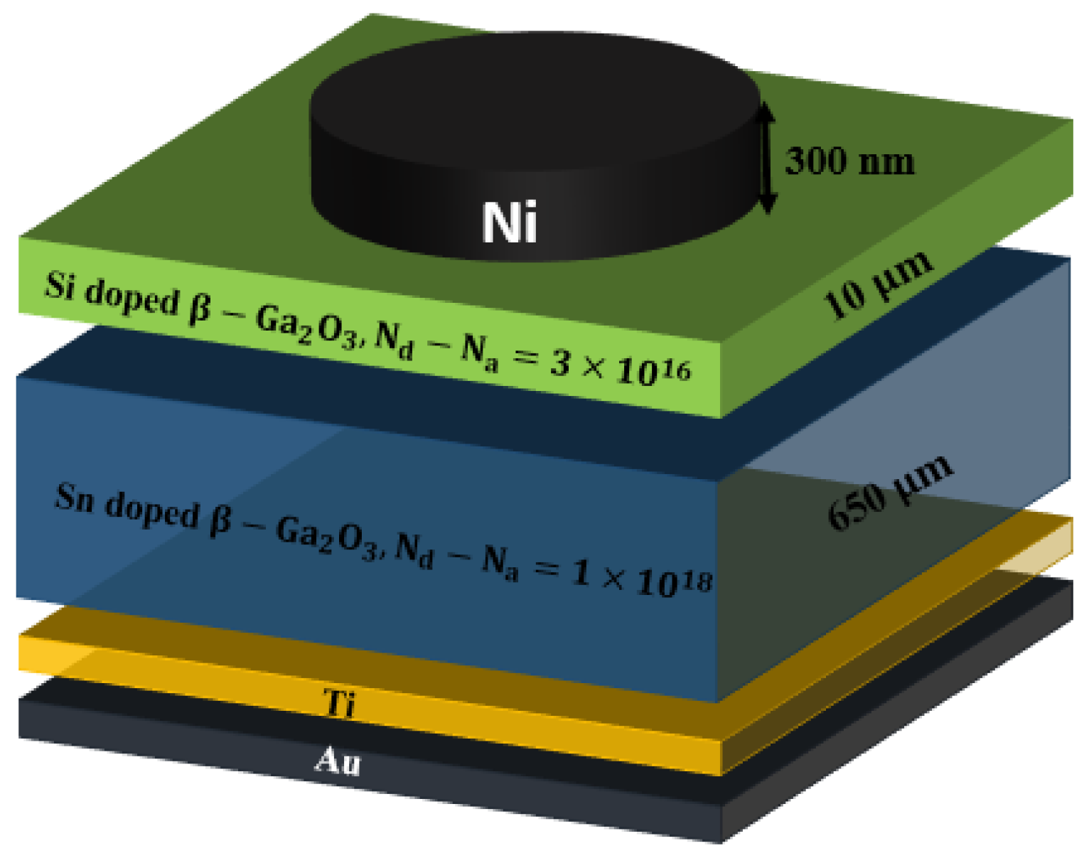
2. Experimental
3. Simulation Methodology
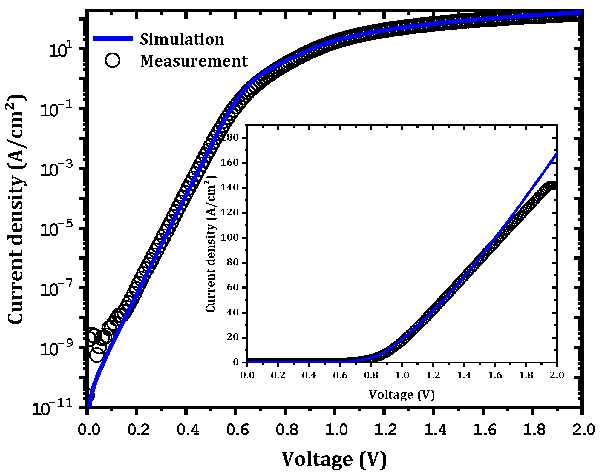
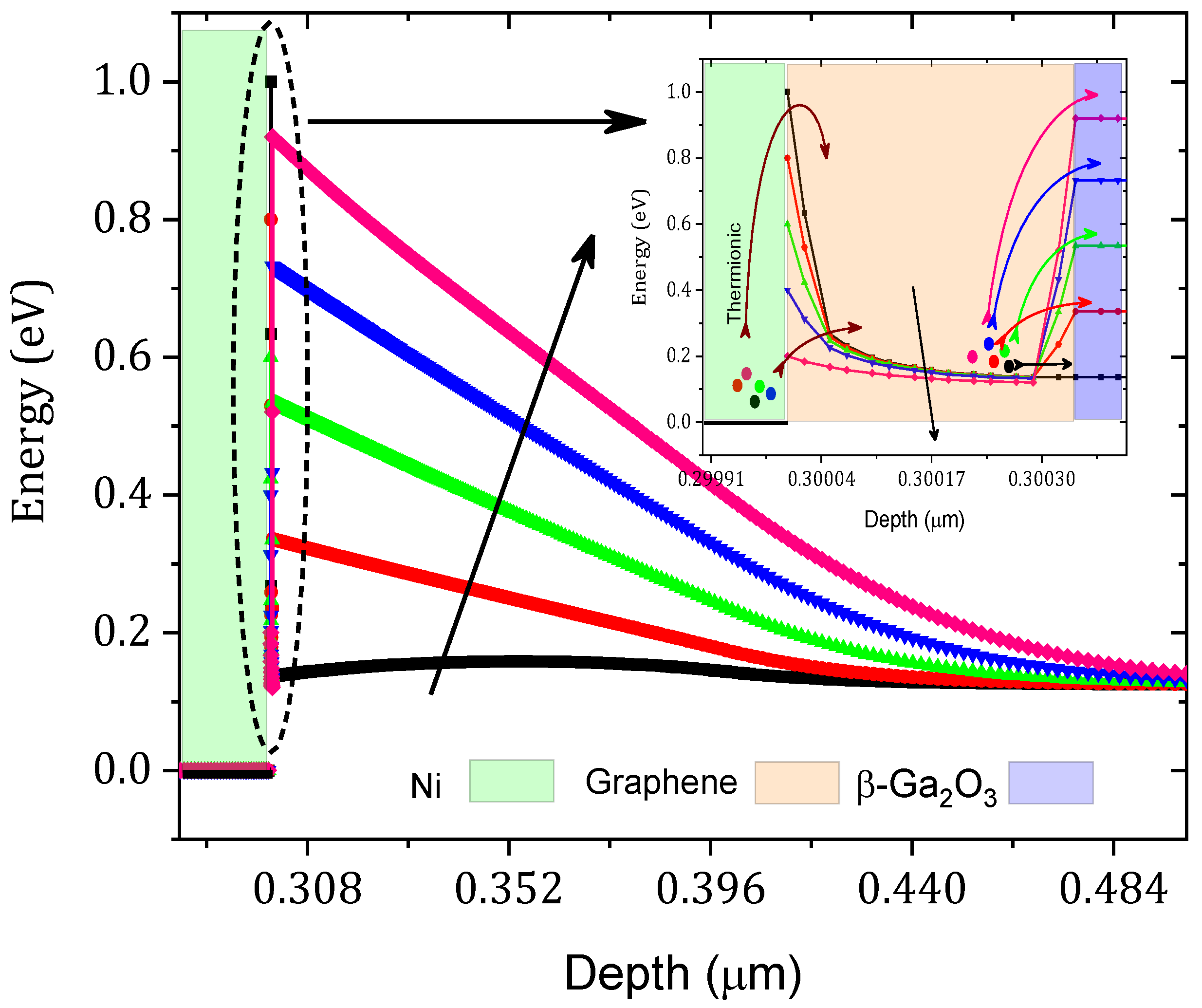
4. Results
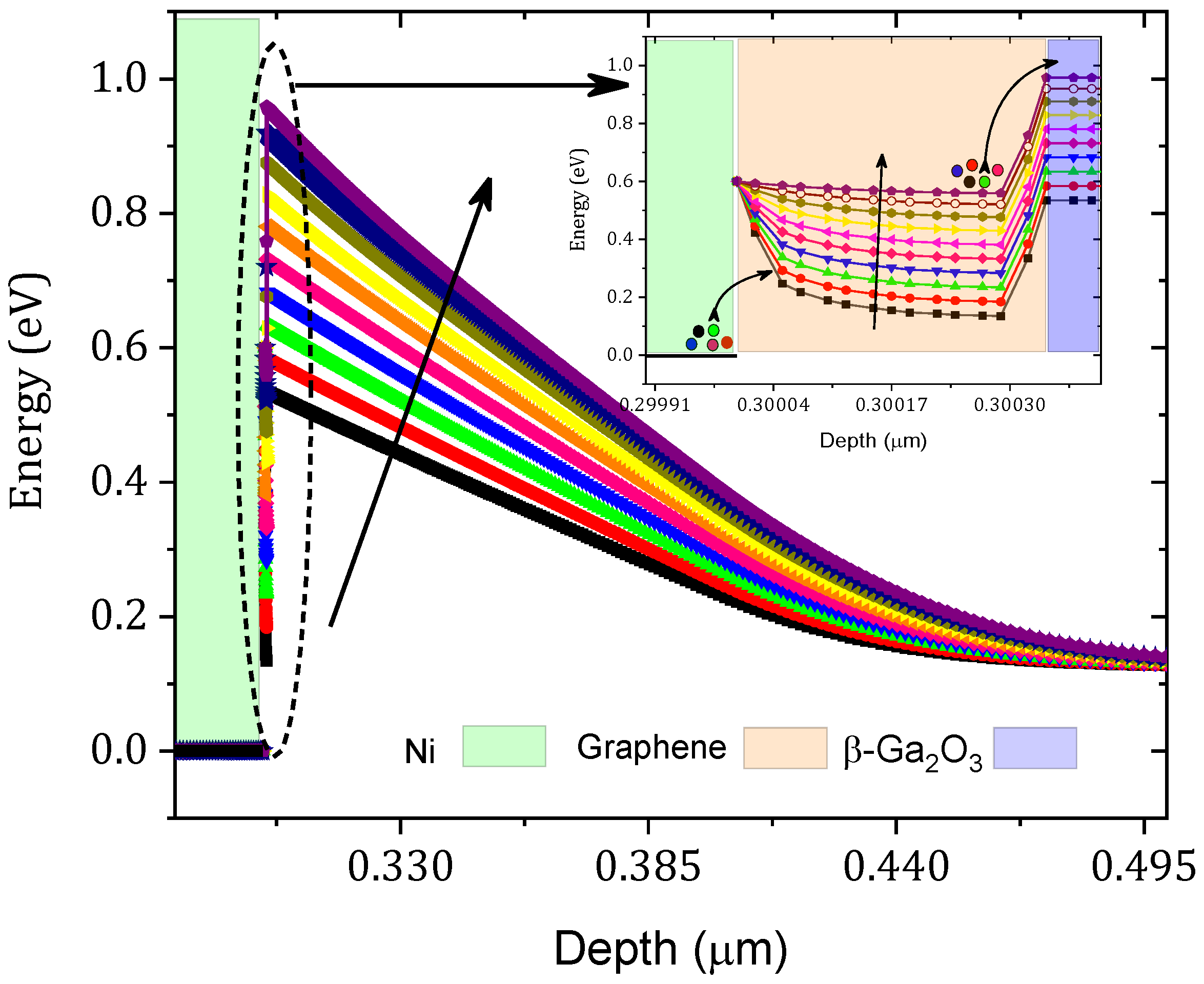
4.1. Effect of Insertion of a Graphene Layer
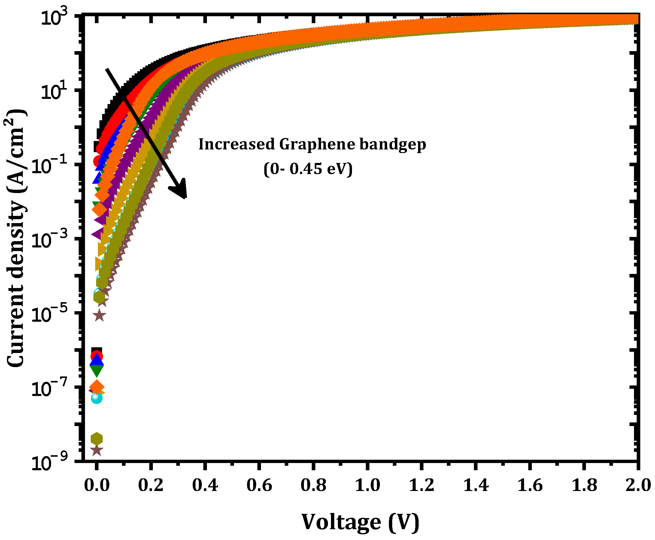
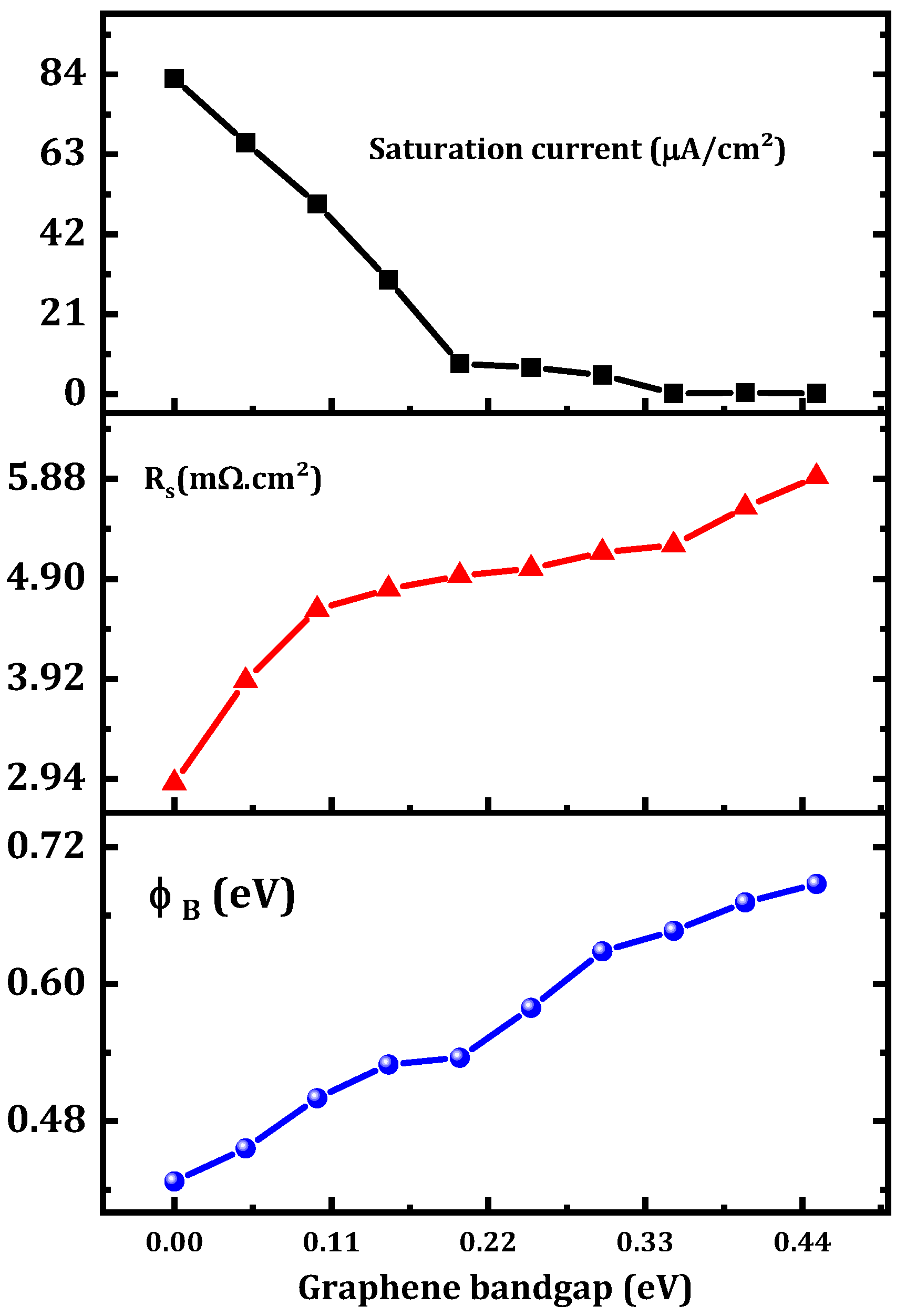
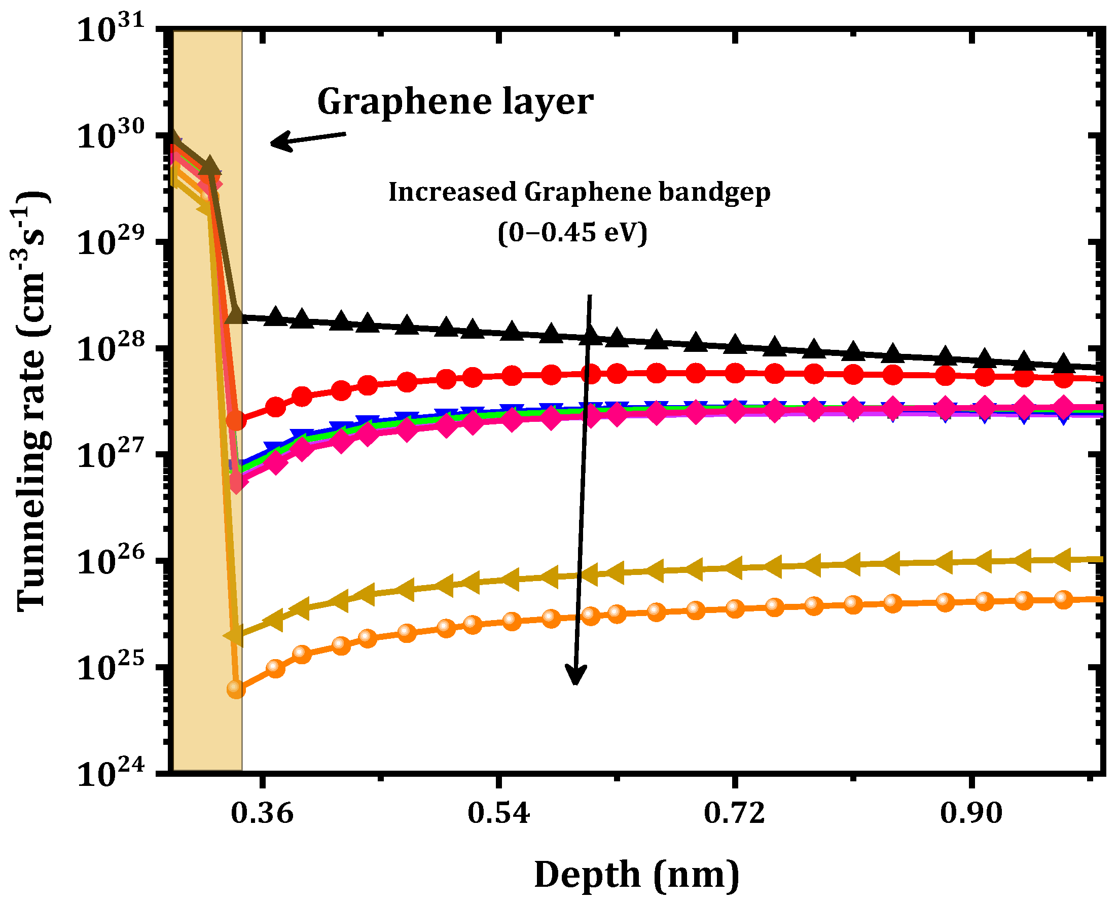
4.2. Graphene Bandgap Effect
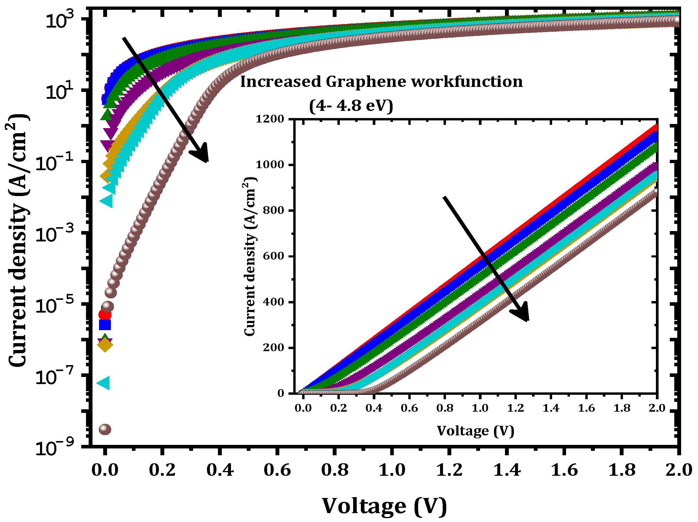
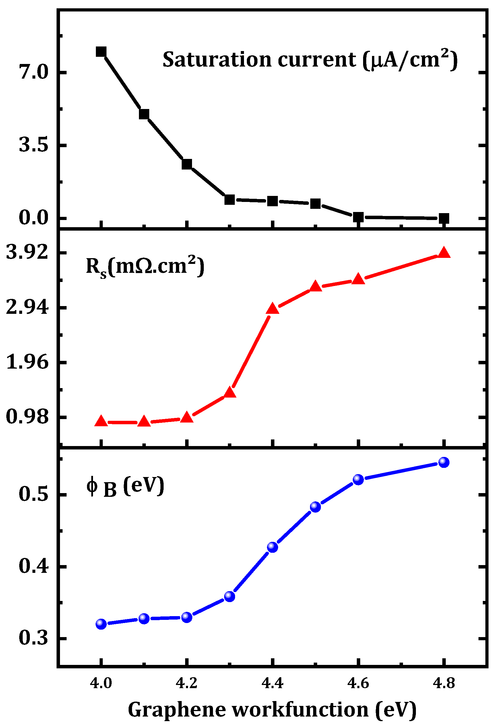
4.3. Graphene Workfunction Effect
5. Conclusions
Author Contributions
Funding
Conflicts of Interest
References
- Xue, H.; He, Q.; Jian, G.; Long, S.; Pang, T.; Liu, M. An Overview of the Ultrawide Bandgap Ga2O3 Semiconductor-Based Schottky Barrier Diode for Power Electronics Application. Nanoscale Res. Lett. 2018, 13, 290. [Google Scholar] [CrossRef] [PubMed] [Green Version]
- Labed, M.; Sengouga, N.; Labed, M.; Meftah, A.; Kyoung, S.; Kim, H.; Rim, Y.S. Modeling a Ni/β-Ga2O3 Schottky barrier diode deposited by confined magnetic-field-based sputtering. J. Phys. D Appl. Phys. 2021, 54, 115102. [Google Scholar] [CrossRef]
- Polyakov, A.Y.; Lee, I.-H.; Smirnov, N.B.; Yakimov, E.B.; Shchemerov, I.V.; Chernykh, A.V.; Kochkova, A.I.; Vasilev, A.A.; Carey, P.H.; Ren, F.; et al. Defects at the surface of β-Ga2O3 produced by Ar plasma exposure. APL Mater. 2019, 7, 061102. [Google Scholar] [CrossRef] [Green Version]
- Galazka, Z. β-Ga2O3 for wide-bandgap electronics and optoelectronics. Semicond. Sci. Technol. 2018, 33, 113001. [Google Scholar] [CrossRef]
- Kyrtsos, A.; Matsubara, M.; Bellotti, E. On the feasibility of p-type Ga2O3. Appl. Phys. Lett. 2018, 112, 032108. [Google Scholar] [CrossRef]
- Chikoidze, E.; Sartel, C.; Mohamed, H.; Madaci, I.; Tchelidze, T.; Modreanu, M.; Vales-Castro, P.; Rubio, C.; Arnold, C.; Sallet, V.; et al. Enhancing the intrinsic p-type conductivity of the ultra-wide bandgap Ga2O3 semiconductor. J. Mater. Chem. C 2019, 7, 10231–10239. [Google Scholar] [CrossRef]
- Labed, M.; Sengouga, N.; Meftah, A.; Labed, M.; Kyoung, S.; Kim, H.; Rim, Y.S. Leakage Current Modelling and Optimization of β-Ga2O3 Schottky Barrier Diode with Ni Contact under High Reverse Voltage. ECS J. Solid State Sci. Technol. 2020, 9, 125001. [Google Scholar] [CrossRef]
- Kokubun, Y.; Kubo, S.; Nakagomi, S. All-oxide p–n heterojunction diodes comprising p-type NiO and n-type β-Ga2O3. Appl. Phys. Express 2016, 9, 91101. [Google Scholar] [CrossRef]
- Gong, H.; Zhou, F.; Xu, W.; Yu, X.; Xu, Y.; Yang, Y.; Ren, F.; Gu, S.; Zheng, Y.; Zhang, R.; et al. 1.37 kV/12 A NiO/β-Ga2O3 Heterojunction Diode With Nanosecond Reverse Recovery and Rugged Surge-Current Capability. IEEE Trans. Power Electron. 2021, 36, 12213–12217. [Google Scholar] [CrossRef]
- Watahiki, T.; Yuda, Y.; Furukawa, A.; Yamamuka, M.; Takiguchi, Y.; Miyajima, S. Heterojunction p-Cu2O/n-Ga2O3 diode with high breakdown voltage. Appl. Phys. Lett. 2017, 111, 222104. [Google Scholar] [CrossRef]
- Jian, G.; He, Q.; Mu, W.; Fu, B.; Dong, H.; Qin, Y.; Zhang, Y.; Xue, H.; Long, S.; Jia, Z.; et al. Characterization of the inhomogeneous barrier distribution in a Pt/(100) β-Ga2O3 Schottky diode via its temperature-dependent electrical properties. AIP Adv. 2018, 8, 015316. [Google Scholar] [CrossRef] [Green Version]
- Pearton, S.J.; Ren, F.; Tadjer, M.; Kim, J. Perspective: Ga2O3 for ultra-high power rectifiers and MOSFETS. J. Appl. Phys. 2018, 124, 220901. [Google Scholar] [CrossRef] [Green Version]
- Thomas, S.R.; Adamopoulos, G.; Lin, Y.-H.; Faber, H.; Sygellou, L.; Stratakis, E.; Pliatsikas, N.; Patsalas, P.A.; Anthopoulos, T.D. High electron mobility thin-film transistors based on Ga2O3 grown by atmospheric ultrasonic spray pyrolysis at low temperatures. Appl. Phys. Lett. 2014, 105, 092105. [Google Scholar] [CrossRef]
- Grillo, A.; Barrat, J.; Galazka, Z.; Passacantando, M.; Giubileo, F.; Iemmo, L.; Luongo, G.; Urban, F.; Dubourdieu, C.; Di Bartolomeo, A. High field-emission current density from β-Ga2O3 nanopillars. Appl. Phys. Lett. 2019, 114, 193101. [Google Scholar] [CrossRef]
- Harada, T.; Tsukazaki, A. Control of Schottky barrier height in metal/β-Ga2O3 junctions by insertion of PdCoO2 layers. APL Mater. 2020, 8, 41109. [Google Scholar] [CrossRef] [Green Version]
- Tung, R.T. The physics and chemistry of the Schottky barrier height. Appl. Phys. Rev. 2014, 1, 11304. [Google Scholar] [CrossRef] [Green Version]
- Farzana, E.; Zhang, Z.; Paul, P.K.; Arehart, A.R.; Ringel, S.A. Influence of metal choice on (010) β-Ga2O3 Schottky diode properties. Appl. Phys. Lett. 2017, 110, 202102. [Google Scholar] [CrossRef]
- Yao, Y.; Gangireddy, R.; Kim, J.; Das, K.K.; Davis, R.F.; Porter, L.M. Electrical behavior of β-Ga2O3 Schottky diodes with different Schottky metals. J. Vac. Sci. Technol. B Nanotechnol. Microelectron. Mater. Process. Meas. Phenom. 2017, 35, 03D113. [Google Scholar] [CrossRef]
- Bhattacharyya, A.; Ranga, P.; Saleh, M.; Roy, S.; Scarpulla, M.A.; Lynn, K.G.; Krishnamoorthy, S. Schottky Barrier Height Engineering in β-Ga2O3 Using SiO2 Interlayer Dielectric. IEEE J. Electron Devices Soc. 2020, 8, 286–294. [Google Scholar] [CrossRef]
- Kim, H.; Kyoung, S.; Kang, T.; Kwon, J.Y.; Kim, K.H.; Rim, Y.S. Effective surface diffusion of nickel on single crystal β-Ga2O3 for Schottky barrier modulation and high thermal stability. J. Mater. Chem. C 2019, 7, 10953–10960. [Google Scholar] [CrossRef]
- Labed, M.; Sengouga, N.; Meftah, A.; Meftah, A.; Rim, Y.S. Study on the improvement of the open-circuit voltage of NiOx/Si heterojunction solar cell. Opt. Mater. 2021, 120, 111453. [Google Scholar] [CrossRef]
- Courtin, J.; Le Gall, S.; Chrétien, P.; Moréac, A.; Delhaye, G.; Lépine, B.; Tricot, S.; Turban, P.; Schieffer, P.; Le Breton, J.-C. A low Schottky barrier height and transport mechanism in gold–graphene–silicon (001) heterojunctions. Nanoscale Adv. 2019, 1, 3372–3378. [Google Scholar] [CrossRef] [Green Version]
- Zhu, X.; Lei, S.; Tsai, S.-H.; Zhang, X.; Liu, J.; Yin, G.; Tang, M.; Torres, C.M.; Navabi, A.; Jin, Z.; et al. A Study of Vertical Transport through Graphene toward Control of Quantum Tunneling. Nano Lett. 2018, 18, 682–688. [Google Scholar] [CrossRef] [PubMed]
- Tiras, E.; Ardali, S.; Tiras, T.; Arslan, E.; Cakmakyapan, S.; Kazar, O.; Hassan, J.; Janzén, E.; Ozbay, E. Effective mass of electron in monolayer graphene: Electron-phonon interaction. J. Appl. Phys. 2013, 113, 43708. [Google Scholar] [CrossRef]
- Dadashbeik, M.; Fathi, D.; Eskandari, M. Design and simulation of perovskite solar cells based on graphene and TiO2/graphene nanocomposite as electron transport layer. Sol. Energy 2020, 207, 917–924. [Google Scholar] [CrossRef]
- Labed, M.; Sengouga, N.; Labed, M.; Meftah, A.; Kyoung, S.; Kim, H.; Rim, Y.S. Modeling and analyzing temperature-dependent parameters of Ni/β-Ga2O3 Schottky barrier diode deposited by confined magnetic field-based sputtering. Semicond. Sci. Technol. 2021, 36, 35020. [Google Scholar] [CrossRef]
- Yuan, H.; Su, J.; Guo, R.; Tian, K.; Lin, Z.; Zhang, J.; Chang, J.; Hao, Y. Contact barriers modulation of graphene/β-Ga2O3 interface for high-performance Ga2O3 devices. Appl. Surf. Sci. 2020, 527, 146740. [Google Scholar] [CrossRef]
- Zhong, H.; Xu, K.; Liu, Z.; Xu, G.; Shi, L.; Fan, Y.; Wang, J.; Ren, G.; Yang, H. Charge transport mechanisms of graphene/semiconductor Schottky barriers: A theoretical and experimental study. J. Appl. Phys. 2014, 115, 13701. [Google Scholar] [CrossRef]
- Inaba, M.; Suzuki, K.; Shibuya, M.; Lee, C.-Y.; Masuda, Y.; Tomatsu, N.; Norimatsu, W.; Hiraiwa, A.; Kusunoki, M.; Kawarada, H. Very low Schottky barrier height at carbon nanotube and silicon carbide interface. Appl. Phys. Lett. 2015, 106, 123501. [Google Scholar] [CrossRef]
- Takahashi, T.; Sugawara, K.; Noguchi, E.; Sato, T.; Takahashi, T. Band-gap tuning of monolayer graphene by oxygen adsorption. Carbon N. Y. 2014, 73, 141–145. [Google Scholar] [CrossRef]
- Hussain, A.; Ullah, S.; Farhan, M.A. Fine tuning the band-gap of graphene by atomic and molecular doping: A density functional theory study. RSC Adv. 2016, 6, 55990–56003. [Google Scholar] [CrossRef]
- Xu, X.; Liu, C.; Sun, Z.; Cao, T.; Zhang, Z.; Wang, E.; Liu, Z.; Liu, K. Interfacial engineering in graphene bandgap. Chem. Soc. Rev. 2018, 47, 3059–3099. [Google Scholar] [CrossRef] [PubMed]
- Hibino, H.; Kageshima, H.; Kotsugi, M.; Maeda, F.; Guo, F.-Z.; Watanabe, Y. Dependence of electronic properties of epitaxial few-layer graphene on the number of layers investigated by photoelectron emission microscopy. Phys. Rev. B 2009, 79, 125437. [Google Scholar] [CrossRef]
- Naghdi, S.; Sanchez-Arriaga, G.; Rhee, K.Y. Tuning the work function of graphene toward application as anode and cathode. J. Alloys Compd. 2019, 805, 1117–1134. [Google Scholar] [CrossRef] [Green Version]


| Parameters | Sn: β-Ga2O3 | Si: β-Ga2O3 | Graphene |
|---|---|---|---|
| Bandgap (eV) | 4.8 | 4.8 | 0–0.45 |
| Affinity (eV) | 4 | 4 | 4–4.8 |
| 10 | 10 | 9000 | |
| 172 | 300 | 9000 | |
| Relative permittivity | 12.6 | 11 | 6.9 |
| / | |||
| Thickness (µm) | 650 | 10 | 0.34 × 10⁻³ |
Publisher’s Note: MDPI stays neutral with regard to jurisdictional claims in published maps and institutional affiliations. |
© 2022 by the authors. Licensee MDPI, Basel, Switzerland. This article is an open access article distributed under the terms and conditions of the Creative Commons Attribution (CC BY) license (https://creativecommons.org/licenses/by/4.0/).
Share and Cite
Labed, M.; Sengouga, N.; Rim, Y.S. Control of Ni/β-Ga2O3 Vertical Schottky Diode Output Parameters at Forward Bias by Insertion of a Graphene Layer. Nanomaterials 2022, 12, 827. https://doi.org/10.3390/nano12050827
Labed M, Sengouga N, Rim YS. Control of Ni/β-Ga2O3 Vertical Schottky Diode Output Parameters at Forward Bias by Insertion of a Graphene Layer. Nanomaterials. 2022; 12(5):827. https://doi.org/10.3390/nano12050827
Chicago/Turabian StyleLabed, Madani, Nouredine Sengouga, and You Seung Rim. 2022. "Control of Ni/β-Ga2O3 Vertical Schottky Diode Output Parameters at Forward Bias by Insertion of a Graphene Layer" Nanomaterials 12, no. 5: 827. https://doi.org/10.3390/nano12050827
APA StyleLabed, M., Sengouga, N., & Rim, Y. S. (2022). Control of Ni/β-Ga2O3 Vertical Schottky Diode Output Parameters at Forward Bias by Insertion of a Graphene Layer. Nanomaterials, 12(5), 827. https://doi.org/10.3390/nano12050827