Article

Dimension-Dependent Phenomenological Model of Excitonic Electric Dipole in InGaAs Quantum Dots

1
Department of Condensed Matter Physics, Faculty of Science, Masaryk University, Kotlářská 267/2, 61137 Brno, Czech Republic
2
Huygens-Kamerlingh Onnes Laboratory, Leiden University, P.O. Box 9504, 2300 RA Leiden, The Netherlands
3
Czech Metrology Institute, Okružní 31, 63800 Brno, Czech Republic
*
Author to whom correspondence should be addressed.
Nanomaterials 2022, 12(4), 719; https://doi.org/10.3390/nano12040719
Submission received: 24 January 2022 / Revised: 13 February 2022 / Accepted: 18 February 2022 / Published: 21 February 2022

Abstract

:
Permanent electric dipole is a key property for effective control of semiconductor quantum-dot-based sources of quantum light. For theoretical prediction of that, complex geometry-dependent quantum simulations are necessary. Here, we use k · p simulations of exciton transition in InGaAs quantum dots to derive a simple geometry-dependent analytical model of dipole. Our model, discussed here, enables reasonably good estimation of the electric dipole, caused in quantum dot by the elastic strain, including an externally induced one. Due to its apparent simplicity, not necessitating elaborate and time-consuming simulations, it might after experimental verification serve as a preferred choice for experimentalists enabling them to make quick estimates of built-in and induced electric dipole in quantum dots.

1. Introduction

Due to their discrete energy levels with the molecular-like character [1] and strong quantum confinement of electrons and holes in all dimensions [2], semiconductor quantum dots (QDs) serve as an excellent solid-state platform for a number of appealing applications. Among others, they may be used as gain material for semiconductor lasers [3,4] or as building blocks of nonvolatile universal memory, so-called QD-Flash [5,6]. Due to near unity quantum efficiency and external-field tuneability, QD optical transitions are often used as sources of quantum light [7,8] in advanced quantum communication and computation schemes [9,10]. This application demands well-defined transitions energies and control of QDs’ interaction with the charge environment.
Permanent electric dipole (p) is one of the key properties of semiconductor quantum dots connecting their electronic structure with optical activity. Since it directly relates to the separation of electron and hole wavefunction [11,12], it can be used for identification of the type of QD spatial confinement. More importantly, the dipole plays significant role in fine-tuning of QDs’ emission energies through in-plane applied electriec field via quantum Stark effect [13,14]. Such control of emission energies is used in cavity quantum electrodynamics for tuning QD emission into resonance with optical cavity [8,15], or for control of photon indistinguishability from remote quantum emitters [16,17].
Even though theoretical predictions of the electric dipole of QDs with realistic shape currently exist, they are typically based on complex single-particle quantum simulations requiring a definition of the full heterostructure, strain energy minimalization in that, and quantification of the related strain and piezoelectricity-induced changes of the confinement potentials [2]. In principle, such calculation can be done with atomistic precision within empirical pseudopotential [18,19] or tight-binding models [2,20], but since that approach is computational-heavy, it is typically used for QDs with a rather small volume. To account for effects at macroscopic dimensions, tight-binding models are typically replaced with computationally lighter approximate semiempirical methods based on macroscopic properties of the heterostructure, such as k · p simulations [21,22]. Because performing such advanced simulations requires years of experience with complex software tools [23], hands-on approximations of geometry-dependent electric dipole for QDs are practical but nonexistent to date. Therefore, in this study, we extend model from our recent work [24] on QD-geometry-induced changes of electric dipole and discuss a phenomenological model of the electric dipole motivated by analytical estimation of p of 1D quantum well [25,26] and found by systematic analysis of a set of k · p simulations.

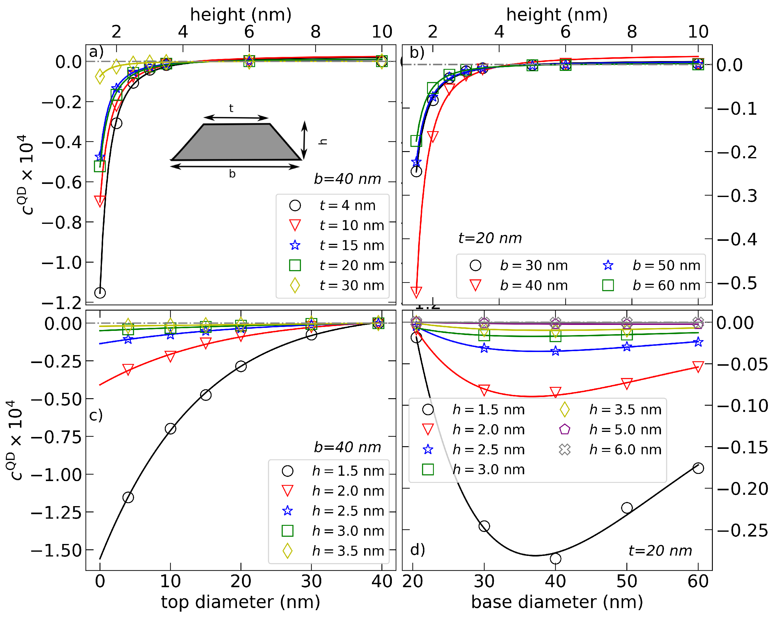
2. Modeling of Electric Dipole

In our previous work [24], we showed that the electrical polarization P and the corresponding built-in dipole moment in stress-tuned In x Ga 1 x As/GaAs QDs [27] are mainly influenced by one of the second-order terms in the expansion of P into strain ( η ), the dominant term is denoted by the coefficient B 124 . Based on that observation, an approximate formula to reproduce p as a function of applied shear in-plane stress σ x y appl was derived
p / e A QD ( σ x y appl + σ x y pre + σ x y QD ) ,
where σ x y pre represents off-diagonal component of the (symmetric) in-plane prestress induced in the heterostructure by bonding on the piezoelectric actuators for external stress tuning, σ x y QD is the in-plane component of hydrostatic stress in QD, and e denotes the elementary charge. That relation allows splitting changes of p into contributions driven by the stress-tuning and terms purely related to build-in QD dipole effected only by QD lattice relaxation-induced hydrostatic stress. Since the scaling factor A QD can be written as [24]
A QD = C QD B 124 η H QD e G ,
we can further separate QD geometry, represented by geometry-dependent scaling factor C QD , from hydrostatic strain effects. In Equation (2), B 124 represents the second-order term in the expansion of P ; G and η H QD are the shear modulus and the hydrostatic strain in QD, respectively. Values of parameters B 124 and G for a specific QD’s material composition x are estimated by linear interpolation of parameters listed in Table 1.
Since the parameter C QD reflects the quantum confinement effect on the quasiparticle position in QD, quantum simulations are needed for its quantification. In this work, we extract the parameter C QD from simulations of p calculated for a truncated cone shape In x Ga 1 x As QD by eight-band k · p approximation. In our simulations, we keep In-Ga alloy distribution constant at value showing good agreement in emission energy, fine-structures splitting of QD exciton, and p between theory and experiment ( x = 0.45 ) [24] and vary only QD spatial dimensions, i.e., QD’s top (t) and bottom (b) diameter, and height (h).
The full calculation flow of simulations discussed in this work was as follows. First, the geometry of the QD structure was defined on a rectangular grid including the spatially dependent material constituents. Thereafter, the strain field in and around QD was found by minimizing the strain energy, followed by calculation of the effect of resulting strain on the confinement potential was then calculated using the Bir-Pikus Hamiltonian with positionally dependent material parameters listed in the supplementary materials of [24]. In the next step, the self-consistent solution of single-particle Schrödinger and Poisson equations including the effect of piezoelectric fields up to second order in η were calculated by Nextnano3 simulation suite [23]. The obtained single-particle states within the envelope function method based on an eight-band k · p approximation are then used for accounting for multiparticle interactions, including direct and exchange Coulomb interaction [31,32,33]. Restricting ourselves only to bright exciton transition, we use the multiparticle corrected electronic states for p calculation, i.e., the distance between electron- and hole-wavefunctions center of mass. Assuming that the geometrical dependency of C QD for any QD shape will for laterally large dots converge to the dependency p h 4 derived for infinitely large 1D potential well of thickness h [25,26], we can quantify the dipole correction for the lateral quantum confinement by further analysis of c QD as
C QD = c QD h 4 .
By careful cross-analysis of simulated sets of p for varying t, b, and h presented in the panels of Figure 1, we find that c QD can be approximated by
c QD = A ( b t ) exp B | b t | h + D .
Now, we analyze the fitted parameters A, B, and D, shown in Figure 2. Parameter A in Figure 2a) is found to be independent of the QD lateral dimensions, while it clearly retains a residue dependency on QD height. This dependency is stronger for smaller QDs and exponentially disappears for taller dots. Contrary, parameter B in Figure 2b) shows strong dependency only on lateral dimensions, where it increases proportionally to the dot top diameter B 1 / t and decreases with its base diameter as B 1 / b . Finally, c QD for laterally big QDs converges to the parameter D, represented in Figure 2c). Even though we initially assumed D to be geometry-independent, it still shows a dependency for small QDs. That dependency, together with high statistical error from our fits, could be related to an artefact of rough simulation grid in k · p calculations, where the electron wavefunction with the tendency to be located at the top of the dot would need a finer grid for better convergence.
The presented model merges together into one simple analytical expression two methods used for estimation of QD electric dipole. On the one hand, it is an extension of the already existing, explicitly geometry-dependent model of p derived for 1D well [25,26], used widely also in QD research, on lateral confinement. On the other hand, our model is developed from complex k · p simulations of realistic QDs, where the electron and hole eigenstates of QD, and thus also p, are corrected for piezoelectricity, stress, and many-body effects. Note that due to the form of Equation (4), our model also correctly describes the sign of p in QD with reverted vertical orientation.
The model relies only on the validation of the approximation from Equation (1), derived under assumptions: (i) the QD has type-I confinement, (ii) it consists from piezoelectric material with dominant second-order term B 124 , and (iii) the hydrostatic strain around QD is mostly driven by the material mismatch between the dot and the substrate η H QD . Because the model is proportional not only to QD geometry but also to material parameters, it can be, therefore, expected to be applicable also for other III-V QD systems [14,34,35,36,37] with type-I confinement where the electric dipole is aligned only along the dot growth direction.

3. Conclusions

In conclusion, we show a phenomenological analytical model describing the excitonic electric dipole of In 0.45 Ga 0.55 As QDs with geometry-dependent parameters quantifying quantum confinement effect. The presented simple model of electric dipole agrees with dipole simulation done with complex eight-band k · p approximation, which recently fully described single-quantum dot experiments [24]. The presented model, being a 3D confinement extension of model derived for 1D well [25,26], needs to be further tested on a combination of morphology and single QD spectroscopy data set. Thereafter, due to its strong dependency on individual spatial properties of studied QDs, it can serve as a rough but straightforward estimate of QD’s spatial dimensions directly from spectroscopic measurements without necessity of additional information taken from, e.g., STM measurements [38].

Author Contributions

Conceptualization, P.S. and P.K.; methodology, P.S. and P.K.; software, P.S. and P.K.; validation, P.S. and P.K.; formal analysis, P.S.; investigation, P.S.; resources, P.S.; data curation, P.S. and P.K.; writing—original draft preparation, P.S. and P.K.; writing—review and editing, P.K.; visualization, P.S.; supervision, P.K.; project administration, P.K.; funding acquisition, P.K. All authors have read and agreed to the published version of the manuscript.

Funding

P.S. acknowledges funding from the EU Horizon 2020 programme (GA 862035 QLUSTER). P.S. and P.K. were financed by the project CUSPIDOR that received funding from the QuantERA ERA-NET Cofund in Quantum Technologies implemented within the European Union’s Horizon 2020 program and from the MEYS of the Czech Republic under grant agreement ID: 731473. The work reported in this paper also was partially funded by projects 20IND05 QADeT, 20FUN05 SEQUME, and 17FUN06 Siqust that received funding from the EMPIR program cofinanced by the Participating States and from the European Union’s Horizon 2020 research and innovation program.

Institutional Review Board Statement

Not applicable.

Informed Consent Statement

Not applicable.

Data Availability Statement

The data that support the findings of this study are available upon reasonable request from the authors.

Conflicts of Interest

The funders had no role in the design of the study; in the collection, analyses, or interpretation of data; in the writing of the manuscript, or in the decision to publish the results.

References

  1. Kastner, M.A. Artificial Atoms. Phys. Today 1993, 46, 24–31. [Google Scholar] [CrossRef]
  2. Mittelstädt, A.; Schliwa, A.; Klenovský, P. Modeling electronic and optical properties of III–V quantum dots—Selected recent developments. Light. Sci. Appl. 2022, 11, 1–14. [Google Scholar] [CrossRef] [PubMed]
  3. Heinrichsdorff, F.; Mao, M.H.; Kirstaedter, N.; Krost, A.; Bimberg, D.; Kosogov, A.O.; Werner, P. Room-temperature continuous-wave lasing from stacked InAs/GaAs quantum dots grown by metalorganic chemical vapor deposition. Appl. Phys. Lett. 1997, 71, 22–24. [Google Scholar] [CrossRef]
  4. Klenovský, P.; Brehm, M.; Křápek, V.; Lausecker, E.; Munzar, D.; Hackl, F.; Steiner, H.; Fromherz, T.; Bauer, G.; Humlíček, J. Excitation intensity dependence of photoluminescence spectra of SiGe quantum dots grown on prepatterned Si substrates: Evidence for biexcitonic transition. Phys. Rev. B 2012, 86. [Google Scholar] [CrossRef] [Green Version]
  5. Sala, E.M. Growth and Characterization of Antimony-Based Quantum Dots in GaP Matrix For Nanomemories. Ph.D. Thesis, Technische Universität Berlin, Berlin, Germany, 2018. [Google Scholar] [CrossRef]
  6. Sala, E.M.; Arikan, I.F.; Bonato, L.; Bertram, F.; Veit, P.; Christen, J.; Strittmatter, A.; Bimberg, D. MOVPE-Growth of InGaSb/AlP/GaP(001) Quantum Dots for Nanoscale Memory Applications. Phys. Status Solidi B 2018, 1800182. [Google Scholar] [CrossRef]
  7. Ding, X.; He, Y.; Duan, Z.C.; Gregersen, N.; Chen, M.C.; Unsleber, S.; Maier, S.; Schneider, C.; Kamp, M.; Höfling, S.; et al. On-Demand Single Photons with High Extraction Efficiency and Near-Unity Indistinguishability from a Resonantly Driven Quantum Dot in a Micropillar. Phys. Rev. Lett. 2016, 116, 6. [Google Scholar] [CrossRef] [Green Version]
  8. Snijders, H.; Frey, J.A.; Norman, J.; Post, V.P.; Gossard, A.C.; Bowers, J.E.; Van Exter, M.P.; Löffler, W.; Bouwmeester, D. Fiber-Coupled Cavity-QED Source of Identical Single Photons. Phys. Rev. Appl. 2018, 9, 31002. [Google Scholar] [CrossRef] [Green Version]
  9. Snijders, H.J.; Frey, J.A.; Norman, J.; Flayac, H.; Savona, V.; Gossard, A.C.; Bowers, J.E.; Van Exter, M.P.; Bouwmeester, D.; Löffler, W. Observation of the Unconventional Photon Blockade. Phys. Rev. Lett. 2018, 121, 43601. [Google Scholar] [CrossRef] [Green Version]
  10. Kok, P.; Munro, W.J.; Nemoto, K.; Ralph, T.C.; Dowling, J.P.; Milburn, G.J. Linear optical quantum computing with photonic qubits. Rev. Mod. Phys. 2007, 79, 135–174. [Google Scholar] [CrossRef] [Green Version]
  11. Klenovský, P.; Hemzal, D.; Steindl, P.; Zíková, M.; Křápek, V.; Humlíček, J. Polarization anisotropy of the emission from type-II quantum dots. Phys. Rev. B 2015, 92, 241302. [Google Scholar] [CrossRef] [Green Version]
  12. Murphy-Armando, F.; Brehm, M.; Steindl, P.; Lusk, M.T.; Fromherz, T.; Schwarz, K.; Blaha, P. Light emission from direct band gap germanium containing split-interstitial defects. Phys. Rev. B 2021, 103, 85310. [Google Scholar] [CrossRef]
  13. Bennett, A.J.; Patel, R.B.; Skiba-Szymanska, J.; Nicoll, C.A.; Farrer, I.; Ritchie, D.A.; Shields, A.J. Giant Stark effect in the emission of single semiconductor quantum dots. Appl. Phys. Lett. 2010, 97, 1–4. [Google Scholar] [CrossRef] [Green Version]
  14. Huang, H.; Csontosová, D.; Manna, S.; Huo, Y.; Trotta, R.; Rastelli, A.; Klenovský, P. Electric field induced tuning of electronic correlation in weakly confining quantum dots. Phys. Rev. B 2021, 104, 165401. [Google Scholar] [CrossRef]
  15. Steindl, P.; Snijders, H.; Westra, G.; Hissink, E.; Iakovlev, K.; Polla, S.; Frey, J.A.; Norman, J.; Gossard, A.C.; Bowers, J.E.; et al. Artificial Coherent States of Light by Multiphoton Interference in a Single-Photon Stream. Phys. Rev. Lett. 2021, 126, 143601. [Google Scholar] [CrossRef] [PubMed]
  16. Reindl, M.; Jöns, K.D.; Huber, D.; Schimpf, C.; Huo, Y.; Zwiller, V.; Rastelli, A.; Trotta, R. Phonon-Assisted Two-Photon Interference from Remote Quantum Emitters. Nano Lett. 2017, 17, 4090–4095. [Google Scholar] [CrossRef]
  17. Weber, J.H.; Kambs, B.; Kettler, J.; Kern, S.; Maisch, J.; Vural, H.; Jetter, M.; Portalupi, S.L.; Becher, C.; Michler, P. Two-photon interference in the telecom C-band after frequency conversion of photons from remote quantum emitters. Nat. Nanotechnol. 2019, 14, 23–26. [Google Scholar] [CrossRef] [Green Version]
  18. Williamson, A.J.; Wang, L.W.; Zunger, A. Theoretical interpretation of the experimental electronic structure of lens-shaped self-assembled InAs/GaAs quantum dots. Phys. Rev. B 2000, 62, 12963–12977. [Google Scholar] [CrossRef] [Green Version]
  19. Bester, G.; Zunger, A. Cylindrically shaped zinc-blende semiconductor quantum dots do not have cylindrical symmetry: Atomistic symmetry, atomic relaxation, and piezoelectric effects. Phys. Rev. B 2005, 71, 045318. [Google Scholar] [CrossRef] [Green Version]
  20. Slater, J.C.; Koster, G.F. Simplified LCAO Method for the Periodic Potential Problem. Phys. Rev. 1954, 94, 1498. [Google Scholar] [CrossRef]
  21. Schliwa, A.; Winkelnkemper, M.; Bimberg, D. Impact of size, shape, and composition on piezoelectric effects and electronic properties of In(Ga)AsGaAs quantum dots. Phys. Rev. B 2007, 76, 205324. [Google Scholar] [CrossRef] [Green Version]
  22. Schliwa, A.; Winkelnkemper, M.; Bimberg, D. Few-particle energies versus geometry and composition of InxGa1-xAs/GaAs self-organized quantum dots. Phys. Rev. B 2009, 79, 075443. [Google Scholar] [CrossRef]
  23. Birner, S.; Zibold, T.; Andlauer, T.; Kubis, T.; Sabathil, M.; Trellakis, A.; Vogl, P. Nextnano: General purpose 3-D simulations. IEEE Trans. El. Dev. 2007, 54, 2137. [Google Scholar] [CrossRef]
  24. Klenovský, P.; Steindl, P.; Aberl, J.; Zallo, E.; Trotta, R.; Rastelli, A.; Fromherz, T. Effect of second-order piezoelectricity on the excitonic structure of stress-tuned In(Ga)As/GaAs quantum dots. Phys. Rev. B 2018, 97, 1–6. [Google Scholar] [CrossRef] [Green Version]
  25. Silver, M.; Greene, P.D.; Adams, A.R. Tailoring the heavy-hole and light-hole quantum-confined Stark effect using multistrain-stepped quantum wells. Appl. Phys. Lett. 1995, 67, 2904. [Google Scholar] [CrossRef]
  26. Barker, J.A.; O’Reilly, E.P. Theoretical analysis of electron-hole alignment in InAs-GaAs quantum dots. Phys. Rev. B 2000, 61, 13840–13851. [Google Scholar] [CrossRef] [Green Version]
  27. Aberl, J.; Klenovský, P.; Wildmann, J.S.; Martín-Sánchez, J.; Fromherz, T.; Zallo, E.; Humlíček, J.; Rastelli, A.; Trotta, R. Inversion of the exciton built-in dipole moment in In(Ga)As quantum dots via nonlinear piezoelectric effect. Phys. Rev. B 2017, 96, 045414. [Google Scholar] [CrossRef] [Green Version]
  28. Beya-Wakata, A.; Prodhomme, P.Y.; Bester, G. First- and second-order piezoelectricity in III-V semiconductors. Phys. Rev. B 2011, 84, 195207. [Google Scholar] [CrossRef]
  29. Burenkov, Y.A.; Davydov, S.Y.; Nikanorov, S.P. Elastic properties of Indium-Arsenide. Sov. Phys. Solid State 1975, 17, 2183–2186. [Google Scholar]
  30. Burenkov, Y.A.; Burdukov, Y.M.; Davydov, S.Y.; Nikanorov, S.P. Temperature-dependence of Gallium-Arsenide elastic-constants. Sov. Phys. Solid State 1973, 156, 1757–1761. [Google Scholar]
  31. Klenovský, P.; Steindl, P.; Geffroy, D. Excitonic structure and pumping power dependent emission blue-shift of type-II quantum dots. Sci. Rep. 2017, 7, 1–10. [Google Scholar] [CrossRef] [Green Version]
  32. Klenovský, P.; Schliwa, A.; Bimberg, D. Electronic states of (InGa)(AsSb)/GaAs/GaP quantum dots. Phys. Rev. B 2019, 100, 115424. [Google Scholar] [CrossRef] [Green Version]
  33. Csontosová, D.; Klenovský, P. Theory of magneto-optical properties of neutral and charged excitons in GaAs/AlGaAs quantum dots. Phys. Rev. B 2020, 102, 125412. [Google Scholar] [CrossRef]
  34. Steindl, P.; Sala, E.M.; Alén, B.; Marrón, D.F.; Bimberg, D.; Klenovský, P. Optical response of (InGa)(AsSb)/GaAs quantum dots embedded in a GaP matrix. Phys. Rev. B 2019, 195407. [Google Scholar] [CrossRef]
  35. Steindl, P.; Sala, E.M.; Alén, B.; Bimberg, D.; Klenovský, P. On the importance of antimony for temporal evolution of emission from self-assembled (InGa)(AsSb)/GaAs quantum dots on GaP(001). New J. Phys. 2021, 23, 103029. [Google Scholar] [CrossRef]
  36. Rautert, J.; Shamirzaev, T.S.; Nekrasov, S.V.; Yakovlev, D.R.; Klenovský, P.; Kusrayev, Y.G.; Bayer, M. Optical orientation and alignment of excitons in direct and indirect band gap (In,Al)As/AlAs quantum dots with type-I band alignment. Phys. Rev. B 2019, 99, 195411. [Google Scholar] [CrossRef] [Green Version]
  37. Sala, E.M.; Godsland, M.; Trapalis, A.; Heffernan, J. Effect of Cap Thickness on InAs/InP Quantum Dots Grown by Droplet Epitaxy in Metal–Organic Vapor Phase Epitaxy. Phys. Status Solidi Rapid Res. Lett. 2021, 15, 2100283. [Google Scholar] [CrossRef]
  38. Gajjela, R.S.R.; Hendriks, A.L.; Douglas, J.O.; Sala, E.M.; Steindl, P.; Bagot, P.A.J.; Moody, M.P.; Bimberg, D.; Koenraad, P.M.; Klenovský, P. Structural and compositional analysis of (InGa) (AsSb)/GaAs/ GaP Stranski—Krastanov quantum dots. Light Sci. Appl. 2021, 10, 125. [Google Scholar] [CrossRef]
Figure 1. Comparison of c QD (multiplied by factor 10 4 ) extracted from k · p simulations (symbols) with the model Equation (4) (curves) for QD with fixed b = 40 nm and varying t and h [panels (a) and (c)], and QD with fixed t = 20 nm and varying b and h [in (b,d)], respectively.
Nanomaterials 12 00719 g001
Figure 2. Fitting parameters A [panel (a)], B [panel (b)], and D [panel (c)] from analysis of c QD given in Figure 1 by Equation (4). Parameters A and D are multiplied by factors 10 6 and 10 4 , respectively, for the sake of better visibility. Parameters extracted from fits of the data dependency of c QD on base (top) are plotted here as a function of height with black (yellow) triangles. Similarly, parameters extracted from height dependency are plotted as a function of base (top) diameter in blue (red).
Nanomaterials 12 00719 g002
Table 1. Parameter values used in k · p calculation and in Equation (2).
B 124 ( C / m 2 ) [28]G (GPa)
InAs 4.1 19.00 [29]
GaAs 3.8 32.85 [30]
Publisher’s Note: MDPI stays neutral with regard to jurisdictional claims in published maps and institutional affiliations.

