Article

Tin Oxide (SnO2) Nanoparticles: Facile Fabrication, Characterization, and Application in UV Photodetectors

1
Nantong Normal College, Nantong 226010, China
2
School of Chemistry and Chemical Engineering, Nantong University, Nantong 226019, China
*
Authors to whom correspondence should be addressed.
Nanomaterials 2022, 12(4), 632; https://doi.org/10.3390/nano12040632
Submission received: 15 December 2021 / Revised: 27 January 2022 / Accepted: 8 February 2022 / Published: 14 February 2022
(This article belongs to the Special Issue Xene-Related Nanostructures for Versatile Applications)

Abstract

:
Tin oxide (SnO2) nanomaterials are of great interest in many fields such as catalytic, electrochemical, and biomedical applications, due to their low cost, suitable stability characteristics, high photosensitivity, etc. In this contribution, SnO2 NPs were facilely fabricated by calcination of tin (II) oxalate in air, followed by a liquid-phase exfoliation (LPE) method. Size-selected SnO2 NPs were easily obtained using a liquid cascade centrifugation (LCC) technique. The as-obtained SnO2 NPs displayed strong absorption in the UV region (~300 nm) and exhibited narrower absorption characteristics with a decrease in NP size. The as-fabricated SnO2 NPs were, for the first time, directly deposited onto a poly(ethylene terephthalate) (PET) film with a regular Ag lattice to fabricate a flexible working electrode for a photoelectrochemical (PEC)-type photodetector. The results demonstrated that the SnO2-NP-based electrode showed the strongest photoresponse signal in an alkaline electrolyte compared with those in neutral and acidic electrolytes. The maximum photocurrent density reached 14.0 μA cm−2, significantly outperforming black phosphorus nanosheets and black phosphorus analogue nanomaterials such as tin (II) sulfide nanosheets and tellurene. The as-fabricated SnO2 NPs with relatively larger size had better self-powered photoresponse performance. In addition, the as-fabricated SnO2-NP-based PEC photodetector exhibited strong cycling stability for on/off switching behavior under ambient conditions. It is anticipated that SnO2 nanostructures, as building blocks, can offer diverse availabilities for high-performance self-powered optoelectronic devices to realize a carbon-neutral or carbon-free environment.

1. Introduction

A variety of strategies have been proposed over the last three decades to address critical global issues such as energy shortages and the impacts of a carbon-free environment [1,2,3,4,5]. Optoelectronic devices based on semiconducting materials have shown promising potential for utilizing abundant solar energy [6,7,8,9]. To date, a great deal of research has focused on the rational fabrication of high-performance semiconducting nanomaterials such as two-dimensional (2D) black phosphorus (BP) and its analogues [10,11], 2D tellurene [12], 0D or 2D selenium (Se) nanomaterials [13,14], etc., for their excellent optoelectronic device performances. For example, in 2017, Zhang et al. [11] successfully fabricated large-sized BP nanosheets (NSs) using a facile liquid-phase exfoliation (LPE) method, and these were employed as electrode materials to fabricate self-powered photodetectors displaying comparable photoresponse activity and environmental robustness under light illumination. In 2018, Ye et al. [15] successfully synthesized large-area, high-quality 2D tellurene NSs, with tunable thickness from a monolayer to tens of nanometers, and with lateral sizes of up to 100 µm, by a hydrothermal method. These exhibited high on/off ratios (106), environmentally excellent stability, and carrier mobilities of about 700 cm2 V−1 s−1. Furthermore, in 2019, our group [6] rationally synthesized telluride–selenium (Te–Se) roll-to-roll nanotubes with different Se contents by epitaxial growth of Se on precursor Te nanotubes. These not only demonstrated a significantly improved capacity for self-powered photodetection but also remarkably enhanced the photocurrent density and stability in various aqueous electrolytes such as HCl, NaCl, and KOH solutions. However, the environmental instability of nanostructures (e.g., BP NSs and Se NSs) upon exposure to air, and the complex, time-consuming, and high-cost synthetic process make it difficult for them to satisfy the growing requirements of modern devices. Therefore, the exploitation of high-quality, cost-effective, and stable self-powered nanostructures is of great value for the performance optimization of optoelectronic devices.
It is well known that a standard photodetector should meet the “5S” requirement: high sensitivity, high signal-to-noise ratio, high spectral selectivity, high speed, and high stability [16,17]. Self-powered UV photodetectors play a vital role in many commercial and scientific applications including flame sensing, optical communication, satellite launching, biological and chemical analysis, and astronomical studies [18,19,20]. SnO2, a IV–VI semiconductor, is used as a UV detection material due to a variety of merits such as its suitable bandgap (3.6–4.0 eV) [7,21], high chemical stability, high electron mobility [22], etc. These characteristics make it suitable for many intriguing applications such as in batteries [23,24], sensors [25,26], catalysis [27,28], solar cells [22,29], water purification [7,30,31], and biomedical applications [32,33]. Moreover, the bandgap energy of SnO2 has great potential for bridging the bandgap space between BP (0.3–2.0 eV) [1,11], and hexagonal boron nitride (5.0–6.0 eV) [34]. These features of SnO2 make it a promising semiconducting material for practical application in self-powered UV photodetectors under ambient conditions, and it holds great promise in the field of renewable energy and renewable energy consumption for the achievement of carbon neutrality targets.
In this contribution, SnO2 nanostructures were facilely synthesized by calcination of tin (II) oxalate at 700 °C in air, and a combination of liquid-phase exfoliation (LPE) and liquid cascade centrifugation (LCC) was carried out to prepare size-selected SnO2 NPs. The as-prepared SnO2 NPs had an average diameter of 92 nm, 78 nm, and 56 nm as the centrifugation speed in the LCC process was increased. All the SnO2 NPs displayed strong absorptionn in the UV region (~300 nm) with relatively narrower absorption characteristics with a decrease in NP size. The as-fabricated SnO2 NPs were, for the first time, directly deposited onto a poly(ethylene terephthalate) (PET) film with a regular Ag lattice, to fabricate a flexible electrode for a photoelectrochemical (PEC)-type photodetector. The photoresponse results for this PEC-type photodetector demonstrated that it not only showed the strongest photoresponse signal in an alkaline electrolyte compared with those in neutral and acidic electrolytes, with maximum photocurrent density of 14.0 μA cm−2, but also displayed excellent self-powered photoresponse performance, as well as high stability in an alkaline electrolyte. Due to the facile fabrication, tunable UV absorption, excellent self-powered response and high environmental stability, it is expected that the present work can provide fundamental guidance on self-powered PEC photodetectors based on SnO2 nanostructures and inspire more research interest in next-generation devices, to achieve carbon neutrality targets.

2. Experimental Section

2.1. Materials

Tin (II) oxalate powder (99.9%), isopropyl alcohol (IPA, 99.9%), dimethyl formamide (DMF, 99.9%), poly(vinylidene fluoride) (PVDF, Mn = 71,000 g mol−1), and dimethyl formamide (DMF, 99.9%)were purchased from Sigma-Aldrich, Shanghai, China and used as received. PET film with a regular Ag lattice was purchased from IVTech-Jiangsu Co., Ltd., Nantong, Jiangsu, China. Hydrochloric acid (HCl, 38%), potassium chloride (KCl, 99.9%), and potassium hydroxide (KOH, 99.9%) were purchased from Alfa Aesar, Haverhill, MA, USA and used as received. Double-distilled deionized water was used for the preparation of the aqueous electrolyte.

2.2. Fabrication of SnO2 NPs

SnO2 nanostructures were facilely synthesized by calcination of tin (II) oxalate powder in air at 600 °C and 700 °C for a predetermined time (4 h and 8 h). Then, the as-obtained SnO2 nanostructures were dispersed into IPA solvent with a concentration of 12 mg mL−1 for sonication overnight at room temperature. An LCC technique was employed to collect different sizes of SnO2 NPs. For convenience, the SnO2 NPs collected at the centrifugation speed ranges of 2000–3000 rps, 5000–6000 rps, and 9000–10,000 rps were abbreviated as SnO2 NPs-1, SnO2 NPs-2, and SnO2 NPs-3. If not specified, SnO2 NPs denotes that they were obtained at a centrifugation speed range of 2–10 k.

2.3. Characterization

X-ray diffraction (XRD) patterns were obtained using a D8 Discover 25 X-ray diffractometer (Bruker) with a Cu K (k = 1.54056 Å) radiation source at room temperature collected from 5° to 85°. The morphology and dimension of the SnO2 nanostructures were determined by scanning electron microscopy (SEM, JSM-6701F, JEOL) and transmission electron microscopy (TEM, FEI F30, 300 kV) at an acceleration voltage of 5.0 kV with sample sputtering applied before analysis. The atomic arrangement of the as-fabricated SnO2 NPs was determined by high-resolution TEM (HRTEM). The SnO2 NPs sample was loaded onto ultrathin carbon-coated holey copper support films with 300-mesh copper grids for TEM measurements. UV–Vis absorbance spectrometry (Cary 60, Agilent, Santa Clara, CA, USA) with a spectral range of 200–1100 nm was performed to record UV–Vis–NIR absorption spectra of all the fabricated SnO2 NPs at room temperature. A typical photoresponse behavior was studied using a PEC measurement system [35,36]. The three-electrode system consisted of a working electrode (SnO2 NPs deposited on a clean PET film with a regular Ag lattice, photoanode), a counter electrode (platinum wire, photocathode), and a reference electrode (a saturated calomel electrode), together with aqueous electrolytes (0.05 M HCl, 0.05 M KCl, and 0.05 M, 0.10 M, and 0.50 M KOH). Amperometric current–time (It) curves were recorded at bias voltages of −0.4 V, −0.2 V, and 0 V under laser irradiation with different power densities (Table S1). Electrochemical impedance spectra (EIS) were collected at an amplitude of 0.005 V in the frequency range from 1 to 105 Hz.

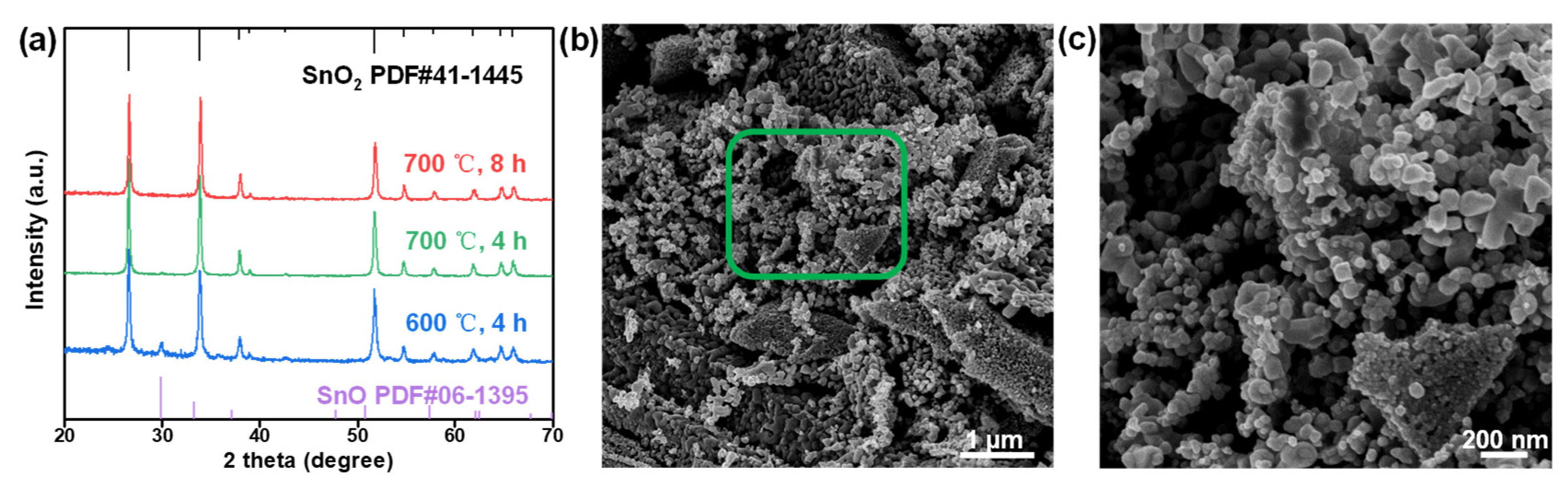
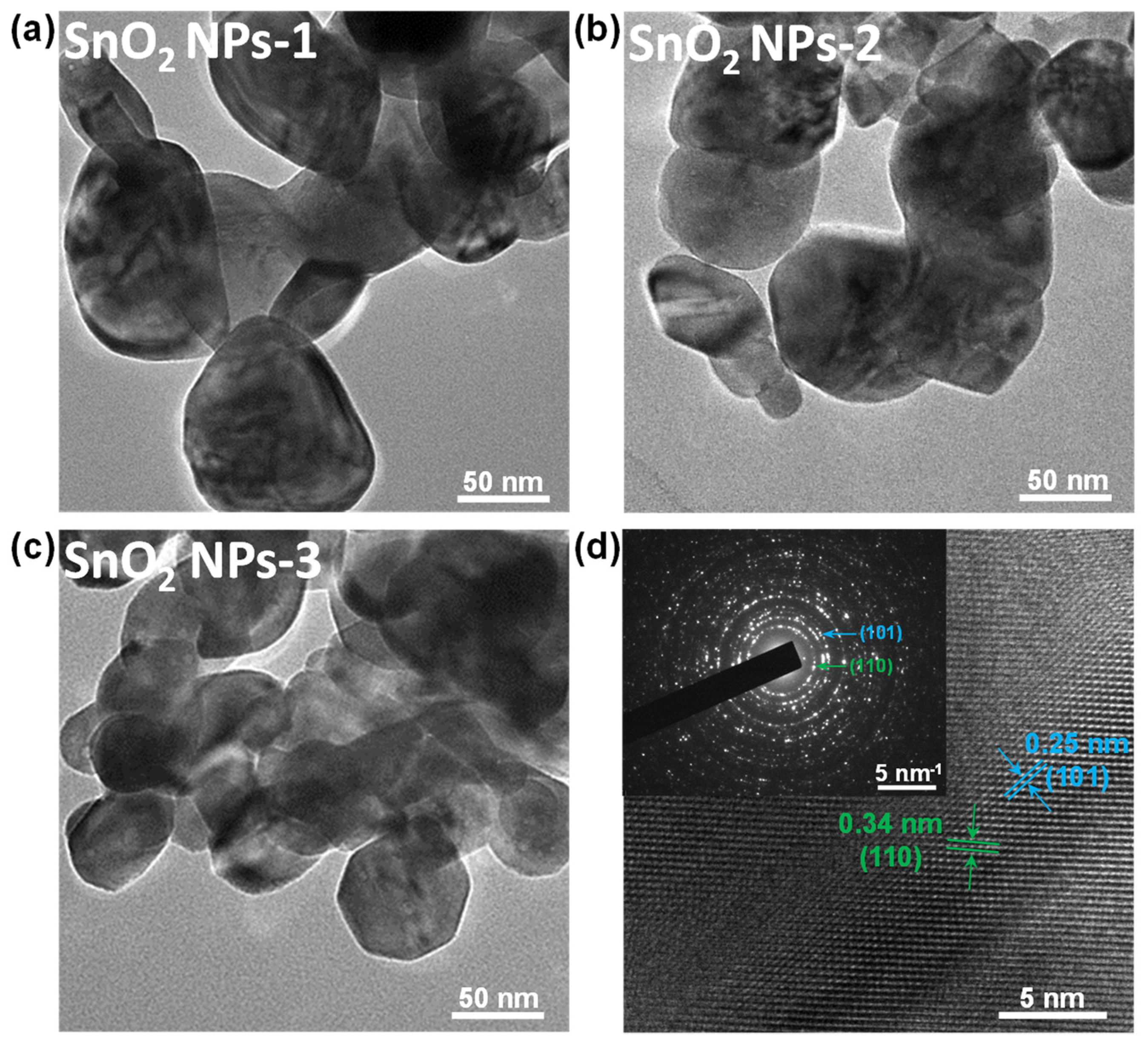
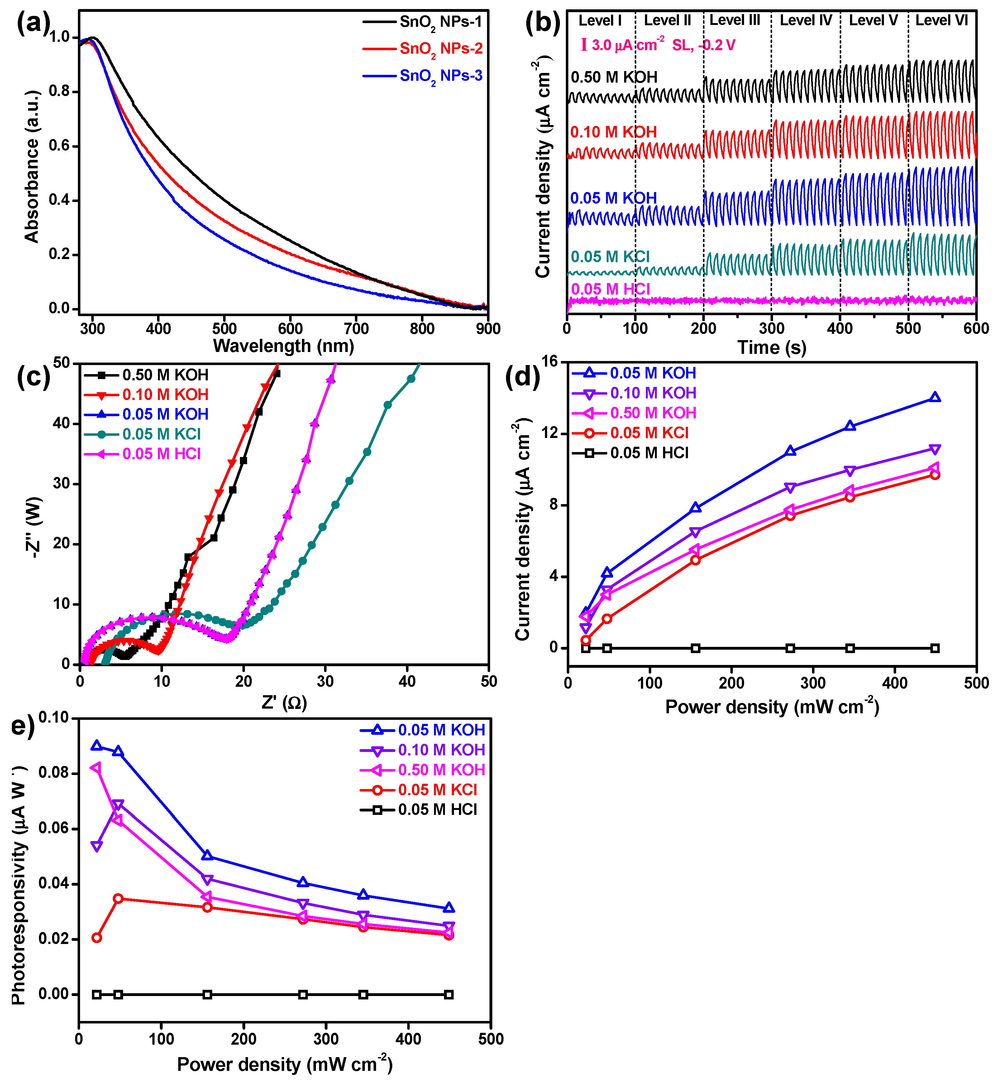
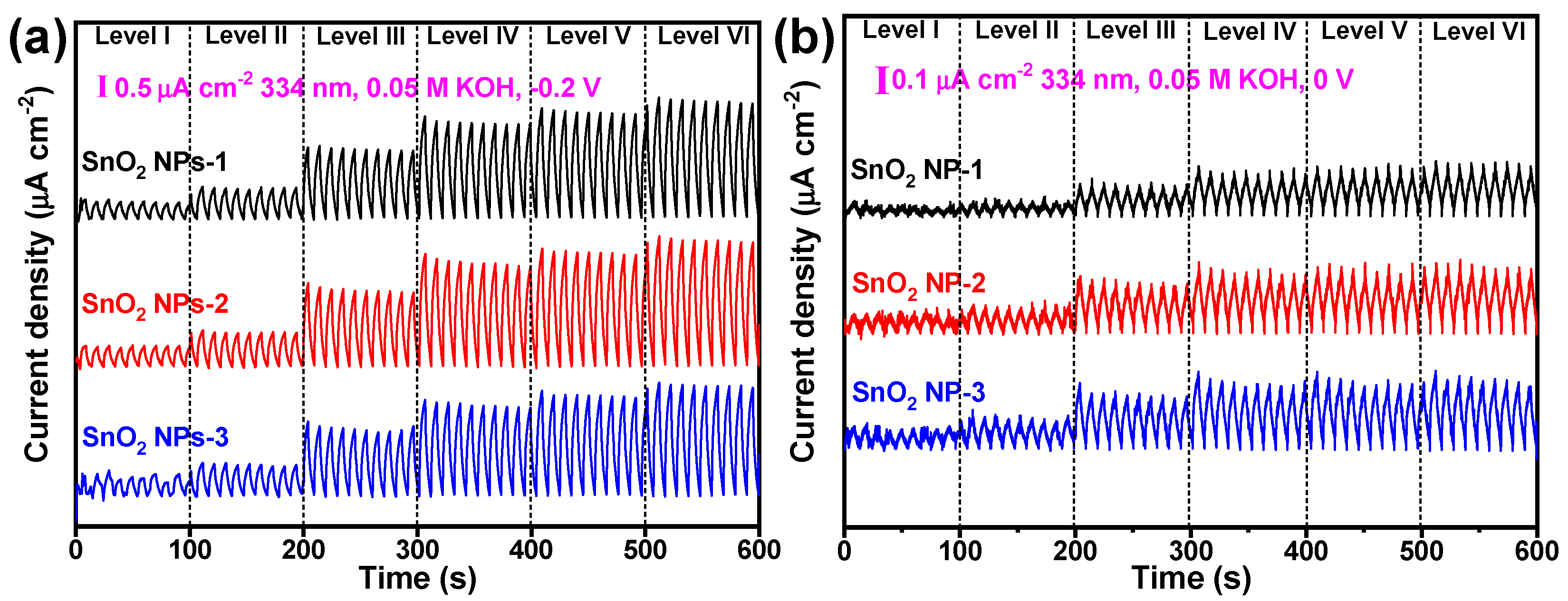
3. Results and Discussion

In this work, SnO2 nanostructures were fabricated by facile calcination on a large scale at relatively high temperature. The XRD results in Figure 1a show that only a high calcination temperature and a long calcination time, e.g., 700 °C for 8 h, could efficiently facilitate the formation of pure SnO2 structures. However, low calcination temperature or a short calcination time, e.g., calcination at 700 °C for 4 h or 600 °C for 8 h could lead to the formation of SnO structures to some extent, as shown by the appearance of the peak at ~30° caused by the insufficient decomposition of tin (II) oxalate powder, which can be indexed to the characteristic peak of SnO (Figure 1a) [37,38]. It can be observed from the SEM image that relatively uniform SnO2 nanostructures were obtained (Figure 1b), with diameters ranging from ~20 nm to ~150 nm (Figure 1c).
In order to obtain size-selected SnO2 NPs, a combination of LPE and LCC techniques was used. The LPE technique was used to exfoliate the SnO2 nanostructures calcined at 700 °C for 8 h, and the LCC technique was used to collect the as-exfoliated SnO2 NPs with a more uniform size. As shown in Figure 2, the TEM image shows that the SnO2 NPs obtained by a combination of LPE and LCC techniques displayed clear size selection, i.e., SnO2 NPs-1 collected at a centrifugation speed range from 2000 rps to 3000 rps had an average diameter of ~92 nm (Figure 2a); SnO2 NPs-2 collected at a centrifugation speed range from 5000 rps to 6000 rps had an average diameter of ~78 nm (Figure 2b); and SnO2 NPs-3 collected at a centrifugation speed range from 9000 rps to 10,000 rps had an average diameter of ~56 nm (Figure 2c). The HRTEM image shows clear lattice fringes of 0.25 nm and 0.34 nm (Figure 2d), which can be assigned to the (101) and (110) planes of the SnO2 crystals, respectively [29,39]. The selected-area electron diffraction (SAED) pattern (Figure 2d, inset) further confirms the formation of the SnO2 nanostructures.
UV–Vis–NIR absorption spectroscopy was employed to characterize the optical response of the size-selected SnO2 NPs, as shown in Figure 3a. It can be seen that all the three samples displayed a relatively narrow optical absorption, but with an increase in size of the SnO2 NPs the absorption became wider and stronger, in good agreement with the results reported for tin (II) sulfide (SnS) nanosheets [40] and tungsten disulfide (WS2) nanosheets [41]. Moreover, simulated light (SL, 300–2000 nm, Table S1) was employed as incident light to illuminate the SnO2-NP-based electrode for electricity detection. As shown in Figure 3b,c, except for the acidic electrolyte condition, the electrode always exhibited a gradually increasing photoresponse signal with an increase in the power density (Pλ) of SL in alkaline or neutral electrolyte, indicating that the performance optimization of this SnO2-NP-based photodetector can be easily realized. The influence of the electrolyte on the photoresponse behavior was also studied, as shown in Figure 3b,c. It can be observed that the alkaline electrolyte was the most competitive electrolyte in this SnO2-NP-based photodetector, because the highest photocurrent density (I = (IonIoff)/S) was delivered in 0.05 M KOH compared with those delivered in 0.05 M KCl and 0.05 M KCl. Here, Ion and Ioff denote the photocurrent with and without irradiation, respectively, and S represents the effective area of the SnO2 NPs under irradiation. This could be mainly attributable to the different functionalities of the SnO2 NPs on the surface and the electrolytes, due to the similar resistance interface (R) between the SnO2 NPs and the electrolytes (R0.05M KOH = 17.6 Ω, R0.05M KCl = 18.3 Ω, and R0.05M HCl = 17.6 Ω), as seen in Figure 3d. It is noted that the highest I in this work reached 14.0 μA cm−2, significantly outperforming black phosphorus nanosheets (0.382 μA cm−2) [11] and black phosphorus analogue nanomaterials such as tin (II) sulfide nanosheets (1.59 μA cm−2) [40] and tellurene (0.365 μA cm−2) [12] (Table S2). Furthermore, the electrolyte concentration also played an important role in the photoresponse behavior. It can be observed from Figure 3b,c that the lower the KOH concentration, the higher the value of I, which could be mainly ascribed to the R (R0.50M KOH = 5.5 Ω, R0.10M KOH = 8.7 Ω, and R0.05M KOH = 17.6 Ω), as seen in Figure 3d, indicating that at the studied electrolyte concentrations, high electrolyte concentration severely suppressed the efficient separation of hole (h+)–electron (e) pairs. In addition, unlike for I, larger photoresponsivity (R = I/Pλ) was usually obtained under relatively low Pλ, especially in KOH electrolytes (0.05 M, 0.10 M, and 0.50 M), as seen in Figure 3e. The highest R value reached 0.10 μA W−1, which is comparable to those of black phosphorus nanosheets (2.2 μA W−1) [11] and tellurene (3.0 μA W−1) [12]. It should be noted that the much larger Pλ of SL employed in this work leads to low values of R compared to those reported in other studies [6,42].
In order to emphasize the specific response behavior in the UV region, incident lasers with different wavelengths (300, 334, 380, and 420 nm) were used to irradiate the SnO2-NP-based electrodes. As shown in Figure 4a, the as-prepared SnO2-NP-based electrode displayed significantly the largest I under the 334 nm laser, compared with the values under 300, 380, or 420 nm lasers under the same conditions, verifying that this SnO2-NP-based photodetector has a specific UV photodetection performance. The largest I and R values, observed under the 334 nm laser at an external voltage of −0.2 V, were 5.35 μA cm−2 and 4.61 μA W−1, respectively. Note that this specific UV photodetection performance under a 300 nm or 334 nm laser does not dramatically deteriorate when the external voltage changes remarkably (see Figure S1). The response time (tres) and recovery time (trec) are usually assigned to the time interval for the rise and decay from 10% to 90% and from 90% to 10% of the peak value, respectively [40]. It can be seen in Figure 4b and Figure S2 that the tres/trec of the as-fabricated SnO2-NP-1-based electrode was 2.7 s/3.8 s, close to those of the SnO2-NP-2-based electrode (3.6 s/3.9 s) and the SnO2-NP-3-based electrode (3.5 s/3.8 s), all of which are comparable to those of SnSe nanosheets (1.2 s/2.2 s) [43] and bismuth selenide nanosheets (5.3 s/9.5 s) [44].
Due to the size-dependent absorption of the SnO2 NPs as mentioned above and seen in Figure 2a, the photoresponse behavior and self-powered photoresponse performance (zero external voltage) were also studied, as shown in Figure 5. It can be seen from Figure 5a and Figure S3 that the photocurrent densities of SnO2 NPs-2 and SnO2 NPs-3 irradiated by SL (Figure 5a) and the 334 nm laser (Figure S3) at an applied exteral voltage were almost the same under the same conditions, while they were evidently superior to that of SnO2 NPs-1, indicating that relatively smaller SnO2 NPs were more beneficial for strengthening the PEC signal. Similarly, at zero external voltage, the self-powered photoresponse signal had the same trend as at −0.2 V (Figure 5b), and the largest self-powered I was 2.25 μA cm−2, which is also better than that of black phosphorus nanosheets (0.265 μA cm−2) [11] and selenium quantum dots (0.0385 μA cm−2) [14]. In addition, the reduction in I after one month was calculated to be only 27.6% (Table S2 and Figure S4), and the observed on/off switching behavior was unchanged from the beginning. This, combined with almost the same color before and after measurement (Figure S5), confirmed that the as-prepared SnO2-NP-based electrode shows excellent photoresponse stability and holds great potential for practical applications in optoelectronic devices.

4. Conclusions

In this contribution, SnO2 NPs were facilely fabricated by calcination of tin (II) oxalate in air, followed by a combination of LPE and LCC techniques. The XRD patterns showed that the SnO2 nanostructures could be successfully obtained after sufficient calcination for 8 h at 700 °C. The SEM image showed that the as-fabricated SnO2 NPs had a particle size ranging from ~20 nm to ~150 nm. The PEC result demonstrated that the SnO2-NP-based electrode not only had a strong electrolyte-dependent PEC performance (i.e., the best performance in a low-concentration alkaline electrolyte), but also exhibited size-modulated photoresponse behavior, i.e., the smaller the size, the better the PEC performance. Moreover, the SnO2-NP-based photodetector showed a much stronger and more stable PEC signal in the UV region (300 nm and 334 nm), compared to that in the visible region (420 nm), indicating that it has great potential as a building block in UV photodetectors. In addition, the excellent PEC stability even for a one-month PEC measurement makes the SnO2-NP-based electrode a promising candidate for practical applications. It is anticipated that the present work can provide fundamental guidance on the performance of a PEC-type SnO2-NP-based photodetector and offer extensive availabilities for high-performance SnO2-based heterostructures for constructing next-generation optoelectronic devices.

Supplementary Materials

The following supporting information can be downloaded at: https://www.mdpi.com/article/10.3390/nano12040632/s1, Table S1: Laser power density (Pλ) of of incident light with various irradiation wavelengths; Table S2: The comparison of the SnO2 NP-based PEC electrodes and other published PEC electrodes; Figure S1: The influence of laser wavelength on the on/off switching behavior of the as-fabricated SnO2 NPs at −0.4 V; Figure S2: The response time and decay time of (a) the as-fabricated SnO2 NP-2 and (b) SnO2 NP-3-based electrodes irradiated by SL in 0.05 M KOH: Figure S3: Size effect of the SnO2 NPs with different sizes on the photoresponse behavior at external voltages of −0.4 V under 334 nm laser; Figure S4: (a) Photoresponse stability of the as-prepared SnO2 NPs-1, and (b) its enlarged area; Figure S5: The pictures of (a) the as-prepared SnO2 NP-1 powder and (b) SnO2 NP-1-based electrode.

Author Contributions

Z.H. and Y.Z. (Yueping Zhu) conducted the experiments to collect the data and drafted the manuscript; Z.H., J.Z. and Y.H. fabricated the devices and performed the measurements; Y.Z. (Yueping Zhu), G.Z., L.H., Y.Z. (You Zi) and W.H. made significant contributions to the revision of the experimental design and manuscript editing, guiding the entire study. All authors have read and agreed to the published version of the manuscript.

Funding

The research was supported by the National Natural Science Foundation of China (Grant Nos. 61805147, 22005158, and 52103316).

Data Availability Statement

The data presented in this study are available on request from the corresponding author.

Conflicts of Interest

The authors declare no conflict of interest.

References

  1. Wang, M.; Zhu, J.; Zi, Y.; Wu, Z.-G.; Hu, H.; Xie, Z.; Zhang, Y.; Hu, L.; Huang, W. Functional Two-Dimensional Black Phosphorus Nanostructures towards Next-Generation Devices. J. Mater. Chem. A 2021, 9, 12433–12473. [Google Scholar] [CrossRef]
  2. Wang, M.; Zhu, J.; Zi, Y.; Huang, W. 3D MXene Sponge: Facile Synthesis, Excellent Hydrophobicity, and High Photothermal Efficiency for Waste Oil Collection and Purification. ACS Appl. Mater. Interfaces 2021, 13, 47302–47312. [Google Scholar] [CrossRef] [PubMed]
  3. Wang, M.; Zi, Y.; Zhu, J.; Huang, W.; Zhang, Z.; Zhang, H. Construction of Super-Hydrophobic PDMS@MOF@Cu Mesh for Reduced Drag, Anti-Fouling and Self-Cleaning towards Marine Vehicle Applications. Chem. Eng. J. 2021, 417, 129265. [Google Scholar] [CrossRef]
  4. Huang, W.; Hu, L.; Tang, Y.; Xie, Z.; Zhang, H. Recent Advances in Functional 2D MXene-Based Nanostructures for Next-Generation Devices. Adv. Funct. Mater. 2020, 30, 2005223. [Google Scholar] [CrossRef]
  5. Mohanta, D.; Ahmaruzzaman, M. A Novel Au-SnO2-rGO Ternary Nanoheterojunction Catalyst for UV-LED Induced Photocatalytic Degradation of Clothianidin: Identification of Reactive Intermediates, Degradation Pathway and In-Depth Mechanistic Insight. J. Hazard. Mater. 2020, 397, 122685. [Google Scholar] [CrossRef] [PubMed]
  6. Huang, W.; Zhang, Y.; You, Q.; Huang, P.; Wang, Y.; Huang, Z.N.; Ge, Y.; Wu, L.; Dong, Z.; Dai, X.; et al. Enhanced Photodetection Properties of Tellurium@Selenium Roll-to-Roll Nanotube Heterojunctions. Small 2019, 15, 1900902. [Google Scholar] [CrossRef]
  7. Li, Z.; Sun, L.; Liu, Y.; Zhu, L.; Yu, D.; Wang, Y.; Sun, Y.; Yu, M. SnSe@SnO2 Core-Shell Nanocomposite for Synchronous Photothermal-Photocatalytic Production of Clean Water. Environ. Sci. Nano 2019, 6, 1507–1515. [Google Scholar] [CrossRef]
  8. Xing, C.; Chen, X.; Huang, W.; Song, Y.; Li, J.; Chen, S.; Zhou, Y.; Dong, B.; Fan, D.; Zhu, X.; et al. Two-Dimensional Lead Monoxide: Facile Liquid Phase Exfoliation, Excellent Photoresponse Performance, and Theoretical Investigation. ACS Photonics 2018, 5, 5055–5067. [Google Scholar] [CrossRef]
  9. Uddin, M.T.; Nicolas, Y.; Olivier, C.; Toupance, T.; Servant, L.; Müller, M.M.; Kleebe, H.-J.; Ziegler, J.; Jaegermann, W. Nanostructured SnO2-ZnO Heterojunction Photocatalysts Showing Enhanced Photocatalytic Activity for the Degradation of Organic Dyes. Inorg. Chem. 2012, 51, 7764–7773. [Google Scholar] [CrossRef]
  10. Huang, W.; Li, C.; Gao, L.; Zhang, Y.; Wang, Y.; Huang, Z.N.; Chen, T.; Hu, L.; Zhang, H. Emerging Black Phosphorus Analogue Nanomaterials for High-Performance Device Applications. J. Mater. Chem. C 2020, 8, 1172–1197. [Google Scholar] [CrossRef]
  11. Ren, X.; Li, Z.; Huang, Z.; Sang, D.; Qiao, H.; Qi, X.; Li, J.; Zhong, J.; Zhang, H. Environmentally Robust Black Phosphorus Nanosheets in Solution: Application for Self-Powered Photodetector. Adv. Funct. Mater. 2017, 27, 1606834. [Google Scholar] [CrossRef]
  12. Xie, Z.; Xing, C.; Huang, W.; Fan, T.; Li, Z.; Zhao, J.; Xiang, Y.; Guo, Z.; Li, J.; Yang, Z.; et al. Ultrathin 2D Nonlayered Tellurium Nanosheets: Facile Liquid-Phase Exfoliation, Characterization, and Photoresponse with High Performance and Enhanced Stability. Adv. Funct. Mater. 2018, 28, 1705833. [Google Scholar] [CrossRef]
  13. Huang, W.; Wang, M.; Hu, L.; Wang, C.; Xie, Z.; Zhang, H. Recent Advances in Semiconducting Monoelemental Selenium Nanostructures for Device Applications. Adv. Funct. Mater. 2020, 30, 2003301. [Google Scholar] [CrossRef]
  14. Jiang, X.; Huang, W.; Wang, R.; Li, H.; Xia, X.; Zhao, X.; Hu, L.; Chen, T.; Tang, Y.; Zhang, H. Photocarrier Relaxation Pathways in Selenium Quantum Dots and Their Application in UV-Vis Photodetection. Nanoscale 2020, 12, 11232–11241. [Google Scholar] [CrossRef] [PubMed]
  15. Wang, Y.; Qiu, G.; Wang, R.; Huang, S.; Wang, Q.; Liu, Y.; Du, Y.; Goddard III, W.A.; Kim, M.J.; Xu, X.; et al. Field-Effect Transistors Made from Solution-Grown Two-Dimensional Tellurene. Nat. Electron. 2018, 1, 228–236. [Google Scholar] [CrossRef]
  16. Sang, L.; Liao, M.; Sumiya, M. A Comprehensive Review of Semiconductor Ultraviolet Photodetectors: From Thin Film to One-Dimensional Nanostructures. Sensors 2013, 13, 10482–10518. [Google Scholar] [CrossRef]
  17. Liao, M.; Sang, L.; Teraji, T.; Imura, M.; Alvarez, J.; Koide, Y. Comprehensive Investigation of Single Crystal Diamond Deep-Ultraviolet Detectors. Jpn. J. Appl. Phys. 2012, 51, 090115. [Google Scholar] [CrossRef] [Green Version]
  18. Hu, K.; Teng, F.; Zheng, L.; Yu, P.; Zhang, Z.; Chen, H.; Fang, X. Binary Response Se/ZnO p-n Heterojunction UV Photodetector with High On/Off Ratio and Fast Speed. Laser Photonics Rev. 2017, 11, 1600257. [Google Scholar] [CrossRef]
  19. Huang, Y.; Yu, Q.; Wang, J.; Wang, J.; Yu, C.; Abdalla, J.T.; Zeng, Z.; Jiao, S.; Wang, D.; Gao, S. Plasmon-Enhanced Self-Powered UV Photodetectors Assembled by Incorporating Ag@SiO2 Core-Shell Nanoparticles into TiO2 Nanocube Photoanodes. ACS Sustain. Chem. Eng. 2018, 6, 438–446. [Google Scholar] [CrossRef]
  20. Chen, H.; Liu, H.; Zhang, Z.; Hu, K.; Fang, X. Nanostructured Photodetectors: From Ultraviolet to Terahertz. Adv. Mater. 2016, 28, 403–433. [Google Scholar] [CrossRef]
  21. Song, Z.; Wei, Z.; Wang, B.; Luo, Z.; Xu, S.; Zhang, W.; Yu, H.; Li, M.; Huang, Z.; Zang, J.; et al. Sensitive Room-Temperature H2S Gas Sensors Employing SnO2 Quantum Wire/Reduced Graphene Oxide Nanocomposites. Chem. Mater. 2016, 28, 1205–1212. [Google Scholar] [CrossRef]
  22. Ren, X.; Liu, Y.; Lee, D.G.; Kim, W.B.; Han, G.S.; Jung, H.S.; Liu, S. Chlorine-Modified SnO2 Electron Transport Layer for High-Efficiency Perovskite Solar Cells. InfoMat 2020, 2, 401–408. [Google Scholar] [CrossRef] [Green Version]
  23. Shen, A.; Zhang, Z.; Zhang, H.; Zhao, Y.; Xu, P.; Zhou, Y.; Weng, Y. Core-Etched CC/SnO2 Nanotube Arrays as High-Performance Anodes for Lithium-Ion Batteries with Ionic Liquid Electrolyte. Front. Mater. 2020, 7, 63. [Google Scholar] [CrossRef]
  24. Zhou, X.; Wan, L.-J.; Guo, Y.-G. Binding SnO2 Nanocrystals in Nitrogen-Doped Graphene Sheets as Anode Materials for Lithium-Ion Batteries. Adv. Mater. 2013, 25, 2152–2157. [Google Scholar] [CrossRef]
  25. Yu, H.; Tan, X.; Sun, S.; Zhang, L.; Gao, C.; Ge, S. Engineering Paper-Based Visible Light-Responsive Sn-Self Doped Domed SnO2 Nanotubes for Ultrasensitive Photoelectrochemical Sensor. Biosens. Bioelectron. 2021, 185, 113250. [Google Scholar] [CrossRef]
  26. Kalidoss, R.; Umapathy, S.; Anandan, R.; Ganesh, V.; Sivalingam, Y. Comparative Study on the Preparation and Gas Sensing Properties of Reduced Graphene Oxide/SnO2 Binary Nanocomposite for Detection of Acetone in Exhaled Breath. Anal. Chem. 2019, 91, 5116–5124. [Google Scholar] [CrossRef]
  27. Wu, J.; Zhao, R.; Xiang, H.; Yang, C.; Zhong, W.; Zhang, C.; Zhang, Q.; Li, X.; Yang, N. Exposing Highly Active (100) Facet on a SnS2/SnO2 Electrocatalyst to Boost Efficient Hydrogen Evolution. Appl. Catal. B Environ. 2021, 292, 120200. [Google Scholar] [CrossRef]
  28. Sudrajat, H.; Hartuti, S.; Babel, S.; Nguyen, T.K.; Tong, H.D. SnO2/ZnO Heterostructured Nanorods: Structural Properties and Mechanistic Insights into the Enhanced Photocatalytic Activity. J. Phys. Chem. Solid. 2021, 149, 109762. [Google Scholar] [CrossRef]
  29. Li, Z.; Wang, R.; Xue, J.; Xing, X.; Yu, C.; Huang, T.; Chu, J.; Wang, K.-L.; Dong, C.; Wei, Z.; et al. Core-Shell ZnO@SnO2 Nanoparticles for Efficient Inorganic Perovskite Solar Cells. J. Am. Chem. Soc. 2019, 141, 17610–17616. [Google Scholar] [CrossRef]
  30. Yu, H.; Dou, D.; Zhao, J.; Pang, B.; Zhang, L.; Chi, Z.; Yu, H. The exploration of Ti/SnO2-Sb Anode/Air Diffusion Cathode/UV Dual Photoelectric Catalytic Coupling System for the Biological Harmless Treatment of Real Antibiotic Industrial Wastewater. Chem. Eng. J. 2021, 412, 128581. [Google Scholar] [CrossRef]
  31. Yang, C.; Fan, Y.; Li, P.; Gu, Q.; Li, X.-y. Freestanding 3-Dimensional Macro-Porous SnO2 Electrodes for Efficient Electrochemical Degradation of Antibiotics in Wastewater. Chem. Eng. J. 2021, 422, 130032. [Google Scholar] [CrossRef]
  32. Singh, A.V.; Jahnke, T.; Xiao, Y.; Wang, S.; Yu, Y.; David, H.; Richter, G.; Laux, P.; Luch, A.; Srivastava, A.; et al. Peptide-Induced Biomineralization of Tin Oxide (SnO2) Nanoparticles for Antibacterial Applications. J. Nanosci. Nanotechnol. 2019, 19, 5674–5686. [Google Scholar] [CrossRef] [PubMed]
  33. Pandiyan, R.; Mahalingam, S.; Ahn, Y.-H. Antibacterial and Photocatalytic Activity of Hydrothermally Synthesized SnO2 Doped GO and CNT under Visible Light Irradiation. J. Photochem. Photobiol. B Biol. 2019, 191, 18–25. [Google Scholar] [CrossRef] [PubMed]
  34. Pakdel, A.; Bando, Y.; Golberg, D. Nano Boron Nitride Flatland. Chem. Soc. Rev. 2014, 43, 934–959. [Google Scholar] [CrossRef] [PubMed]
  35. Huang, W.; Jiang, X.; Wang, Y.; Zhang, F.; Ge, Y.; Zhang, Y.; Wu, L.; Ma, D.; Li, Z.; Wang, R.; et al. Two-Dimensional Beta-Lead Oxide Quantum Dots. Nanoscale 2018, 10, 20540–20547. [Google Scholar] [CrossRef]
  36. Huang, W.; Xing, C.; Wang, Y.; Li, Z.; Wu, L.; Ma, D.; Dai, X.; Xiang, Y.; Li, J.; Fan, D.; et al. Facile Fabrication and Characterization of Two-Dimensional Bismuth(III) Sulfide Nanosheets for High-Performance Photodetector Applications under Ambient Conditions. Nanoscale 2018, 10, 2404–2412. [Google Scholar] [CrossRef]
  37. Guo, Z.; Han, X.; Zhang, Z.; Zhang, X.; Liang, M.; Wu, D.; Yuan, W. High Active Crystalline {110} Facets with High Surface Energy in Tin Monoxide Photocatalyst. Inorg. Chem. Commun. 2021, 134, 109043. [Google Scholar] [CrossRef]
  38. Gu, J.; Héroguel, F.; Luterbacher, J.; Hu, X. Densely Packed, Ultra Small SnO Nanoparticles for Enhanced Activity and Selectivity in Electrochemical CO2 Reduction. Angew. Chem. Int. Ed. 2018, 57, 2943–2947. [Google Scholar] [CrossRef] [Green Version]
  39. Liu, H.; Chen, Z.; Wang, H.; Ye, F.; Ma, J.; Zheng, X.; Gui, P.; Xiong, L.; Wen, J.; Fang, G. A Facile Room Temperature Solution Synthesis of SnO2 Quantum Dots for Perovskite Solar Cells. J. Mater. Chem. A 2019, 7, 10636–10643. [Google Scholar] [CrossRef]
  40. Huang, W.; Xie, Z.; Fan, T.; Li, J.; Wang, Y.; Wu, L.; Ma, D.; Li, Z.; Ge, Y.; Huang, Z.N.; et al. Black-Phosphorus-Analogue Tin Monosulfide: An Emerging Optoelectronic Two-Dimensional Material for High-Performance Photodetection with Improved Stability under Ambient/Harsh Conditions. J. Mater. Chem. C 2018, 6, 9582–9593. [Google Scholar] [CrossRef]
  41. Backes, C.; Szydłowska, B.M.; Harvey, A.; Yuan, S.; Vega-Mayoral, V.; Davies, B.R.; Zhao, P.-l.; Hanlon, D.; Santos, E.J.G.; Katsnelson, M.I.; et al. Production of Highly Monolayer Enriched Dispersions of Liquid-Exfoliated Nanosheets by Liquid Cascade Centrifugation. ACS Nano 2016, 10, 1589–1601. [Google Scholar] [CrossRef] [PubMed]
  42. Zi, Y.; Zhu, J.; Wang, M.; Hu, L.; Hu, Y.; Wageh, S.; Al-Hartomy, O.A.; Al-Ghamdi, A.; Huang, W.; Zhang, H. CdS@CdSe Core/Shell Quantum Dots for Highly Improved Self-Powered Photodetection Performance. Inorg. Chem. 2021, 60, 18608–18613. [Google Scholar] [CrossRef] [PubMed]
  43. Li, F.; Chen, H.; Xu, L.; Zhang, F.; Yin, P.; Yang, T.; Shen, T.; Qi, J.; Zhang, Y.; Li, D.; et al. Defect Engineering in Ultrathin SnSe Nanosheets for High-Performance Optoelectronic Applications. ACS Appl. Mater. Interfaces 2021, 13, 33226–33236. [Google Scholar] [CrossRef] [PubMed]
  44. Zang, C.; Qi, X.; Ren, L.; Hao, G.; Liu, Y.; Li, J.; Zhong, J. Photoresponse Properties of Ultrathin Bi2Se3 Nanosheets Synthesized by Hydrothermal Intercalation and Exfoliation Route. Appl. Surf. Sci. 2014, 316, 341–347. [Google Scholar] [CrossRef]
Figure 1. Structural characterization of the SnO2 nanostructures. (a) XRD patterns of the sample prepared by calcination of SnC2O4 at different temperatures for a predetermined time in air. (b) SEM image of SnO2 nanostructures obtained by calcination of SnC2O4 at 700 °C for 8 h in air and (c) the enlarged area corresponding to the region surrounded by a green box in (b).
Nanomaterials 12 00632 g001
Figure 2. TEM characterization of the SnO2 NPs with different sizes: (a) SnO2 NPs-1, (b) SnO2 NPs-2, (c) SnO2 NPs-3. (d) HRTEM image; inset shows its SAED pattern.
Nanomaterials 12 00632 g002
Figure 3. Photoresponse behavior. (a) UV–Vis–NIR spectra of the size-selected SnO2 NPs; (b) on/off switching behavior of the SnO2-NPs-1-based electrode in different electrolytes under SL at −0.2 V; (c) current density of the SnO2-NPs-1-based electrode as a function of power density; (d) interface resistances between the SnO2-NPs-1-based electrode and different electrolytes; (e) photoresponsivity of the SnO2-NPs-1-based electrode as a function of power density.
Nanomaterials 12 00632 g003
Figure 4. (a) The influence of laser wavelength on the on/off switching behavior of the as-fabricated SnO2 NPs at −0.2 V and (b) response time and decay time.
Nanomaterials 12 00632 g004
Figure 5. Effect of SnO2 NPs with different sizes on the photoresponse behavior at external voltages of (a) −0.2 V and (b) 0 V, under SL.
Nanomaterials 12 00632 g005
Publisher’s Note: MDPI stays neutral with regard to jurisdictional claims in published maps and institutional affiliations.

