
Optimization and Characterization of Electrodeposited Cadmium Selenide on Monocrystalline Silicon

 ,
, 
 ,
,  ,
,  and
and 
Abstract
:1. Introduction
2. Materials and Methods
2.1. Electrochemical Measurements
2.2. Microscopic and Spectroscopic Characterization
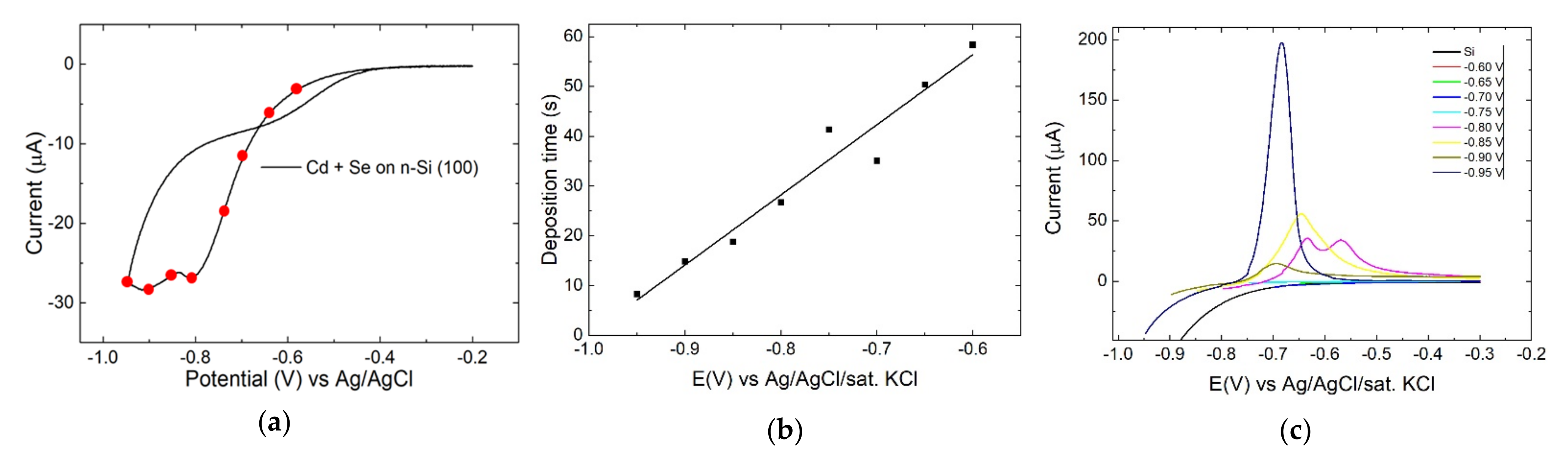
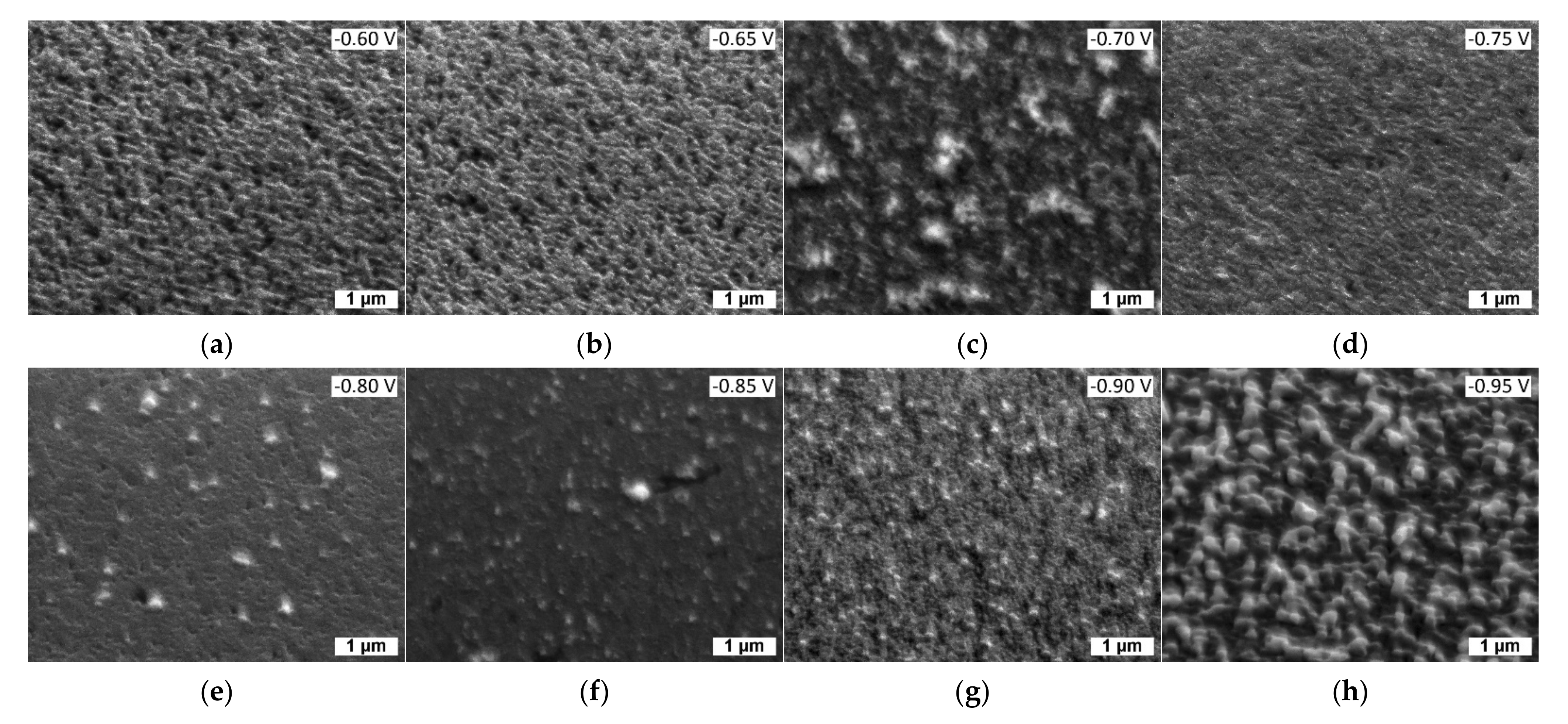
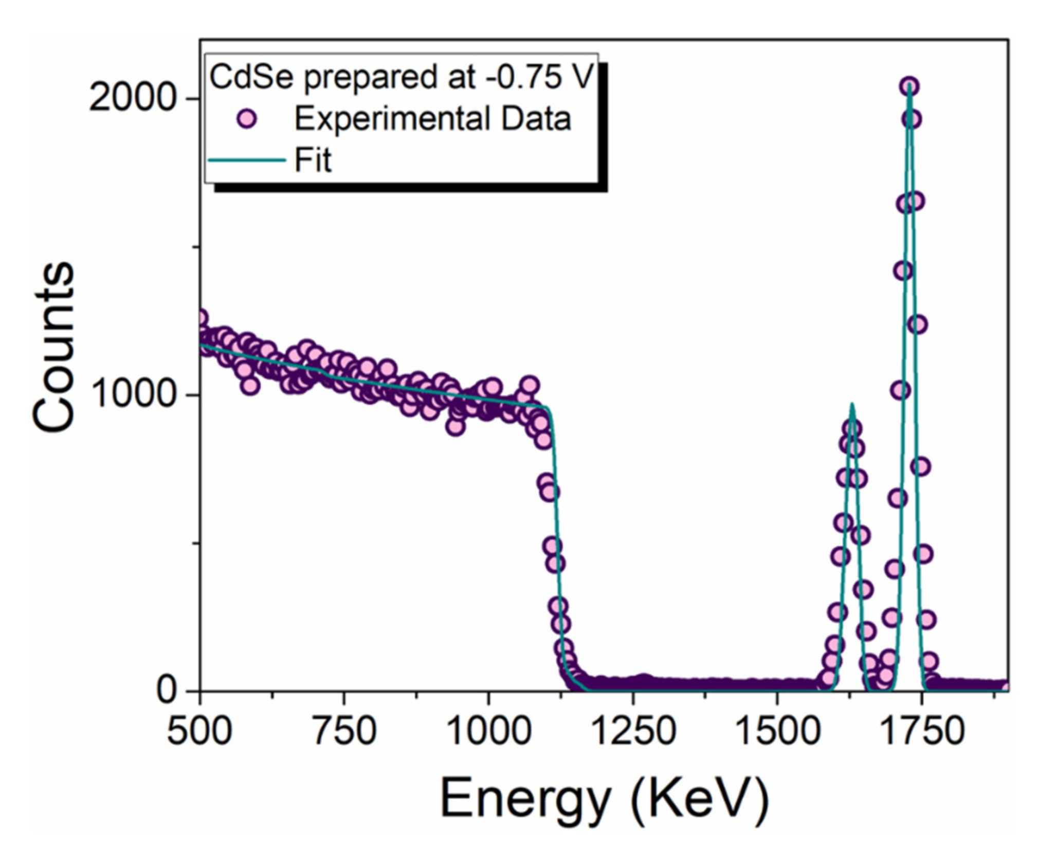
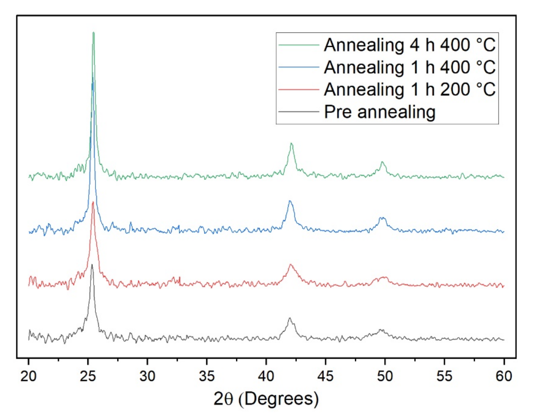
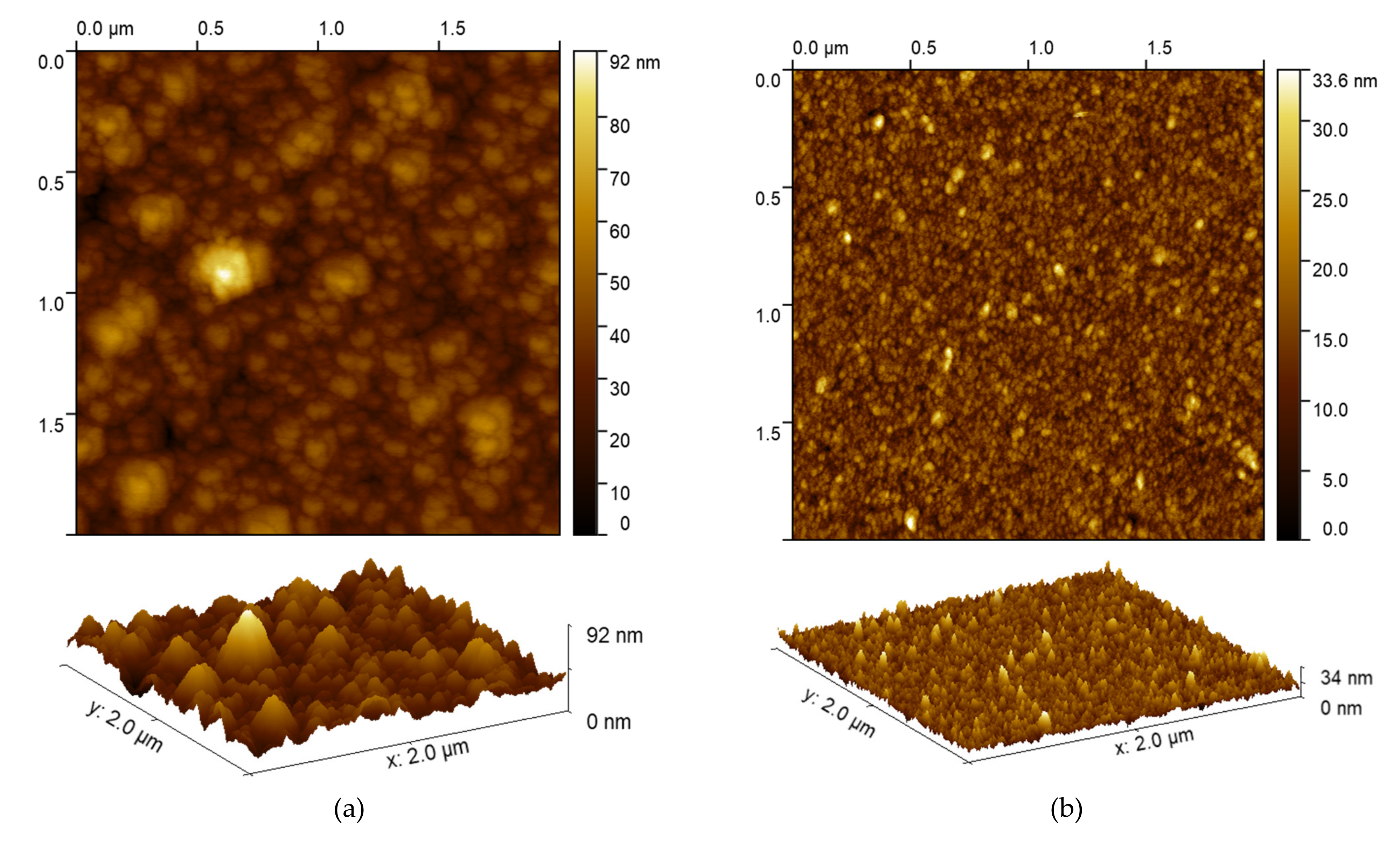
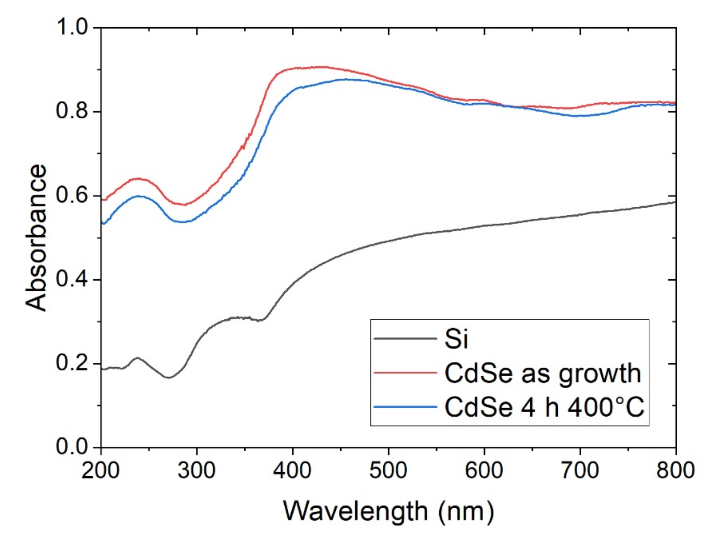
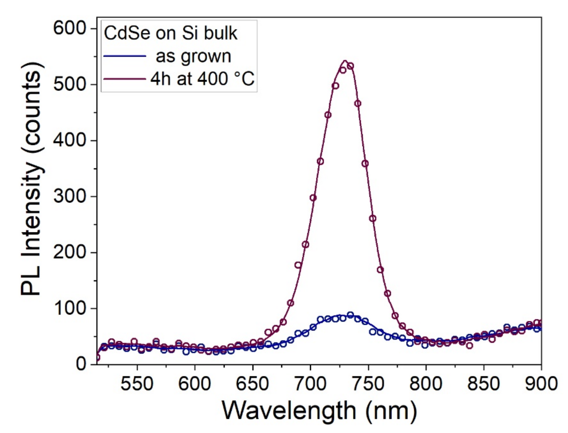
3. Results
4. Conclusions
Author Contributions
Funding
Institutional Review Board Statement
Informed Consent Statement
Data Availability Statement
Conflicts of Interest
References
- Kalem, S.; Werner, P.; Talalaev, V. Near-IR photoluminescence from Si/Ge nanowire-grown silicon wafers: Effect of HF treatment. Appl. Phys. A Mater. Sci. Process. 2013, 112, 561–567. [Google Scholar] [CrossRef] [Green Version]
- Wu, K.; Sun, W.; Jiang, Y.; Chen, J.; Li, L.; Cao, C.; Shi, S.; Shen, X.; Cui, J. Structure and photoluminescence study of silicon based two-dimensional Si2Te3 nanostructures. J. Appl. Phys. 2017, 122, 075701. [Google Scholar] [CrossRef]
- Iatsunskyi, I.; Pavlenko, M.; Viter, R.; Jancelewicz, M.; Nowaczyk, G.; Baleviciute, I.; Załęski, K.; Jurga, S.; Ramanavicius, A.; Smyntyna, V. Tailoring the Structural, Optical, and Photoluminescence Properties of Porous Silicon/TiO2 Nanostructures. J. Phys. Chem. C 2015, 119, 7164–7171. [Google Scholar] [CrossRef]
- Iacona, F.; Pacifici, D.; Irrera, A.; Miritello, M.; Franzò, G.; Priolo, F.; Sanfilippo, D.; Di Stefano, G.; Fallica, P.G. Electroluminescence at 1.54 μm in Er-doped Si nanocluster-based devices. Appl. Phys. Lett. 2002, 81, 3242–3244. [Google Scholar] [CrossRef]
- Talbot, E.; Lardé, R.; Pareige, P.; Khomenkova, L.; Hijazi, K.; Gourbilleau, F. Nanoscale evidence of erbium clustering in Er-doped silicon-rich silica. Nanoscale Res. Lett. 2013, 8, 1–8. [Google Scholar] [CrossRef] [Green Version]
- Gao, Y.; Shen, H.; Cao, J.; Li, D.; Yang, D. Control of the formation and luminescent properties of polymorphic erbium silicates on silicon. Opt. Mater. Express 2019, 9, 1716. [Google Scholar] [CrossRef]
- Leonardi, A.A.; Lo Faro, M.J.; Irrera, A. CMOS-Compatible and Low-Cost Thin Film MACE Approach for Light-Emitting Si NWs Fabrication. Nanomaterials 2020, 10, 966. [Google Scholar] [CrossRef]
- Walavalkar, S.S.; Hofmann, C.E.; Homyk, A.P.; Henry, M.D.; Atwater, H.A.; Scherer, A. Tunable visible and near-IR emission from sub-10 nm etched single-crystal Si nanopillars. Nano Lett. 2010, 10, 4423–4428. [Google Scholar] [CrossRef]
- Dohnalová, K.; Poddubny, A.N.; Prokofiev, A.A.; De Boer, W.D.; Umesh, C.P.; Paulusse, J.M.; Zuilhof, H.; Gregorkiewicz, T. Surface brightens up Si quantum dots: Direct bandgap-like size-tunable emission. Light Sci. Appl. 2013, 2, e47. [Google Scholar] [CrossRef]
- Leonardi, A.A.; Nastasi, F.; Morganti, D.; Lo Faro, M.J.; Picca, R.A.; Cioffi, N.; Franzò, G.; Serroni, S.; Priolo, F.; Puntoriero, F.; et al. New Hybrid Light Harvesting Antenna Based on Silicon Nanowires and Metal Dendrimers. Adv. Opt. Mater. 2020, 8, 2001070. [Google Scholar] [CrossRef]
- Lo Faro, M.J.; Leonardi, A.A.; Priolo, F.; Fazio, B.; Miritello, M.; Irrera, A. Erbium emission in Er:Y2O3 decorated fractal arrays of silicon nanowires. Sci. Rep. 2020, 10, 12854. [Google Scholar] [CrossRef]
- Karbassian, F.; Rajabali, S.; Chimeh, A.; Mohajerzadeh, S.; Asl-Soleimani, E. Luminescent porous silicon prepared by reactive ion etching. J. Phys. D. Appl. Phys. 2014, 47, 385103. [Google Scholar] [CrossRef]
- Gelloz, B.; Juangsa, F.B.; Nozaki, T.; Asaka, K.; Koshida, N.; Jin, L. Si/SiO2 Core/Shell Luminescent Silicon Nanocrystals and Porous Silicon Powders With High Quantum Yield, Long Lifetime, and Good Stability. Front. Phys. 2019, 7, 47. [Google Scholar] [CrossRef] [Green Version]
- Tsybeskov, L.; Lockwood, D.J. Silicon-germanium nanostructures for light emitters and on-chip optical interconnects. Proc. IEEE 2009, 97, 1284–1303. [Google Scholar] [CrossRef]
- Hambrock, J.; Birkner, A.; Fischer, R.A. Synthesis of CdSe nanoparticles using various organometallic cadmium precursors. J. Mater. Chem. 2001, 11, 3197–3201. [Google Scholar] [CrossRef]
- Ge, Y.; Zhang, M.; Wang, L.; Meng, L.; Tang, J.; Chen, Y.; Wang, L.; Zhong, H. Polarization-Sensitive Ultraviolet Detection from Oriented-CdSe@CdS-Dot-in-Rods-Integrated Silicon Photodetector. Adv. Opt. Mater. 2019, 7, 1–7. [Google Scholar] [CrossRef]
- Sun, M.; Zhang, S.; Wang, J.; Jia, Z.; Lv, X.; Huang, X. Enhanced biosensor based on assembled porous silicon microcavities using CdSe/ZnS quantum dots. IEEE Photonics J. 2021, 13, 1–6. [Google Scholar] [CrossRef]
- Li, K.; Lin, X.; Song, B.; Kondrotas, R.; Wang, C.; Lu, Y.; Yang, X.; Chen, C.; Tang, J. Rapid thermal evaporation for cadmium selenide thin-film solar cells. Front. Optoelectron. 2021, 14, 482–490. [Google Scholar] [CrossRef]
- Lopez-Delgado, R.; Zhou, Y.; Zazueta-Raynaud, A.; Zhao, H.; Pelayo, J.E.; Vomiero, A.; Álvarez-Ramos, M.E.; Rosei, F.; Ayon, A. Enhanced conversion efficiency in Si solar cells employing photoluminescent down-shifting CdSe/CdS core/shell quantum dots. Sci. Rep. 2017, 7, 14104. [Google Scholar] [CrossRef]
- Zhao, J.; Bardecker, J.A.; Munro, A.M.; Liu, M.S.; Niu, Y.; Ding, I.K.; Luo, J.; Chen, B.; Jen, A.K.Y.; Ginger, D.S. Efficient CdSe/CdS quantum dot light-emitting diodes using a thermally polymerized hole transport layer. Nano Lett. 2006, 6, 463–467. [Google Scholar] [CrossRef]
- Pal, B.N.; Ghosh, Y.; Brovelli, S.; Laocharoensuk, R.; Klimov, V.I.; Hollingsworth, J.A.; Htoon, H. ‘Giant’ CdSe/CdS Core/Shell Nanocrystal Quantum Dots As Efficient Electroluminescent Materials: Strong Influence of Shell Thickness on Light-Emitting Diode Performance. Nano Lett. 2011, 12, 331–336. [Google Scholar] [CrossRef]
- Bae, W.K.; Kwak, J.; Park, J.W.; Char, K.; Lee, C.; Lee, S. Highly Efficient Green-Light-Emitting Diodes Based on CdSe@ZnS Quantum Dots with a Chemical-Composition Gradient. Adv. Mater. 2009, 21, 1690–1694. [Google Scholar] [CrossRef]
- Tarabrin, M.K.; Ustinov, D.V.; Tomilov, S.M.; Lazarev, V.A.; Karasik, V.E.; Kozlovsky, V.I.; Korostelin, Y.V.; Skasyrsky, Y.K.; Frolov, M.P. Highly efficient continuous wave single mode Cr:CdSe laser with output power more than 2 W. In Proceedings of the Laser Congress 2018 (ASSL); Optical Society of America: Boston, MA, USA, 2018; p. AW3A.8. [Google Scholar]
- Kozlovsky, V.I.; Korostelin, Y.V.; Podmar’kov, Y.P.; Skasyrsky, Y.K.; Frolov, M.P. Middle infrared Fe2+:ZnS, Fe2+:ZnSe and Cr2+:CdSe lasers: New results. J. Phys. Conf. Ser. 2016, 740, 012006. [Google Scholar] [CrossRef]
- Akimov, V.A.; Kozlovskii, V.I.; Korostelin, Y.V.; Landman, A.I.; Podmar’kov, Y.P.; Skasyrskii, Y.K.; Frolov, M.P. Efficient pulsed Cr2+:CdSe laser continuously tunable in the spectral range from 2.26 to 3.61 μm. Quantum Electron. 2008, 38, 205. [Google Scholar] [CrossRef]
- Ayvazian, T.; van der Veer, W.E.; Xing, W.; Yan, W.; Penner, R.M. Electroluminescent, Polycrystalline Cadmium Selenide Nanowire Arrays. ACS Nano 2013, 7, 9469–9479. [Google Scholar] [CrossRef]
- Ramrakhiani, M.; Nogriya, V. Photo- and electro-luminescence of cadmium selenide nanocrystals and nanocomposites. J. Lumin. 2013, 133, 129–134. [Google Scholar] [CrossRef]
- Freeman, R.; Finder, T.; Bahshi, L.; Gill, R.; Willner, I. Functionalized CdSe/ZnS QDs for the detection of nitroaromatic or RDX explosives. Adv. Mater. 2012, 24, 6416–6421. [Google Scholar] [CrossRef]
- Zhang, Y.; Xiao, J.-Y.; Zhu, Y.; Tian, L.-J.; Wang, W.-K.; Zhu, T.-T.; Li, W.-W.; Yu, H.-Q. Fluorescence Sensor Based on Biosynthetic CdSe/CdS Quantum Dots and Liposome Carrier Signal Amplification for Mercury Detection. Anal. Chem. 2020, 92, 3990–3997. [Google Scholar] [CrossRef]
- Sung, T.W.; Lo, Y.L. Ammonia vapor sensor based on CdSe/SiO2 core–shell nanoparticles embedded in sol–gel matrix. Sensors Actuators B Chem. 2013, 188, 702–708. [Google Scholar] [CrossRef]
- Li, Z.; Peng, X. Size/Shape-Controlled Synthesis of Colloidal CdSe Quantum Disks: Ligand and Temperature Effects. J. Am. Chem. Soc. 2011, 133, 6578–6586. [Google Scholar] [CrossRef]
- Baek, S.-W.; Shim, J.-H.; Seung, H.-M.; Lee, G.-S.; Hong, J.-P.; Lee, K.-S.; Park, J.-G. Effect of core quantum-dot size on power-conversion-efficiency for silicon solar-cells implementing energy-down-shift using CdSe/ZnS core/shell quantum dots. Nanoscale 2014, 6, 12524–12531. [Google Scholar] [CrossRef] [PubMed]
- Nguyen, H.T.; Tran, T.T.; Bhatt, V.; Kumar, M.; Song, J.; Yun, J.-H. Enhancement of Schottky Junction Silicon Solar Cell with CdSe/ZnS Quantum Dots Decorated Metal Nanostructures. Appl. Sci. 2021, 12, 83. [Google Scholar] [CrossRef]
- Kim, J.; Choi, S.; Noh, J.; Yoon, S.; Lee, S.; Noh, T.; Frank, A.J.; Hong, K. Synthesis of CdSe−TiO 2 Nanocomposites and Their Applications to TiO 2 Sensitized Solar Cells. Langmuir 2009, 25, 5348–5351. [Google Scholar] [CrossRef] [PubMed]
- Li, Z.; Jin, D.; Wang, Z. Synthesis of step-scheme In2Se3/CdSe nanocomposites photocatalysts for hydrogen production. Compos. Commun. 2021, 24, 100618. [Google Scholar] [CrossRef]
- Shaikh, A.V.; Mane, R.S.; Joo, O.S.; Han, S.H.; Pathan, H.M. Electrochemical deposition of cadmium selenide films and their properties: A review. J. Solid State Electrochem. 2017, 21, 2517–2530. [Google Scholar] [CrossRef]
- Kowalik, R.; Kazimierczak, H.; Zabiński, P. Electrodeposition of cadmium selenide. Mater. Sci. Semicond. Process. 2016, 50, 43–48. [Google Scholar] [CrossRef]
- Loglio, F.; Innocenti, M.; D’Acapito, F.; Felici, R.; Pezzatini, G.; Salvietti, E.; Foresti, M.L. Cadmium selenide electrodeposited by ECALE: Electrochemical characterization and preliminary results by EXAFS. J. Electroanal. Chem. 2005, 575, 161–167. [Google Scholar] [CrossRef]
- Foresti, M.L.; Milani, S.; Loglio, F.; Innocenti, M.; Pezzatini, G.; Cattarin, S. Ternary CdS x Se 1 x Deposited on Ag(111) by ECALE: Synthesis and Characterization. Langmuir 2005, 21, 6900–6907. [Google Scholar] [CrossRef]
- Salvietti, E.; Giurlani, W.; Foresti, M.L.; Passaponti, M.; Fabbri, L.; Marcantelli, P.; Caporali, S.; Martinuzzi, S.; Calisi, N.; Pedio, M.; et al. On the Contrasting Effect Exerted by a Thin Layer of CdS against the Passivation of Silver Electrodes Coated with Thiols. Surfaces 2018, 1, 29–42. [Google Scholar] [CrossRef] [Green Version]
- Vizza, M.; Giaccherini, A.; Giurlani, W.; Passaponti, M.; Cioffi, N.; Picca, R.A.; De Luca, A.; Fabbri, L.; Lavacchi, A.; Gambinossi, F.; et al. Successes and Issues in the Growth of Moad and MoSe2 on Ag(111) by the E-ALD Method. Metals 2019, 9, 122. [Google Scholar] [CrossRef] [Green Version]
- Giurlani, W.; Giaccherini, A.; Calisi, N.; Zangari, G.; Salvietti, E.; Passaponti, M.; Caporali, S.; Innocenti, M. Investigations on the Electrochemical Atomic Layer Growth of Bi2Se3 and the Surface Limited Deposition of Bismuth at the Silver Electrode. Materials 2018, 11, 1426. [Google Scholar] [CrossRef] [Green Version]
- Giurlani, W.; Dell’Aquila, V.; Vizza, M.; Calisi, N.; Lavacchi, A.; Irrera, A.; Lo Faro, M.J.; Leonardi, A.A.; Morganti, D.; Innocenti, M. Electrodeposition of Nanoparticles and Continuous Film of CdSe on n-Si (100). Nanomaterials 2019, 9, 1504. [Google Scholar] [CrossRef] [Green Version]
- Forni, F.; Innocenti, M.; Pezzatini, G.; Foresti, M. Electrochemical aspects of CdTe growth on the face (111) of silver by ECALE. Electrochim. Acta 2000, 45, 3225–3231. [Google Scholar] [CrossRef]
- Lewandowski, C.M.; Co-investigator, N.; Lewandowski, C.M.; Zhang, X.G. Electrochemistry of Silicon and its Oxide. Eff. Br. Mindfulness Interv. Acute Pain Exp. An Exam. Individ. Differ. 2015, 1, 1689–1699. [Google Scholar] [CrossRef]
- Chubenko, E.B.; Klyshko, A.A.; Petrovich, V.A.; Bondarenko, V.P. Electrochemical deposition of zinc selenide and cadmium selenide onto porous silicon from aqueous acidic solutions. Thin Solid Films 2009, 517, 5981–5987. [Google Scholar] [CrossRef]
- Seah, M.P.; Spencer, S.J.; Bensebaa, F.; Vickridge, I.; Danzebrink, H.; Krumrey, M.; Gross, T.; Oesterle, W.; Wendler, E.; Rheinländer, B.; et al. Critical review of the current status of thickness measurements for ultrathin SiO2 on Si Part V: Results of a CCQM pilot study. Surf. Interface Anal. 2004, 36, 1269–1303. [Google Scholar] [CrossRef]
- Chen, M.L.; Oh, W.C. Synthesis and highly visible-induced photocatalytic activity of CNT-CdSe composite for methylene blue solution. Nanoscale Res. Lett. 2011, 6, 1–8. [Google Scholar] [CrossRef] [Green Version]
- Sapra, S.; Rogach, A.L.; Feldmann, J. Phosphine-free synthesis of monodisperse CdSe nanocrystals in olive oil. J. Mater. Chem. 2006, 16, 3391–3395. [Google Scholar] [CrossRef]
- Kale, R.B.; Lokhande, C.D. Influence of air annealing on the structural, optical and electrical properties of chemically deposited CdSe nano-crystallites. Appl. Surf. Sci. 2004, 223, 343–351. [Google Scholar] [CrossRef]
- Mahato, S.; Kar, A.K. The effect of annealing on structural, optical and photosensitive properties of electrodeposited cadmium selenide thin films. J. Sci. Adv. Mater. Devices 2017, 2, 165–171. [Google Scholar] [CrossRef]
- Zapata-Torres, M.; Chale-Lara, F.; Caballero-Briones, F.; Calzadilla, O. Effect of annealing temperature on the crystalline quality and phase transformation of Chemically Deposited CdSe films. Phys. Status Solidi C Conf. 2005, 2, 3742–3745. [Google Scholar] [CrossRef]
- Semaltianos, N.G.; Logothetidis, S.; Perrie, W.; Romani, S.; Potter, R.J.; Sharp, M.; French, P.; Dearden, G.; Watkins, K.G. CdSe nanoparticles synthesized by laser ablation. EPL 2008, 84, 47001. [Google Scholar] [CrossRef]

| V Dep | Cd | Se | %CdSe | Thickness | |
|---|---|---|---|---|---|
| × 1016 atm ∗ cm−2 | CdSe (nm) | ε% | |||
| −0.60 | 1.78 | 2.86 | 76.7% | 9.7 | 44.8% |
| −0.65 | 0.70 | 1.92 | 53.4% | 3.8 | 17.6% |
| −0.70 | 3.10 | 3.09 | 99.8% | 16.9 | 77.7% |
| −0.75 | 2.57 | 2.55 | 99.6% | 13.9 | 64.1% |
| −0.80 | 2.07 | 2.10 | 99.3% | 11.3 | 52.1% |
| −0.85 | 1.73 | 1.75 | 99.4% | 9.4 | 43.5% |
| −0.90 | 1.17 | 1.37 | 92.1% | 6.4 | 29.4% |
| −0.95 | 1.69 | 1.68 | 99.7% | 9.2 | 42.3% |
Publisher’s Note: MDPI stays neutral with regard to jurisdictional claims in published maps and institutional affiliations. |
© 2022 by the authors. Licensee MDPI, Basel, Switzerland. This article is an open access article distributed under the terms and conditions of the Creative Commons Attribution (CC BY) license (https://creativecommons.org/licenses/by/4.0/).
Share and Cite
Giurlani, W.; Vizza, M.; Leonardi, A.A.; Lo Faro, M.J.; Irrera, A.; Innocenti, M. Optimization and Characterization of Electrodeposited Cadmium Selenide on Monocrystalline Silicon. Nanomaterials 2022, 12, 610. https://doi.org/10.3390/nano12040610
Giurlani W, Vizza M, Leonardi AA, Lo Faro MJ, Irrera A, Innocenti M. Optimization and Characterization of Electrodeposited Cadmium Selenide on Monocrystalline Silicon. Nanomaterials. 2022; 12(4):610. https://doi.org/10.3390/nano12040610
Chicago/Turabian StyleGiurlani, Walter, Martina Vizza, Antonio Alessio Leonardi, Maria Josè Lo Faro, Alessia Irrera, and Massimo Innocenti. 2022. "Optimization and Characterization of Electrodeposited Cadmium Selenide on Monocrystalline Silicon" Nanomaterials 12, no. 4: 610. https://doi.org/10.3390/nano12040610
APA StyleGiurlani, W., Vizza, M., Leonardi, A. A., Lo Faro, M. J., Irrera, A., & Innocenti, M. (2022). Optimization and Characterization of Electrodeposited Cadmium Selenide on Monocrystalline Silicon. Nanomaterials, 12(4), 610. https://doi.org/10.3390/nano12040610