
Effect of Process Temperature on Density and Electrical Characteristics of Hf0.5Zr0.5O2 Thin Films Prepared by Plasma-Enhanced Atomic Layer Deposition


Abstract
:1. Introduction
2. Materials and Methods
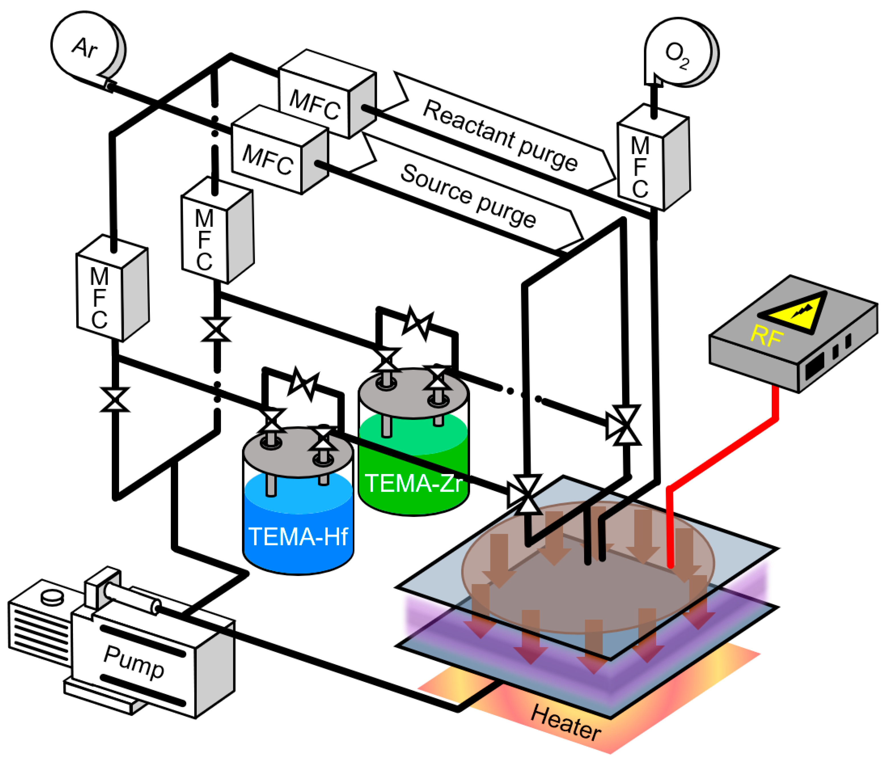
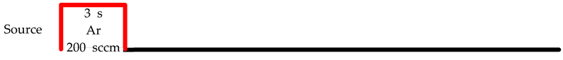
2.1. HZO Thin Film Deposition by PEALD
2.2. Characterization of HZO Thin Films
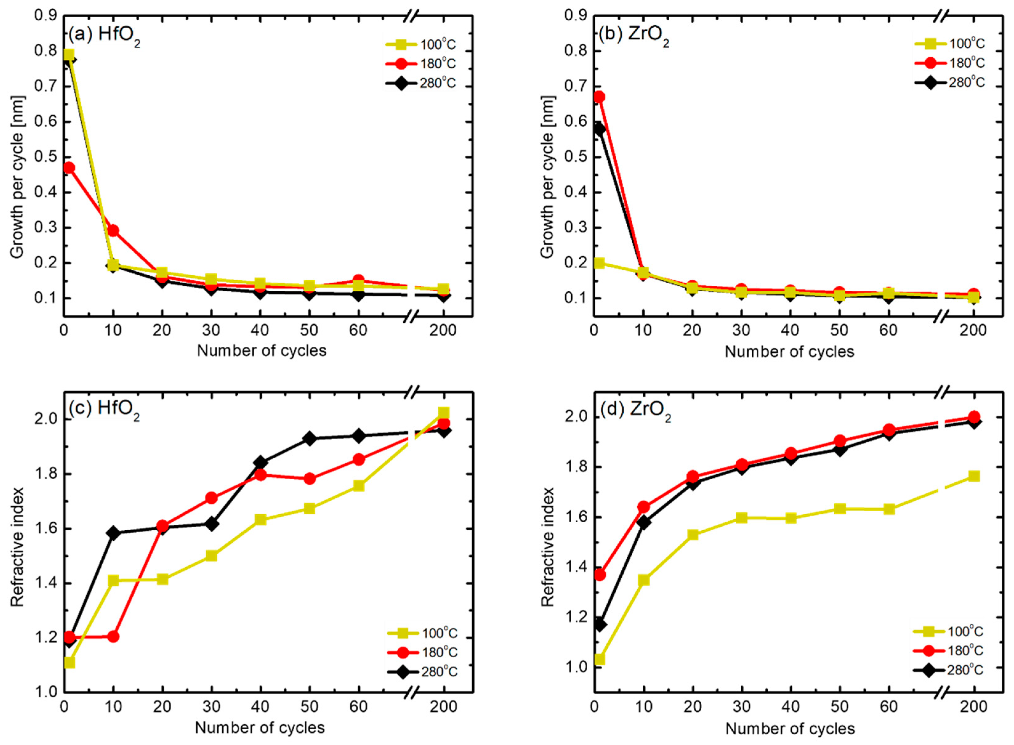
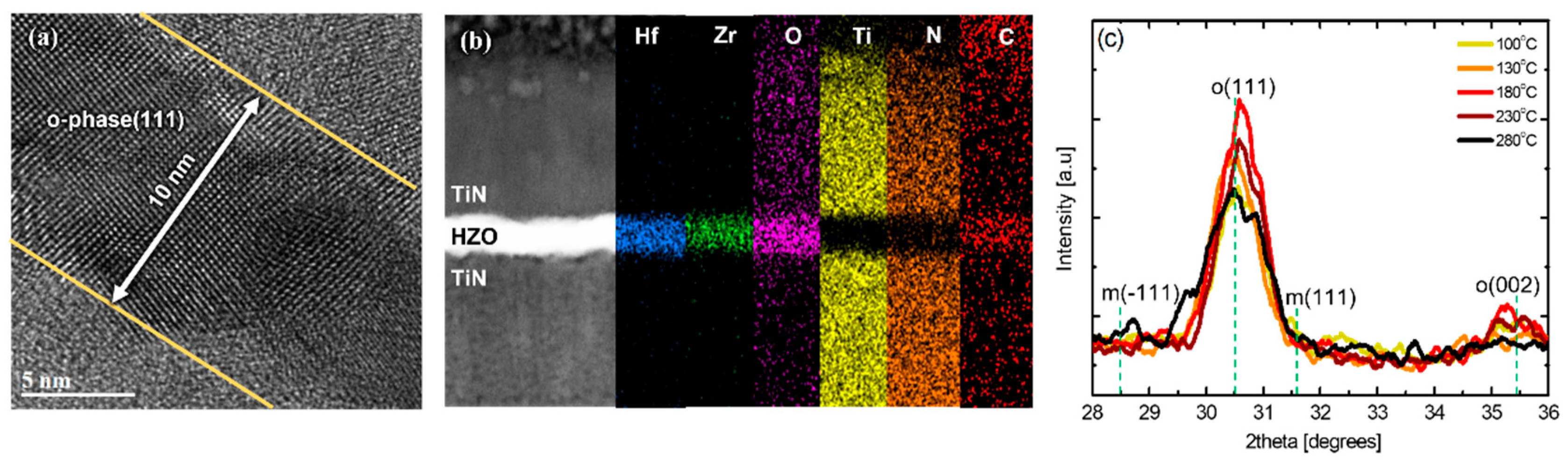
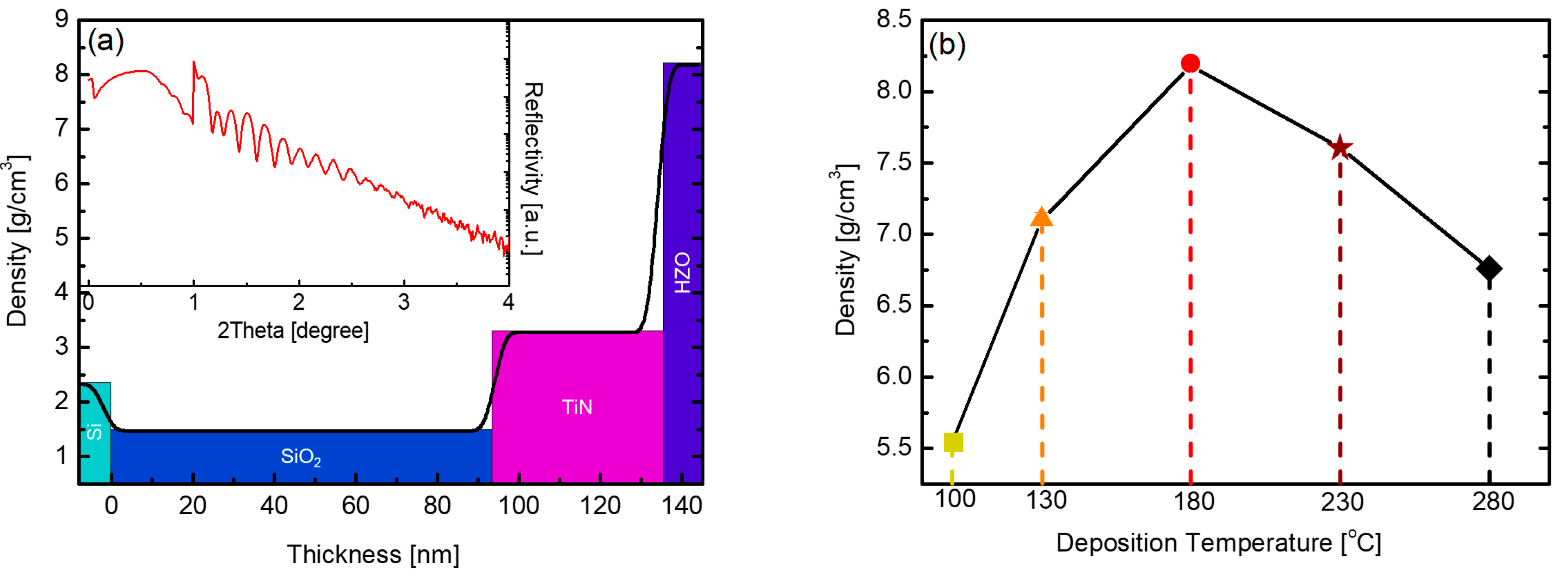
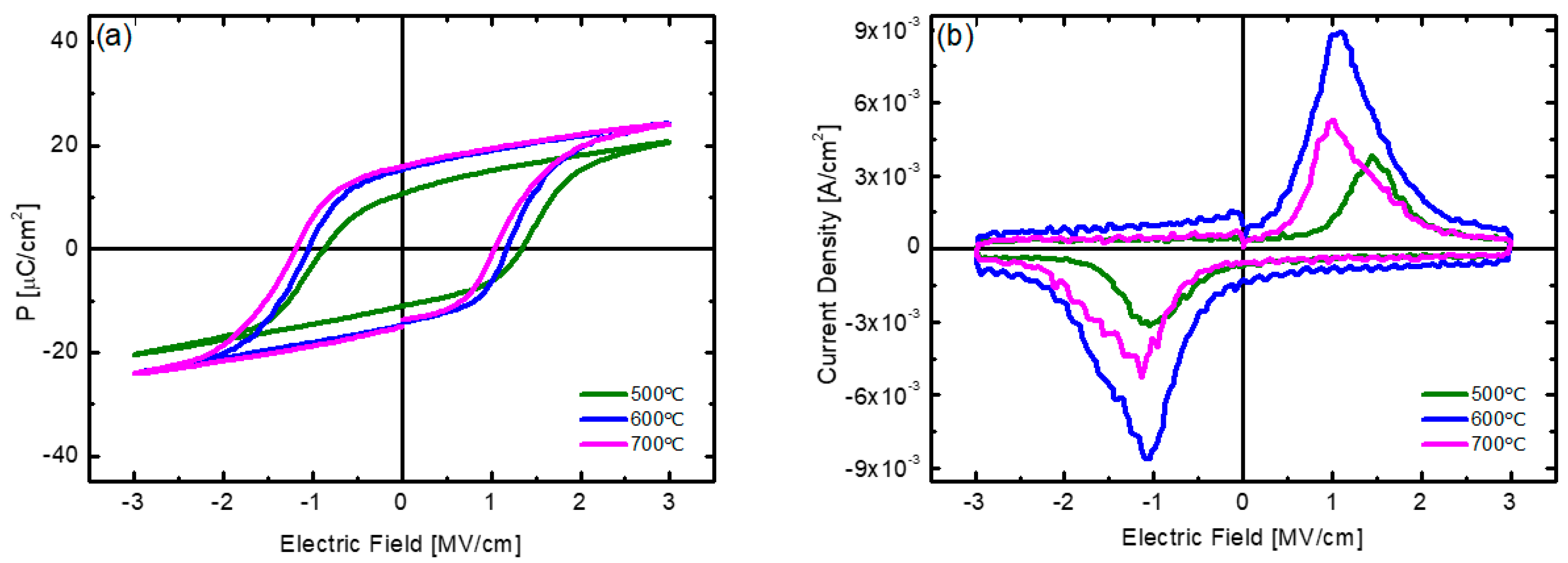
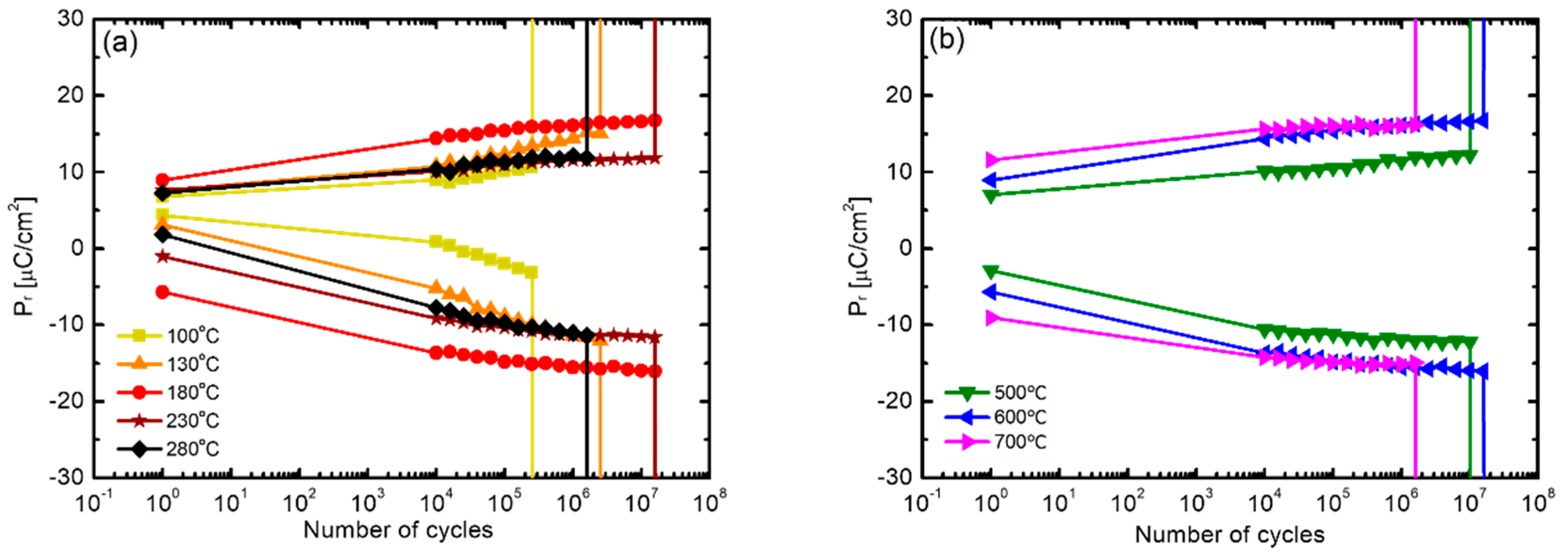
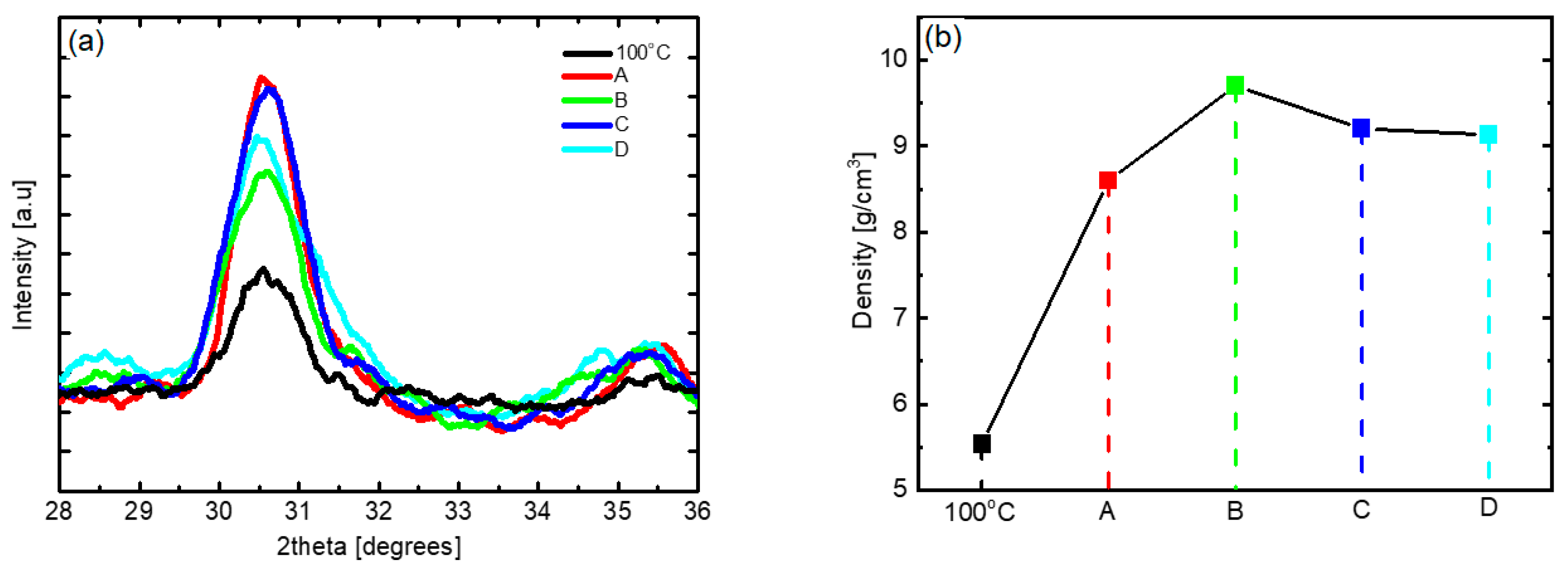
3. Results and Discussion
4. Conclusions
Author Contributions
Funding
Institutional Review Board Statement
Informed Consent Statement
Data Availability Statement
Conflicts of Interest
References
- Böscke, T.S.; Müller, J.; Bräuhaus, D.; Schröder, U.; Böttger, U. Ferroelectricity in Hafnium Oxide Thin Films. Appl. Phys. Lett. 2011, 99, 102903. [Google Scholar] [CrossRef]
- Kim, M.K.; Lee, J.S. Ferroelectric Analog Synaptic Transistors. Nano Lett. 2019, 19, 2044–2050. [Google Scholar] [CrossRef] [PubMed]
- Ni, K.; Sharma, P.; Zhang, J.; Jerry, M.; Smith, J.A.; Tapily, K.; Clark, R.; Mahapatra, S.; Datta, S. Critical Role of Interlayer in Hf0.5Zr0.5O2 Ferroelectric FET Nonvolatile Memory Performance. IEEE Trans. Electron. Devices 2018, 65, 2461–2469. [Google Scholar] [CrossRef]
- Kim, M.K.; Lee, J.S. Synergistic Improvement of Long-Term Plasticity in Photonic Synapses Using Ferroelectric Polarization in Hafnia-Based Oxide-Semiconductor Transistors. Adv. Mater. 2020, 32, e1907826. [Google Scholar] [CrossRef] [PubMed]
- Li, K.-S.; Chen, P.-G.; Lai, T.-Y.; Lin, C.-H.; Cheng, C.-C.; Chen, C.-C.; Wei, Y.-J.; Hou, Y.-F.; Liao, M.-H.; Lee, M.-H. Sub-60mV-Swing Negative-Capacitance FinFET without Hysteresis. In Proceedings of the 2015 IEEE International Electron Devices Meeting (IEDM), Washington, DC, USA, 7–9 December 2015; Volume 4, pp. 22.6.1–22.6.4. [Google Scholar]
- Ambriz-Vargas, F.; Kolhatkar, G.; Broyer, M.; Hadj-Youssef, A.; Nouar, R.; Sarkissian, A.; Thomas, R.; Gomez-Yáñez, C.; Gauthier, M.A.; Ruediger, A. A Complementary Metal Oxide Semiconductor Process-Compatible Ferroelectric Tunnel Junction. ACS Appl. Mater. Interfaces 2017, 9, 13262–13268. [Google Scholar] [CrossRef]
- Nakamura, T.; Nakao, Y.; Kamisawa, A.; Takasu, H. Preparation of Pb(Zr, Ti)O3 Thin Films on Electrodes Including IrO2. Appl. Phys. Lett. 1994, 65, 1522–1524. [Google Scholar] [CrossRef]
- Park, M.H.; Lee, Y.H.; Mikolajick, T.; Schroeder, U.; Hwang, C.S. Review and Perspective on Ferroelectric HfO2-Based Thin Films for Memory Applications. MRS Commun. 2018, 8, 795–808. [Google Scholar] [CrossRef] [Green Version]
- Moazzami, R.; Hu, C.; Shepherd, W.H. Endurance Properties of Ferroelectric PZT Thin Films. In Proceedings of the International Technical Digest on Electron Devices, San Francisco, CA, USA, 9–12 December 1990; pp. 417–420. [Google Scholar]
- Park, M.H.; Lee, Y.H.; Kim, H.J.; Kim, Y.J.; Moon, T.; Do Kim, K.D.; Hyun, S.D.; Mikolajick, T.; Schroeder, U.; Hwang, C.S. Understanding the Formation of the Metastable Ferroelectric Phase in Hafnia–Zirconia Solid Solution Thin Films. Nanoscale 2018, 10, 716–725. [Google Scholar] [CrossRef] [Green Version]
- Cao, R.; Liu, Q.; Liu, M.; Song, B.; Shang, D.; Yang, Y.; Luo, Q.; Wu, S.; Li, Y.; Wang, Y.; et al. Improvement of Endurance in HZO-Based Ferroelectric Capacitor Using Ru Electrode. IEEE Electron. Dev. Lett. 2019, 40, 1744–1747. [Google Scholar] [CrossRef]
- Kim, S.J.; Narayan, D.; Lee, J.-G.; Mohan, J.; Lee, J.S.; Lee, J.; Kim, H.S.; Byun, Y.-C.; Lucero, A.T.; Young, C.D.; et al. Large Ferroelectric Polarization of TiN/Hf0.5Zr0.5O2/TiN Capacitors Due to Stress-Induced Crystallization at Low Thermal Budget. Appl. Phys. Lett. 2017, 111, 242901. [Google Scholar] [CrossRef]
- Kashir, A.; Kim, H.; Oh, S.; Hwang, H. Large Remnant Polarization in a Wake-Up Free Hf0.5Zr0.5O2 Ferroelectric Film through Bulk and Interface Engineering. ACS Appl. Electron. Mater. 2021, 3, 629–638. [Google Scholar] [CrossRef]
- Park, M.H.; Lee, D.H.; Yang, K.; Park, J.-Y.; Yu, G.T.; Park, H.W.; Materano, M.; Mittmann, T.; Lomenzo, P.D.; Mikolajick, T.; et al. Review of Defect Chemistry in Fluorite-Structure Ferroelectrics for Future Electronic Devices. J. Mater. Chem. C 2020, 8, 10526–10550. [Google Scholar] [CrossRef]
- Materlik, R.; Künneth, C.; Kersch, A. The Origin of Ferroelectricity in Hf1−xZrxO2:A Computational Investigation and a Surface Energy Model. J. Appl. Phys. 2015, 117, 134109. [Google Scholar] [CrossRef] [Green Version]
- Hyuk Park, M.; Joon Kim, H.; Jin Kim, Y.; Lee, W.; Moon, T.; Seong Hwang, C. Evolution of Phases and Ferroelectric Properties of Thin Hf0.5Zr0.5O2 Films According to the Thickness and Annealing Temperature. Appl. Phys. Lett. 2013, 102, 242905. [Google Scholar] [CrossRef]
- Saha, A.K.; Grisafe, B.; Datta, S.; Gupta, S.K. Microscopic Crystal Phase Inspired Modeling of Zr Concentration Effects in Hf1−xZrxO2 Thin Films. In Proceedings of the 2019 Symposium on VLSI Technology, Kyoto, Japan, 9–14 June 2019. [Google Scholar]
- Cho, D.-Y.; Jung, H.-S.; Hwang, C.S. Structural Properties and Electronic Structure of HfO2-ZrO2 Composite Films. Phys. Rev. B 2010, 82, 094104. [Google Scholar] [CrossRef]
- Hur, J.; Tasneem, N.; Choe, G.; Wang, P.; Wang, Z.; Khan, A.I.; Yu, S. Direct Comparison of Ferroelectric Properties in Hf0.5Zr0.5O2 between Thermal and Plasma-Enhanced Atomic Layer Deposition. Nanotechnology 2020, 31, 505707. [Google Scholar] [CrossRef] [PubMed]
- Kim, K.M.; Jang, J.S.; Yoon, S.G.; Yun, J.Y.; Chung, N.K. Structural, Optical and Electrical Properties of HfO2 Thin Films Deposited at Low-Temperature Using Plasma-Enhanced Atomic Layer Deposition. Materials 2020, 13, 2008. [Google Scholar] [CrossRef]
- Chen, Z.; Wang, H.; Wang, X.; Chen, P.; Liu, Y.; Zhao, H.; Zhao, Y.; Duan, Y. Low-Temperature Remote Plasma Enhanced Atomic Layer Deposition of ZrO2/Zircone Nanolaminate Film for Efficient Encapsulation of Flexible Organic Light-Emitting Diodes. Sci. Rep. 2017, 7, 40061. [Google Scholar] [CrossRef] [Green Version]
- Xiao, Z.; Kisslinger, K.; Chance, S.; Banks, S. Comparison of Hafnium Dioxide and Zirconium Dioxide Grown by Plasma-Enhanced Atomic Layer Deposition for the Application of Electronic Materials. Crystals. 2020, 10, 136. [Google Scholar] [CrossRef] [Green Version]
- Lin, Y.-H.; Chen, W.-C.; Chen, P.-H.; Lin, C.-Y.; Chang, K.-C.; Chang, Y.-C.; Yeh, C.-H.; Lin, C.-Y.; Jin, F.-Y.; Chen, K.-H.; et al. Effect of Deposition Temperature on Electrical Properties of One-Transistor-One-Capacitor (1T1C) FeRAM Devices. Appl. Phys. Lett. 2020, 117, 023502. [Google Scholar] [CrossRef]
- Myers, T.J.; Throckmorton, J.A.; Borrelli, R.A.; O’Sullivan, M.; Hatwar, T.; George, S.M. Smoothing Surface Roughness Using Al2O3 Atomic Layer Deposition. Appl. Surf. Sci. 2021, 569, 150878. [Google Scholar] [CrossRef]
- Park, T.J.; Kim, J.H.; Jang, J.H.; Kim, U.K.; Lee, S.Y.; Lee, J.; Jung, H.S.; Hwang, C.S. Improved Growth and Electrical Properties of Atomic-Layer-Deposited Metal-Oxide Film by Discrete Feeding Method of Metal Precursor. Chem. Mater. 2011, 23, 1654–1658. [Google Scholar] [CrossRef]
- Groner, M.D.; Fabreguette, F.H.; Elam, J.W.; George, S.M. Low-Temperature Al2O3 Atomic Layer Deposition. Chem. Mater. 2004, 16, 639–645. [Google Scholar] [CrossRef]
- Qi, Y.; Xu, X.; Krylov, I.; Eizenberg, M. Ferroelectricity of as-Deposited HZO Fabricated by Plasma-Enhanced Atomic Layer Deposition at 300°C by Inserting TiO2 Interlayers. Appl. Phys. Lett. 2021, 118, 032906. [Google Scholar] [CrossRef]
- Park, M.H.; Kim, H.J.; Do Kim, K.; Lee, Y.H.; Hyun, S.D.; Hwang, C.S. Impact of Zr Content in Atomic Layer Deposited Hf1−XZrxO2 Thin Films. In Ferroelectricity in Doped Hafnium Oxide: Materials, Properties and Devices; Elsevier: Amsterdam, The Netherlands, 2019; pp. 75–101. [Google Scholar]
- Suzuki, R.; Taoka, N.; Yokoyama, M.; Kim, S.-H.; Hoshii, T.; Maeda, T.; Yasuda, T.; Ichikawa, O.; Fukuhara, N.; Hata, M.; et al. Impact of Atomic Layer Deposition Temperature on HfO2/InGaAs Metal-Oxide-Semiconductor Interface Properties. J. Appl. Phys. 2012, 112, 084103. [Google Scholar] [CrossRef]
- Kim, K.D.; Lee, Y.H.; Gwon, T.; Kim, Y.J.; Kim, H.J.; Moon, T.; Hyun, S.D.; Park, H.W.; Park, M.H.; Hwang, C.S. Scale-Up and Optimization of HfO2-ZrO2 Solid Solution Thin Films for the Electrostatic Supercapacitors. Nano Energy 2017, 39, 390–399. [Google Scholar] [CrossRef]
- Kisi, E.H.; Howard, C.J.; Hill, R.J. Crystal Structure of Orthorhombic Zirconia in Partially Stabilized Zirconia. J. Am. Ceram. Soc. 1989, 72, 1757–1760. [Google Scholar] [CrossRef]
- Lim, J.-W.; Park, J.-S.; Kang, S.-W. Kinetic Modeling of Film Growth Rates of TiN Films in Atomic Layer Deposition. J. Appl. Phys. 2000, 87, 4632–4634. [Google Scholar] [CrossRef]
- Jaffe, J.E.; Bachorz, R.A.; Gutowski, M. Low-Temperature Polymorphs of ZrO2 and HfO2:A Density-Functional Theory Study. Phys. Rev. B 2005, 72, 144107. [Google Scholar] [CrossRef]
- Lowther, J.E.; Dewhurst, J.K.; Leger, J.M.; Haines, J. Relative Stability of ZrO2 and HfO2 Structural Phases. Phys. Rev. B 1999, 60, 14485–14488. [Google Scholar] [CrossRef]
- Haggerty, R.P.; Sarin, P.; Apostolov, Z.D.; Driemeyer, P.E.; Kriven, W.M. Thermal Expansion of HfO2 and ZrO2. J. Am. Ceram. Soc. 2014, 97, 2213–2222. [Google Scholar] [CrossRef]
- Lin, Y.-C.; McGuire, F.; Franklin, A.D. Realizing Ferroelectric Hf0.5Zr0.5O2 with Elemental Capping Layers. J. Vac. Sci. Technol. B Nanotechnol. Microelectron. Mater. Process. Meas. Phenom. 2018, 36, 011204. [Google Scholar] [CrossRef]
- Goh, Y.; Jeon, S. First-Order Reversal Curve Diagrams for Characterizing Ferroelectricity of Hf0.5Zr0.5O2 Films Grown at Different Rates. J. Vac. Sci. Technol. B Nanotechnol. Microelectron. Mater. Process. Meas. Phenom. 2018, 36, 052204. [Google Scholar] [CrossRef]
- Chen, W.-C.; Tan, Y.-F.; Lin, S.-K.; Zhang, Y.-C.; Chang, K.-C.; Lin, Y.-H.; Yeh, C.-H.; Wu, C.-W.; Yeh, Y.-H.; Wang, K.-Y.; et al. Performance Improvement by Modifying Deposition Temperature in HfZrOx Ferroelectric Memory. IEEE Trans. Electron. Devices 2021, 68, 3838–3842. [Google Scholar] [CrossRef]
- Pešić, M.; Fengler, F.P.G.; Larcher, L.; Padovani, A.; Schenk, T.; Grimley, E.D.; Sang, X.; LeBeau, J.M.; Slesazeck, S.; Schroeder, U.; et al. Physical Mechanisms behind the Field-Cycling Behavior of HfO2-Based Ferroelectric Capacitors. Adv. Funct. Mater. 2016, 26, 4601–4612. [Google Scholar] [CrossRef]
- Goh, Y.; Cho, S.H.; Park, S.-H.K.; Jeon, S. Oxygen Vacancy Control as a Strategy to Achieve Highly Reliable Hafnia Ferroelectrics Using Oxide Electrode. Nanoscale 2020, 12, 9024–9031. [Google Scholar] [CrossRef] [PubMed]
- Kim, S.J.; Mohan, J.; Lee, J.; Lee, J.S.; Lucero, A.T.; Young, C.D.; Colombo, L.; Summerfelt, S.R.; San, T.; Kim, J. Effect of Film Thickness on the Ferroelectric and Dielectric Properties of Low-Temperature (400 °C) Hf0.5Zr0.5O2 Films. Appl. Phys. Lett. 2018, 112, 172902. [Google Scholar] [CrossRef]
- Kim, S.J.; Mohan, J.; Summerfelt, S.R.; Kim, J. Ferroelectric Hf0.5Zr0.5O2 Thin Films: A Review of Recent Advances. JOM 2019, 71, 246–255. [Google Scholar] [CrossRef]
- Jiang, P.; Luo, Q.; Xu, X.; Gong, T.; Yuan, P.; Wang, Y.; Gao, Z.; Wei, W.; Tai, L.; Lv, H. Wake-up Effect in HfO2-Based Ferroelectric Films. Adv. Electron. Mater. 2021, 7, 2000728. [Google Scholar] [CrossRef]
- Kashir, A.; Oh, S.; Hwang, H. Defect Engineering for Control of Wake-Up Effect in HfO2-Based Ferroelectrics. arXiv 2020, arXiv:2009.04714. [Google Scholar]
- Shekhawat, A.; Walters, G.; Chung, C.-C.; Garcia, R.; Liu, Y.; Jones, J.; Nishida, T.; Moghaddam, S. Effect of Forming Gas Furnace Annealing on the Ferroelectricity and Wake-Up Effect of Hf0.5Zr0.5O2 Thin Films. ECS J. Solid State Sci. Technol. 2020, 9, 024011. [Google Scholar] [CrossRef]
- Kim, H.J.; Park, M.H.; Kim, Y.J.; Lee, Y.H.; Moon, T.; Do Kim, K.D.; Hyun, S.D.; Hwang, C.S. A Study on the Wake-Up Effect of Ferroelectric Hf0.5Zr0.5O2 Films by Pulse-Switching Measurement. Nanoscale 2016, 8, 1383–1389. [Google Scholar] [CrossRef] [PubMed]
- Knoops, H.C.M.; Faraz, T.; Arts, K.; Kessels, W.M.M. Status and Prospects of Plasma-Assisted Atomic Layer Deposition. J. Vac. Sci. Technol. A 2019, 37, 030902. [Google Scholar] [CrossRef] [Green Version]
- Deng, Z.; He, W.; Duan, C.; Shan, B.; Chen, R. Atomic Layer Deposition Process Optimization by Computational Fluid Dynamics. Vacuum 2016, 123, 103–110. [Google Scholar] [CrossRef]
- Leys, M.R.; Veenvliet, H. A Study of the Growth Mechanism of Epitaxial GaAs as Grown by the Technique of Metal Organic Vapour Phase Epitaxy. J. Cryst. Growth. 1981, 55, 145–153. [Google Scholar] [CrossRef]


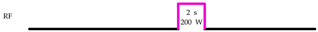
| Deposition Temperature Maintenance Gas Flow Pressure | 100−280 °C 600 sccm 1.3 Torr |
|---|---|
 | |
 | |
 | |
 | |
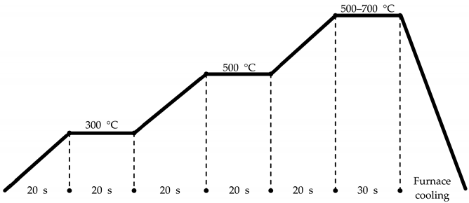
| Annealing Temperature Ambient Pressure | 500−700 °C N2 Atmosphere 5 Torr |
|---|---|
 | |
| Ref. | Growth Method | Electrode | Deposition Temperature | Annealing Temperature | 2Pr (μC/cm2) | Fatigue Endurance (Number of Cycles) |
|---|---|---|---|---|---|---|
| Our work | PEALD | TiN | 180 °C | 600 °C | 38.2 | 1.6 × 10⁷ |
| [19] | PEALD | TiN | 250 °C | 450 °C | 35 | 1.6 × 10⁵ |
| [10] | THALD | TiN | 280 °C | 600 °C | 29 | − |
| [11] | THALD | Ru | 280 °C | 500 °C | 36 | 1.2 × 10¹¹ |
| [12] | THALD | TiN | 250 °C | 400 °C | 48 | − |
| [13] | THALD | W | 250 °C | 720 °C | 42 | 1 × 10⁴ |
Publisher’s Note: MDPI stays neutral with regard to jurisdictional claims in published maps and institutional affiliations. |
© 2022 by the authors. Licensee MDPI, Basel, Switzerland. This article is an open access article distributed under the terms and conditions of the Creative Commons Attribution (CC BY) license (https://creativecommons.org/licenses/by/4.0/).
Share and Cite
Kim, H.-G.; Hong, D.-H.; Yoo, J.-H.; Lee, H.-C. Effect of Process Temperature on Density and Electrical Characteristics of Hf0.5Zr0.5O2 Thin Films Prepared by Plasma-Enhanced Atomic Layer Deposition. Nanomaterials 2022, 12, 548. https://doi.org/10.3390/nano12030548
Kim H-G, Hong D-H, Yoo J-H, Lee H-C. Effect of Process Temperature on Density and Electrical Characteristics of Hf0.5Zr0.5O2 Thin Films Prepared by Plasma-Enhanced Atomic Layer Deposition. Nanomaterials. 2022; 12(3):548. https://doi.org/10.3390/nano12030548
Chicago/Turabian StyleKim, Hak-Gyeong, Da-Hee Hong, Jae-Hoon Yoo, and Hee-Chul Lee. 2022. "Effect of Process Temperature on Density and Electrical Characteristics of Hf0.5Zr0.5O2 Thin Films Prepared by Plasma-Enhanced Atomic Layer Deposition" Nanomaterials 12, no. 3: 548. https://doi.org/10.3390/nano12030548
APA StyleKim, H.-G., Hong, D.-H., Yoo, J.-H., & Lee, H.-C. (2022). Effect of Process Temperature on Density and Electrical Characteristics of Hf0.5Zr0.5O2 Thin Films Prepared by Plasma-Enhanced Atomic Layer Deposition. Nanomaterials, 12(3), 548. https://doi.org/10.3390/nano12030548