
Non-Restoring Array Divider Using Optimized CAS Cells Based on Quantum-Dot Cellular Automata with Minimized Latency and Power Dissipation for Quantum Computing


Abstract
:1. Introduction
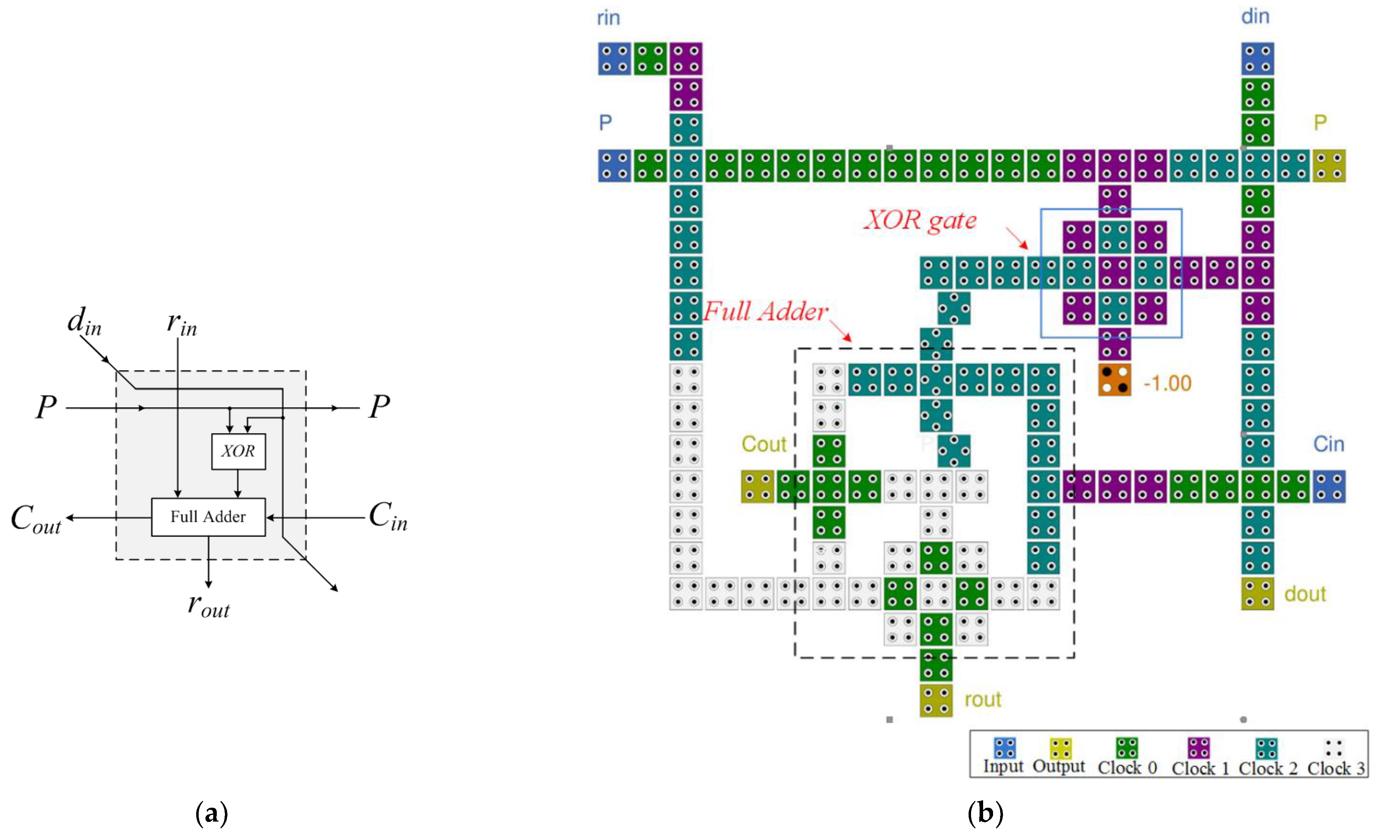
- We propose a full adder with minimized area and latency. Using this, a controlled add/subtract (CAS) cell and divider are proposed.
- Through operation analysis and comparison through circuit simulation, the delay time, which is the most important consideration in mid-to-large circuit designs such as dividers, is optimized.
- The energy loss of the entire structure is minimized by minimizing the energy dissipation of the full adder, which is the main operation structure of the divider.
2. Related Works
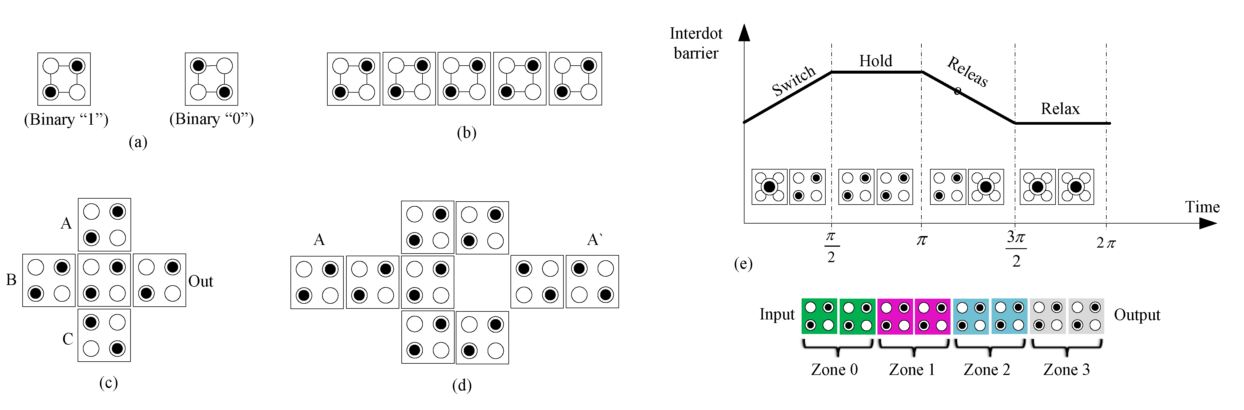
2.1. Basic QCA
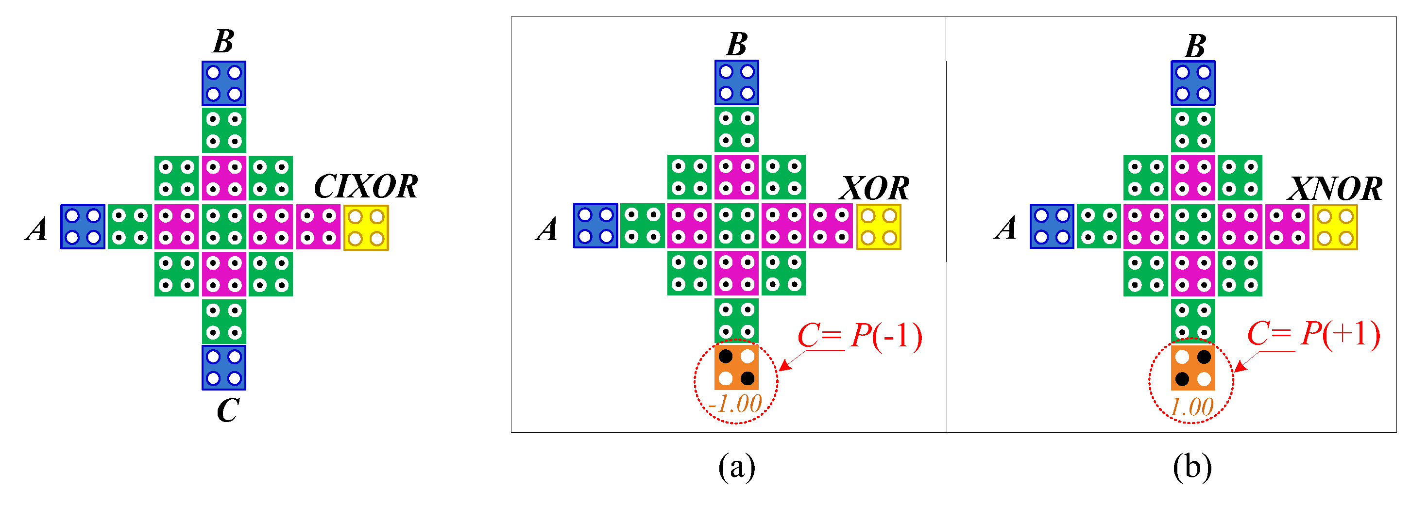
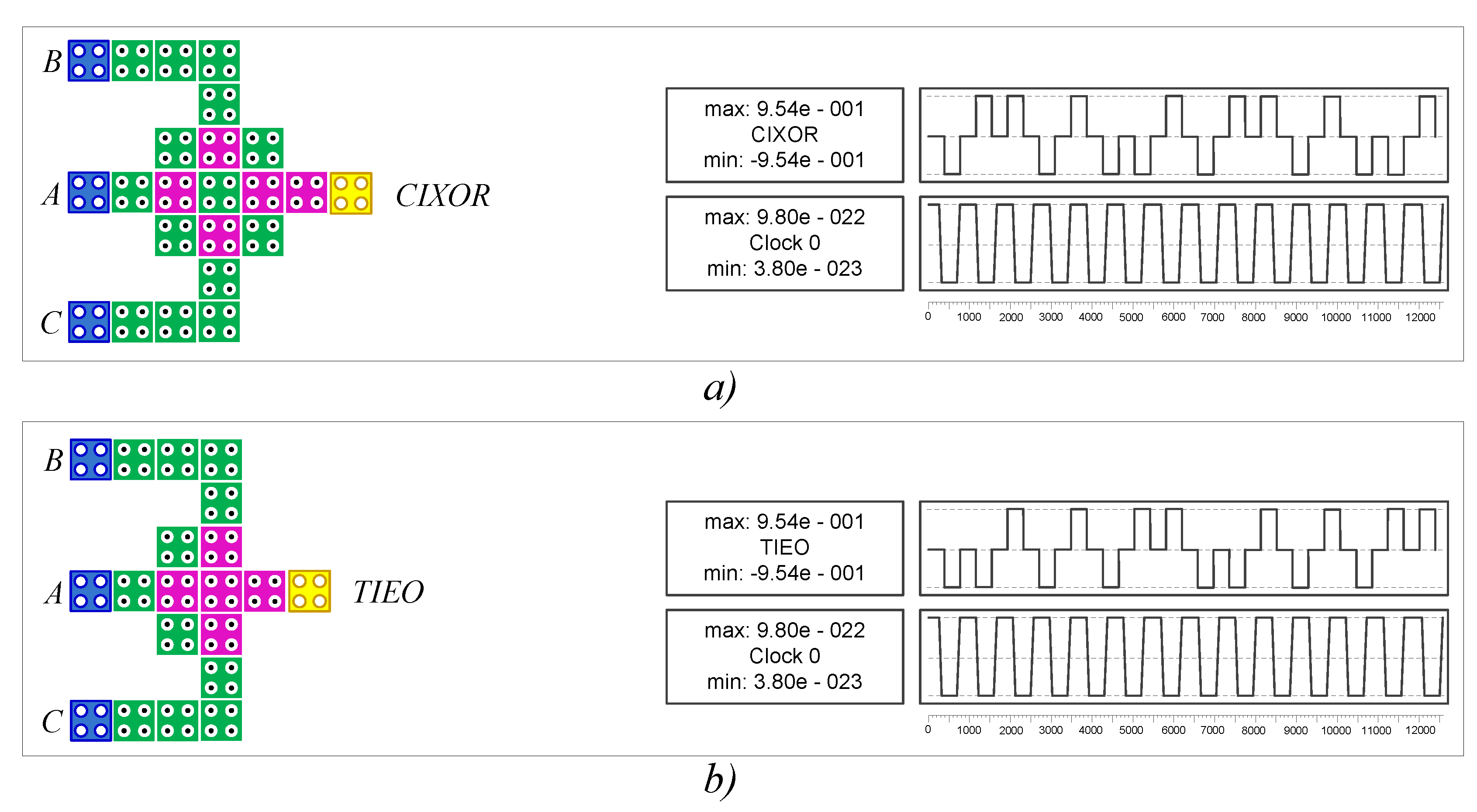
2.2. Cell Interaction XOR Gate
2.3. Non-Restoring Array Divider
3. Proposed Structures
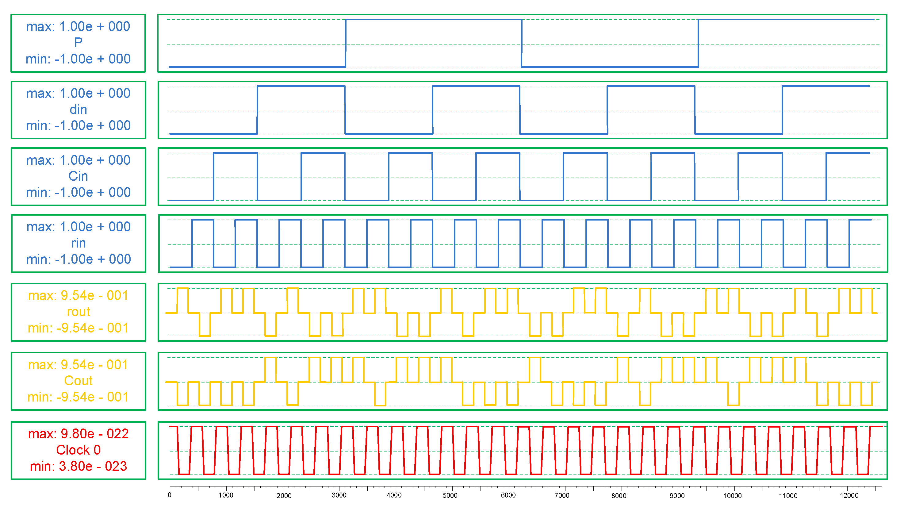
3.1. Proposed CAS Cell
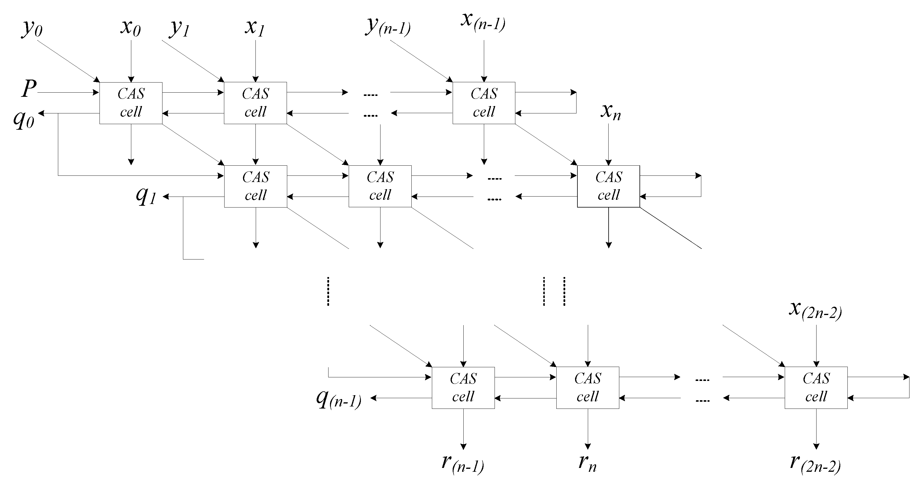
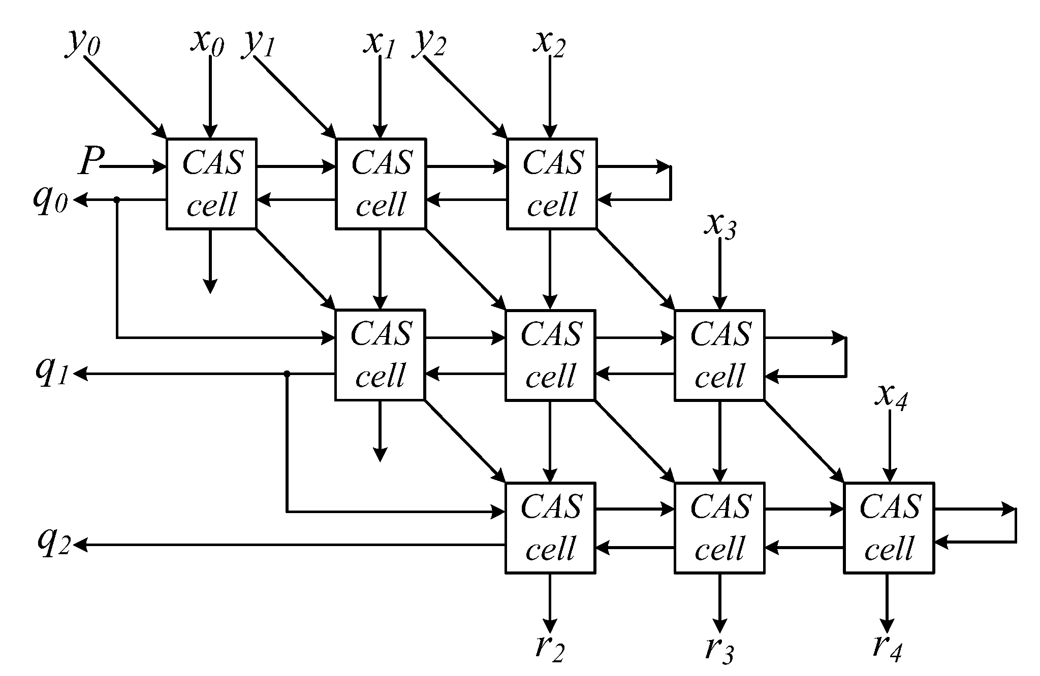
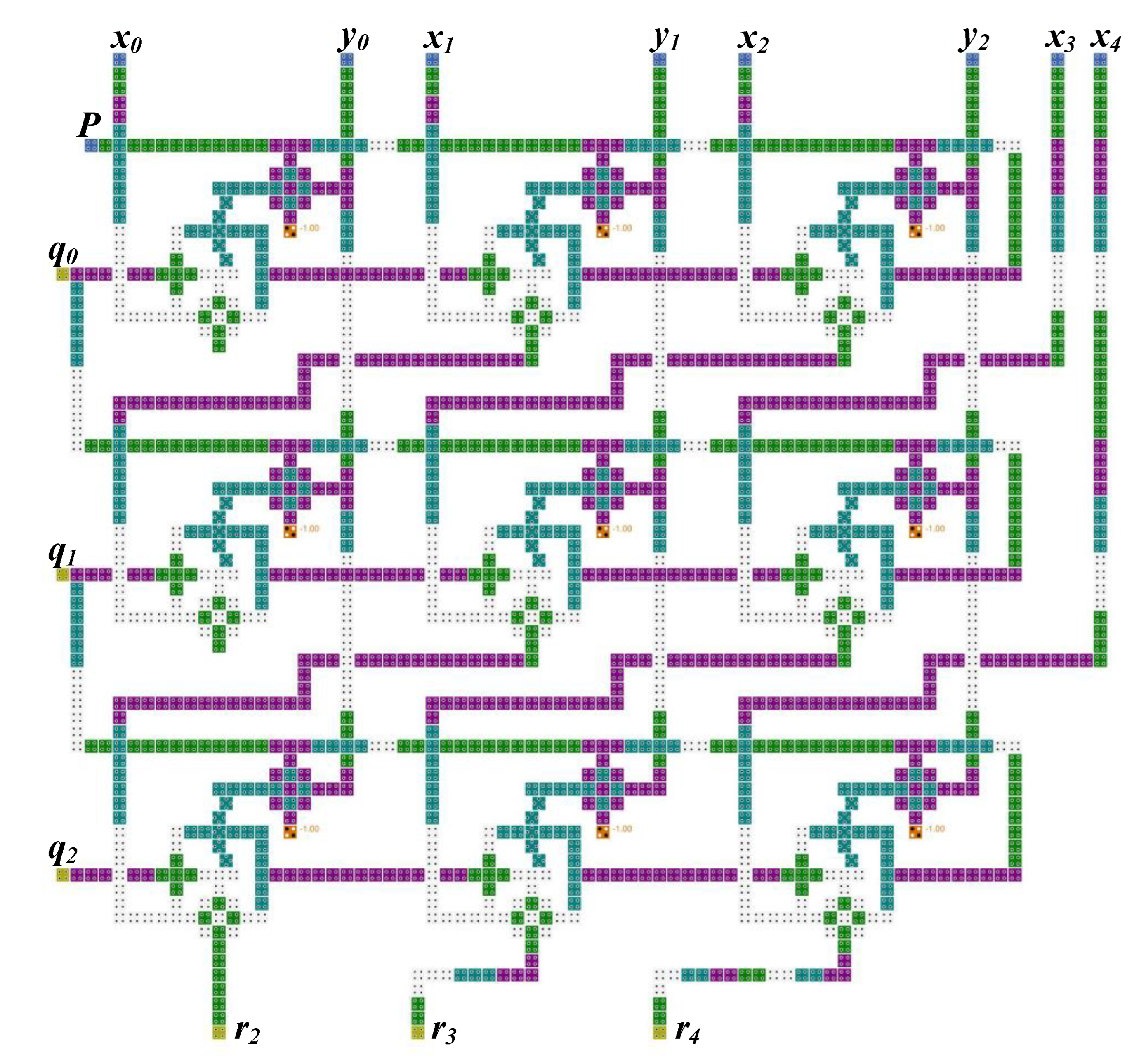
3.2. Design and Implementation of N-RAD
4. Discussion
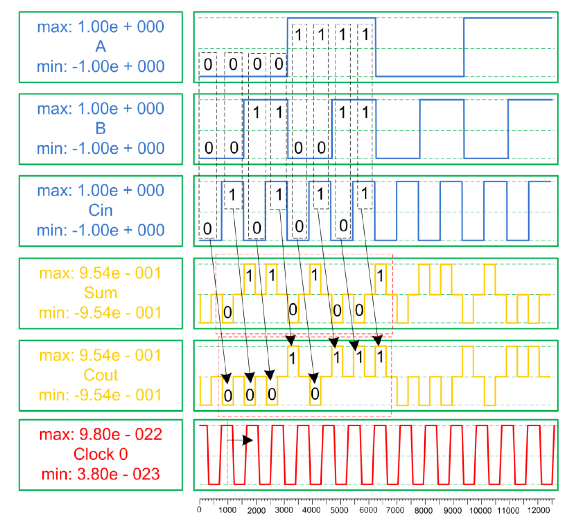
4.1. Structural Analysis
4.2. Power Dissipation Analysis
5. Conclusions
Author Contributions
Funding
Data Availability Statement
Conflicts of Interest
References
- Campano, R. Technology Roadmap for Nanoelectronics; European Commission IST Program: Brussels, Belgium, 2000. [Google Scholar]
- Lent, C.S.; Tougaw, P.D.; Porod, W.; Bernstein, G.H. Quantum cellular automata. Nanotechnology 1993, 4, 49–57. [Google Scholar] [CrossRef]
- Safoev, N.; Jeon, J.C. A novel controllable inverter and adder/subtractor in quantum-dot cellular automata using cell interaction based XOR gate. Microelectron. Eng. 2020, 222, 111197. [Google Scholar] [CrossRef]
- Jeon, J.C. 7-input majority gate based priority encoder using multi-layer quantum-dot cellular automata. Adv. Sci. Lett. 2017, 23, 10118–10122. [Google Scholar] [CrossRef]
- Cho, H.; Swartzlander, E.E. Adder designs and analyses for quantum-dot cellular automata. IEEE Trans. Nanotechnol. 2007, 6, 374–383. [Google Scholar] [CrossRef]
- Seyedi, S.; Navimpipour, N.J. An efficient structure for designing a nano-scale fault-tolerant 2:1 multiplexer based on quantum-dot cellular automata. Optik 2022, 251, 168409. [Google Scholar] [CrossRef]
- Seyedi, S.; Navimpipour, N.J. Designing a three-level full-adder based on nano-scale quantum dot cellular automata. Photonic Netw. Commun. 2021, 42, 184–193. [Google Scholar] [CrossRef]
- Seyedi, S.; Navimpipour, N.J. Ultra-efficient adders and even parity generators in nano scale. Comput. Electr. Eng. 2021, 96, 107548. [Google Scholar]
- Noorallahzadeh, M.; Mosleh, M.; Seyedi, S. Efficient Designs of Reversible Synchronous Counters in Nanoscale. Circuits Syst. Signal Process. 2021, 40, 5367–5380. [Google Scholar] [CrossRef]
- Makanda, K.; Jeon, J.C. Combinational Circuit Design Based on Quantum-Dot Cellular Automata. Int. J. Control Autom. 2014, 7, 369–378. [Google Scholar] [CrossRef]
- Obermann, S.F.; Flynn, M.J. Division algorithms and implementations. IEEE Trans. Comput. 1997, 46, 833–854. [Google Scholar] [CrossRef] [Green Version]
- Ahmad, F.; Bhat, G.M.; Khademolhosseini, H.; Azimi, S.; Angizi, S.; Navi, K. Towards single layer quantum-dot cellular automata adders based on explicit interaction of cells. J. Comput. Sci. 2016, 16, 8–15. [Google Scholar] [CrossRef]
- Safoev, N.; Jeon, J.C. Design and Evaluation of Cell Interaction Based Vedic Multiplier Using Quantum-Dot Cellular Automata. Electronics 2020, 9, 1036. [Google Scholar] [CrossRef]
- Safoev, N.; Jeon, J.C. Design of high-performance QCA incrementer/decrementer circuit based on adder/subtractor methodology. Microprocess. Microsyst. 2020, 72, 102927. [Google Scholar] [CrossRef]
- Erniyazov, S.; Jeon, J.C. Carry save adder and carry look ahead adder using inverter chain based coplanar QCA full adder for low energy dissipation. Microelectron. Eng. 2019, 211, 37–43. [Google Scholar] [CrossRef]
- Parhami, B. Computer Arithmetic Algorithms and Hardware Designs; Oxford University Press: New York, NY, USA, 2010. [Google Scholar]
- Cui, H.; Cai, L.; Yang, X.; Feng, C.; Qin, T. Design of nonrestoring binary array divider in quantum-dot cellular automata. Micro Nano Lett. 2014, 9, 464–467. [Google Scholar] [CrossRef]
- Sayedsalehi, S.; Azghadi, M.R.; Angizi, S.; Navi, K. Restoring and non-restoring array divider designs in quantum-dot cellular automata. Inf. Sci. 2015, 311, 86–101. [Google Scholar] [CrossRef]
- Mohammadi, M.; Gorgin, S.; Mohammadi, M. Design of non-restoring divider in quantum-dot cellular automata technology. IET Circuits Devices Syst. 2017, 11, 135–141. [Google Scholar] [CrossRef] [Green Version]
- Sasamal, T.N.; Singh, A.K.; Ghanekar, U. Design of non-restoring binary array divider in majority logic-based QCA. Electron. Lett. 2016, 52, 2001–2003. [Google Scholar] [CrossRef]
- Almatrood, A.F.; Singh, H. QCA circuit design of n-bit non-restoring binary array divider. J. Eng. 2018, 2018, 348–353. [Google Scholar] [CrossRef]
- Walus, K.; Dysart, T.J.; Jullien, G.A.; Budiman, R.A. QCADesigner: A rapid design and simulation tool for quantum-dot cellular automata. IEEE Trans. Nanotechnol. 2004, 3, 26–31. [Google Scholar] [CrossRef]
- Jeon, J.C. Low Complexity QCA Universal Shift Register Design Using Multiplexer and D Flip-Flop Based on Electronic Correlations. J. Supercomput. 2019, 76, 6438–6452. [Google Scholar] [CrossRef]
- Seyedi, S.; Navimipour, N.J. Design and evaluation of a new structure for fault-tolerance full-adder based on quantum-dot cellular automata. Nano Commun. Netw. 2018, 16, 1–9. [Google Scholar] [CrossRef]
- Sherizadeh, R.; Navimipour, N.J. Designing a 2-to-4 decoder on nanoscale based on quantum-dot cellular automata for energy dissipation improving. Optik-Int. J. Light Electron Opt. 2018, 158, 477–489. [Google Scholar] [CrossRef]
- Seyedi, S.; Navimipour, N.J. An Optimized Three-Level Design of Decoder Based on Nanoscale Quantum-Dot Cellular Automata. Int. J. Theor. Phys. 2018, 57, 2022–2033. [Google Scholar] [CrossRef]
- Liu, W.; Lu, L.; O’Neill, M.; Swartzlander, E.E., Jr. A First Step toward Cost Functions for Quantum-Dot Cellular Automata Designs. IEEE Trans. Nanotechnol. 2014, 13, 476–487. [Google Scholar]
- Kumar, D.; Mitra, D. Design of a practical fault-tolerant adder in QCA. Microelectron. J. 2016, 53, 90–104. [Google Scholar] [CrossRef]
- Bhoi, B.; Misra, N.K.; Lafifa, J.; Pradhan, M. Low-cost synthesis approach for reversible authenticator circuits in QCA environment. Int. J. Nanoelectron. Mater. 2019, 12, 205–220. [Google Scholar]
- Safoev, N. Circuit Design for Arithmetic Operations Based on the Quantum-Dot Cellular Automata Using Cell Interaction XOR Gates. Master’s Thesis, Kumoh National Institute of Technology, Gumi, Korea, 2018. [Google Scholar]
- Angizi, S.; Alkaldy, E.; Bagherzadeh, N.; Navi, K. Novel robust single layer wire crossing approach for exclusive or sum of products logic design with quantum-dot cellular automata. J. Low Power Electron. 2014, 10, 259–271. [Google Scholar] [CrossRef]
- Mohammadyan, S.; Angizi, S.; Navi, K. New fully single layer QCA full-adder cell based on feedback model. Int. J. High Perform. Syst. Archit. 2015, 5, 202–208. [Google Scholar] [CrossRef]
- Abedi, D.; Jaberipur, G.; Sangsefidi, M. Coplanar full adder in quantum-dot cellular automata via clock-zone-based crossover. IEEE Trans. Nanotechnol. 2015, 14, 497–504. [Google Scholar] [CrossRef]
- Labrado, C.; Thapliyal, H. Design of adder and subtractor circuits in majority logic-based field-coupled QCA nanocomputing. Electron. Lett. 2016, 52, 464–466. [Google Scholar] [CrossRef]
- Srivastava, S.; Asthana, A.; Bhanja, S.; Sarkar, S. QCAPro-an error power estimation tool for QCA circuit design. In Proceedings of the IEEE International Symposium Circuits and Systems, Rio de Janeiro, Brazil, 15–18 May 2011; pp. 2377–2380. [Google Scholar]


| Parameters | Bistable Approximation | Coherence Vector |
|---|---|---|
| Cell size (nm) | 18 | 18 |
| Dot diameter (nm) | 5 | 5 |
| Cell separation (nm) | 2 | 2 |
| Layer separation (nm) | 11.5 | 11.5 |
| Clock high (J) | 9.8 × 10⁻²² | 9.8 × 10⁻²² |
| Clock low (J) | 3.8 × 10⁻²³ | 3.8 × 10⁻²³ |
| Clock shift | 0 | 0 |
| Clock amplitude factor | 2.0 | 2.0 |
| Relative permittivity | 12.9 | 12.9 |
| Radius of effect (nm) | 65 | 80 |
| Number of samples | 50,000 | - |
| Convergence tolerance | 0.001 | - |
| Max. iterations per sample | 100 | - |
| Temperature (K) | - | 1 |
| Total simulation time (s) | - | 7 × 10⁻¹¹ |
| Circuit | Cell Count | Total Area (Μm2) | Latency (Clock Cycle) | Condition |
|---|---|---|---|---|
| TIEO gate [12] | 14 | 0.02 | 0.50 | Normal |
| CIXOR gate | 17 | 0.02 | 0.50 | Robust |
| Circuit | Cell Count | Total Area (μm2) | Latency (Clock Cycle) | Crossover | AT2 |
|---|---|---|---|---|---|
| [17] | 111 | 0.20 | 1.25 | Coplanar | 0.312500 |
| [18] | 94 | 0.14 | 0.75 | Multilayer | 0.078750 |
| [19] | 58 | 0.03 | 0.75 | Multilayer | 0.016875 |
| [20] | 43 | 0.05 | 0.75 | Coplanar | 0.028125 |
| [21] | 62 | 0.05 | 0.70 | Multilayer | 0.024500 |
| [12] | 41 | 0.06 | 0.50 | Coplanar | 0.015000 |
| Proposed | 42 | 0.05 | 0.50 | Coplanar | 0.012500 |
| Circuit | Cell Count | Total Area (μm2) | Latency(Clock Cycle) | Structure |
|---|---|---|---|---|
| [17] | 3742 | 6.20 | 26.25 | Coplanar |
| [20] | 1686 | 3.34 | 6.75 | Coplanar |
| [19] | 1852 | 1.92 | 7.50 | Multilayer |
| [21] | 1436 | 1.53 | 5.75 | Multilayer |
| The proposed | 1489 | 2.10 | 5.50 | Coplanar |
| Circuit | Avg. Leakage Energy Dissipation (meV) | Avg. Switching Energy Dissipation (meV) | Avg. Energy Dissipation of Circuit (meV) | ||||||
|---|---|---|---|---|---|---|---|---|---|
| 0.5Ek | 1.0Ek | 1.5Ek | 0.5Ek | 1.0Ek | 1.5Ek | 0.5Ek | 1.0Ek | 1.5Ek | |
| [17] | 48.69 | 150.52 | 270.62 | 269.26 | 233.79 | 199.82 | 317.95 | 384.31 | 470.44 |
| [31] | 27.69 | 84.08 | 151.39 | 159.68 | 140.88 | 122.21 | 187.37 | 224.96 | 273.60 |
| [32] | 27.91 | 85.42 | 153.58 | 147.67 | 127.78 | 108.61 | 175.58 | 213.20 | 262.19 |
| [33] | 40.07 | 118.85 | 208.7 | 181.61 | 153.67 | 128.82 | 221.68 | 272.52 | 337.53 |
| [34] | 37.21 | 98.5 | 165.04 | 61.97 | 50.90 | 42.31 | 99.19 | 149.40 | 207.34 |
| Proposed | 22.71 | 62.93 | 107.72 | 62.60 | 52.94 | 44.42 | 85.31 | 115.87 | 152.13 |
Publisher’s Note: MDPI stays neutral with regard to jurisdictional claims in published maps and institutional affiliations. |
© 2022 by the authors. Licensee MDPI, Basel, Switzerland. This article is an open access article distributed under the terms and conditions of the Creative Commons Attribution (CC BY) license (https://creativecommons.org/licenses/by/4.0/).
Share and Cite
Kim, H.-I.; Jeon, J.-C. Non-Restoring Array Divider Using Optimized CAS Cells Based on Quantum-Dot Cellular Automata with Minimized Latency and Power Dissipation for Quantum Computing. Nanomaterials 2022, 12, 540. https://doi.org/10.3390/nano12030540
Kim H-I, Jeon J-C. Non-Restoring Array Divider Using Optimized CAS Cells Based on Quantum-Dot Cellular Automata with Minimized Latency and Power Dissipation for Quantum Computing. Nanomaterials. 2022; 12(3):540. https://doi.org/10.3390/nano12030540
Chicago/Turabian StyleKim, Hyun-Il, and Jun-Cheol Jeon. 2022. "Non-Restoring Array Divider Using Optimized CAS Cells Based on Quantum-Dot Cellular Automata with Minimized Latency and Power Dissipation for Quantum Computing" Nanomaterials 12, no. 3: 540. https://doi.org/10.3390/nano12030540
APA StyleKim, H.-I., & Jeon, J.-C. (2022). Non-Restoring Array Divider Using Optimized CAS Cells Based on Quantum-Dot Cellular Automata with Minimized Latency and Power Dissipation for Quantum Computing. Nanomaterials, 12(3), 540. https://doi.org/10.3390/nano12030540