
Synergy of Electrostatic and Chemical Doping to Improve the Performance of Junctionless Carbon Nanotube Tunneling Field-Effect Transistors: Ultrascaling, Energy-Efficiency, and High Switching Performance

 ,
,  ,
, 


Abstract
:1. Introduction
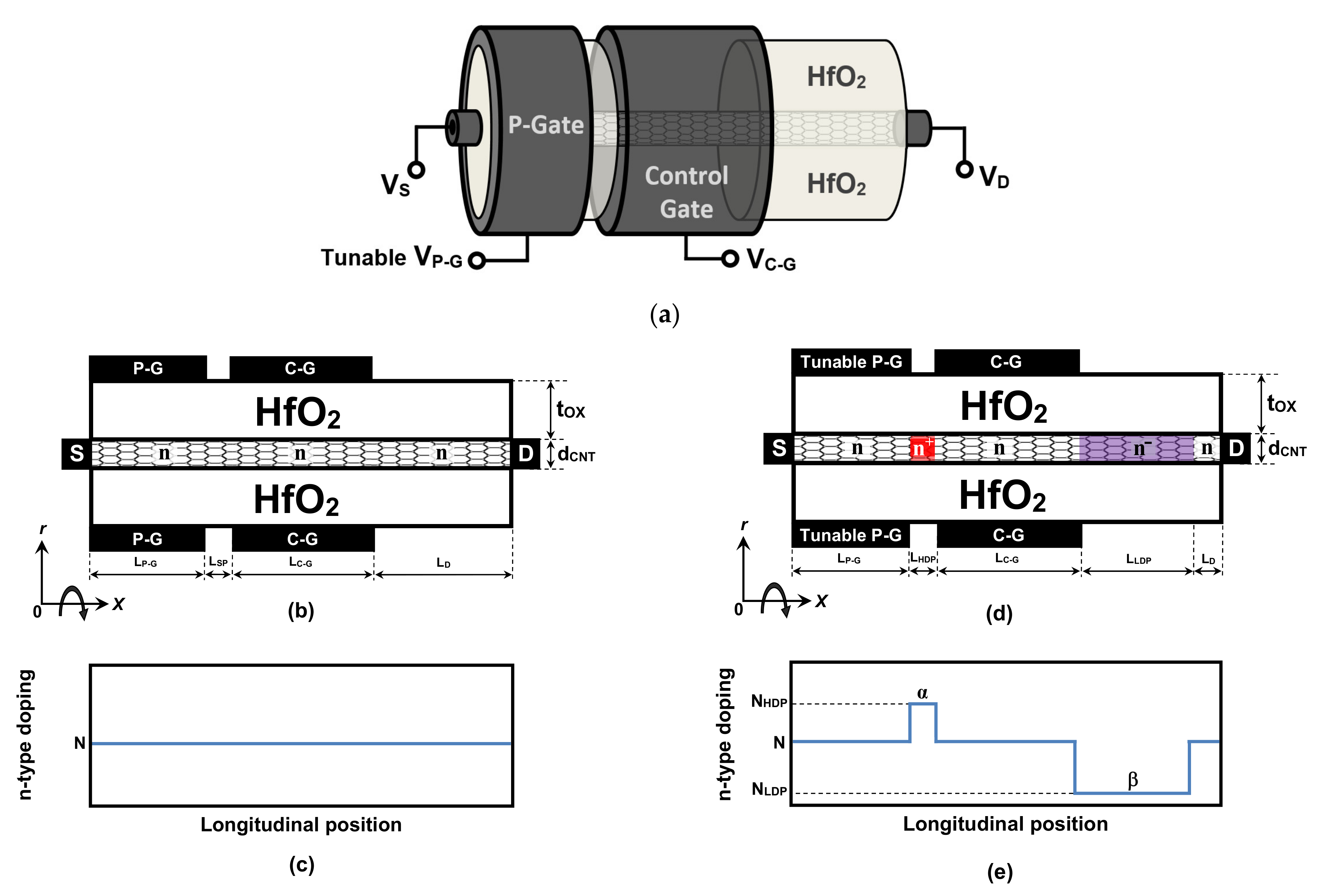
2. Device Structure
3. Simulation Approach
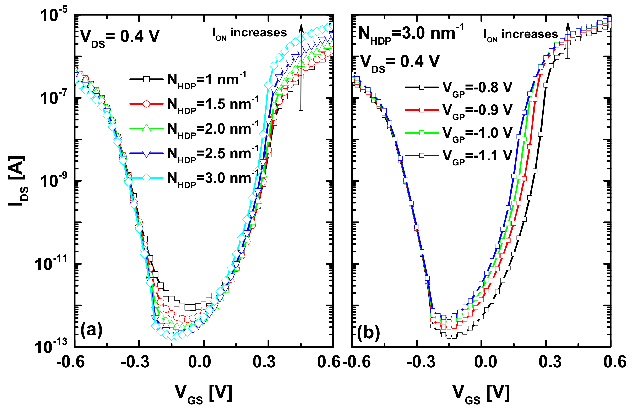
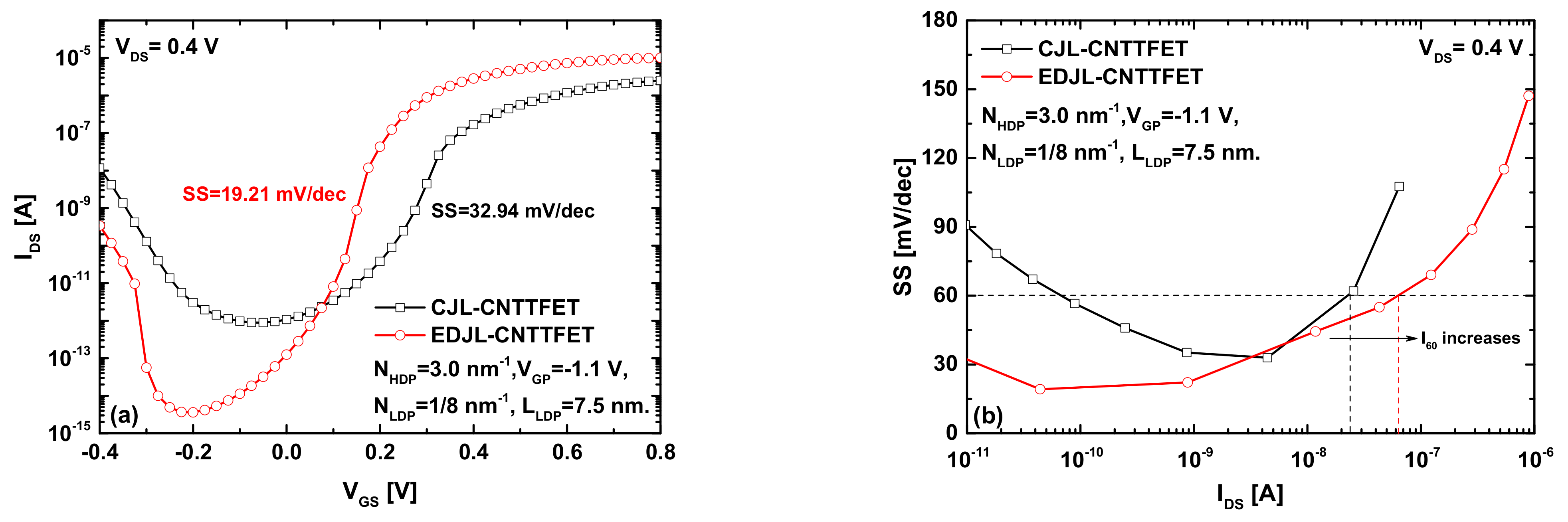
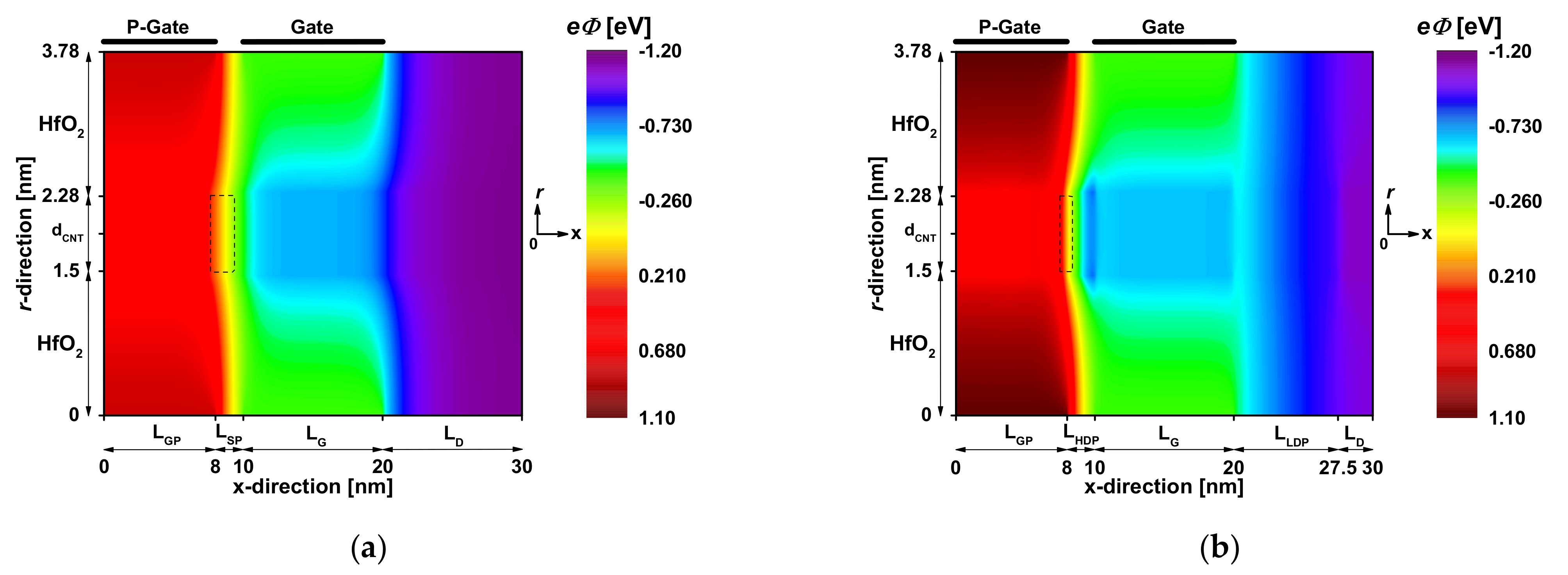
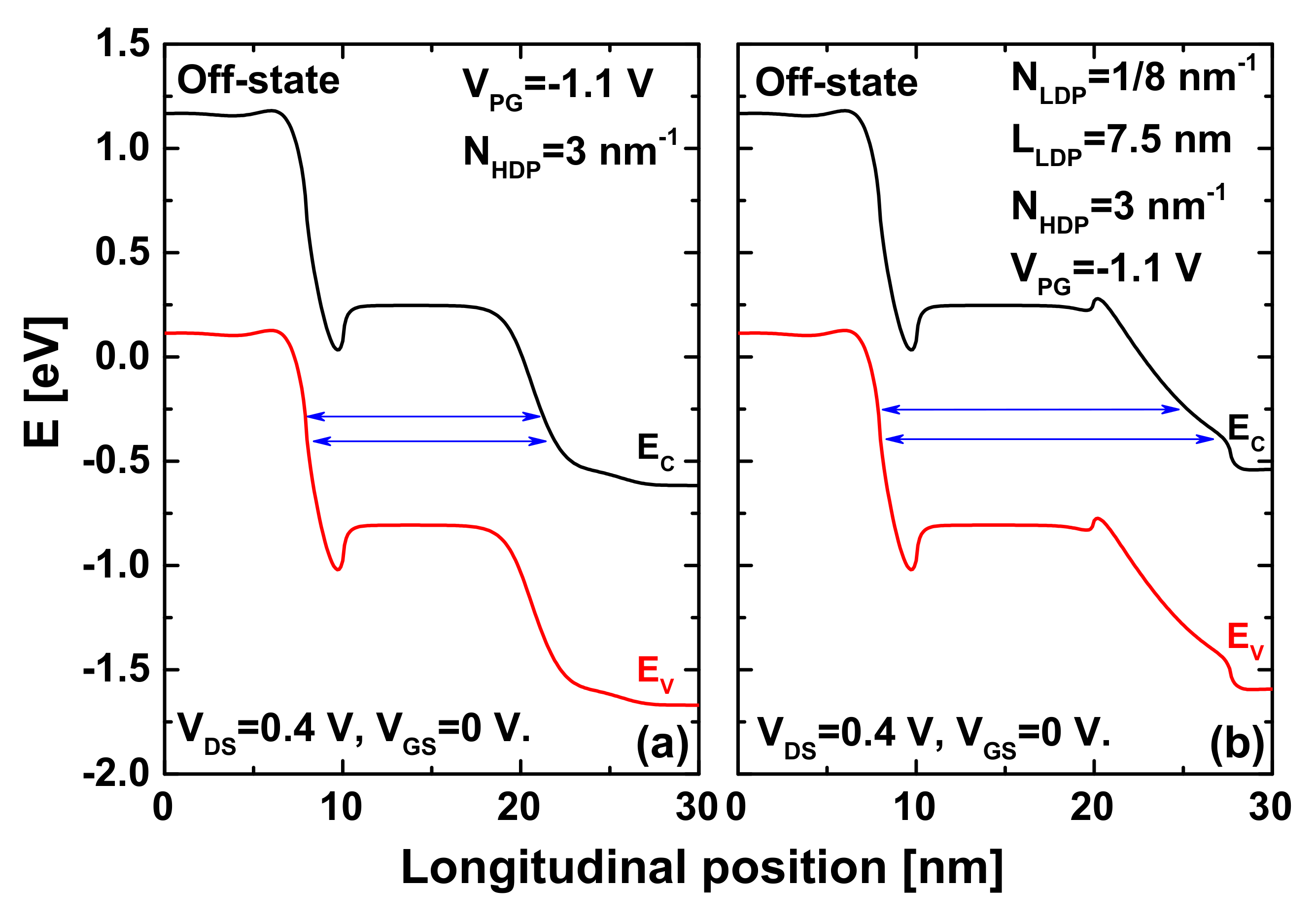
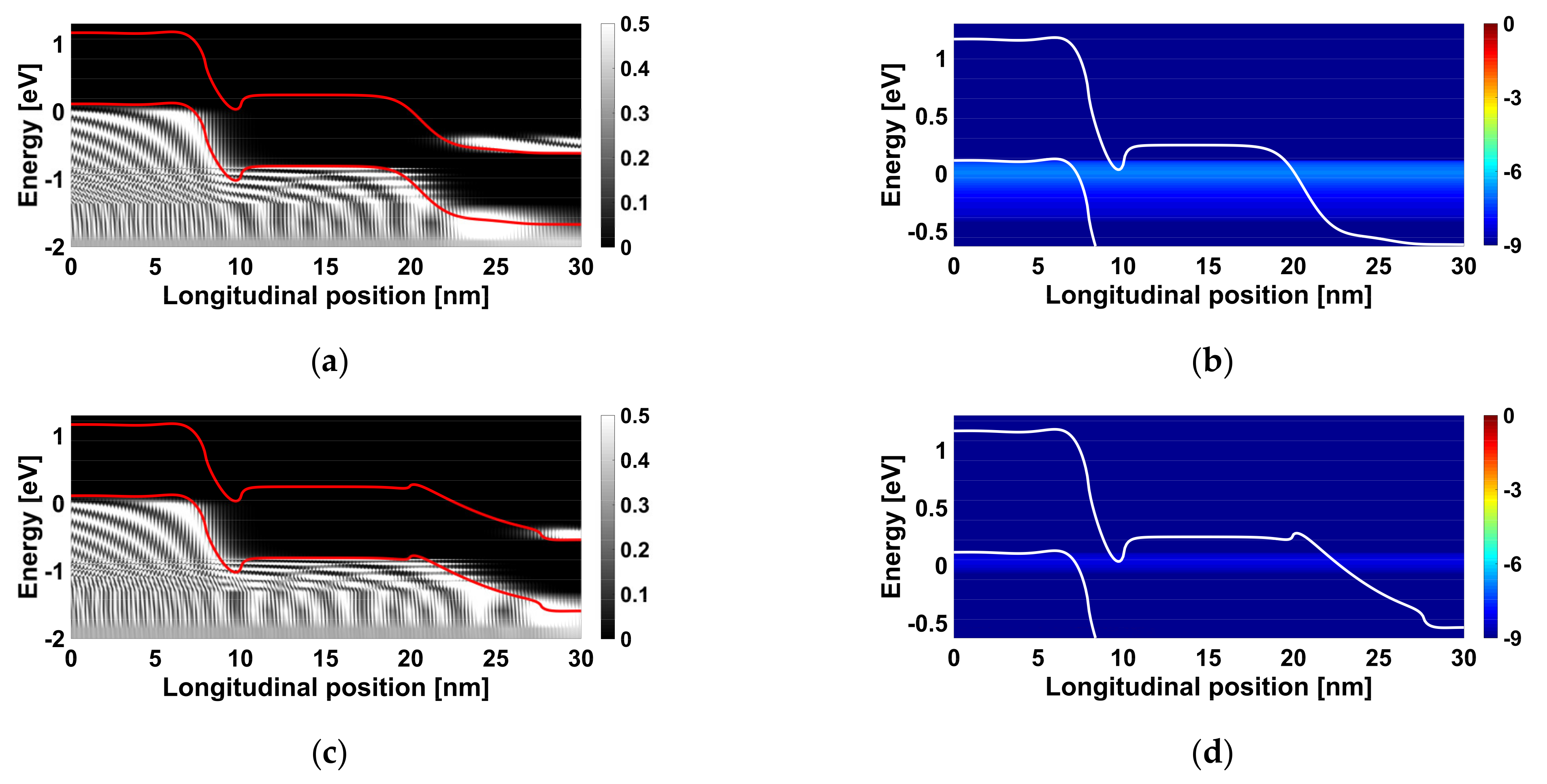
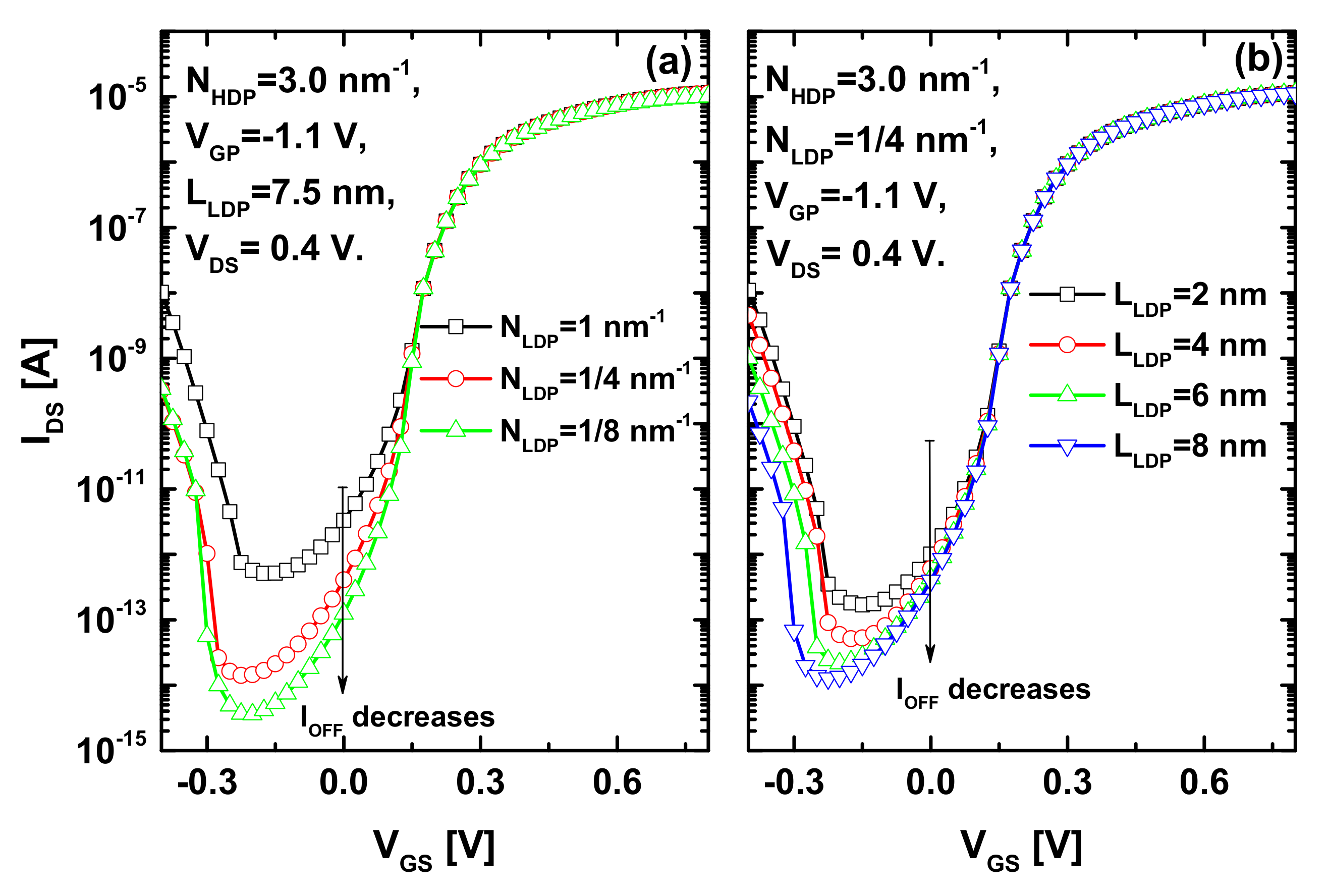
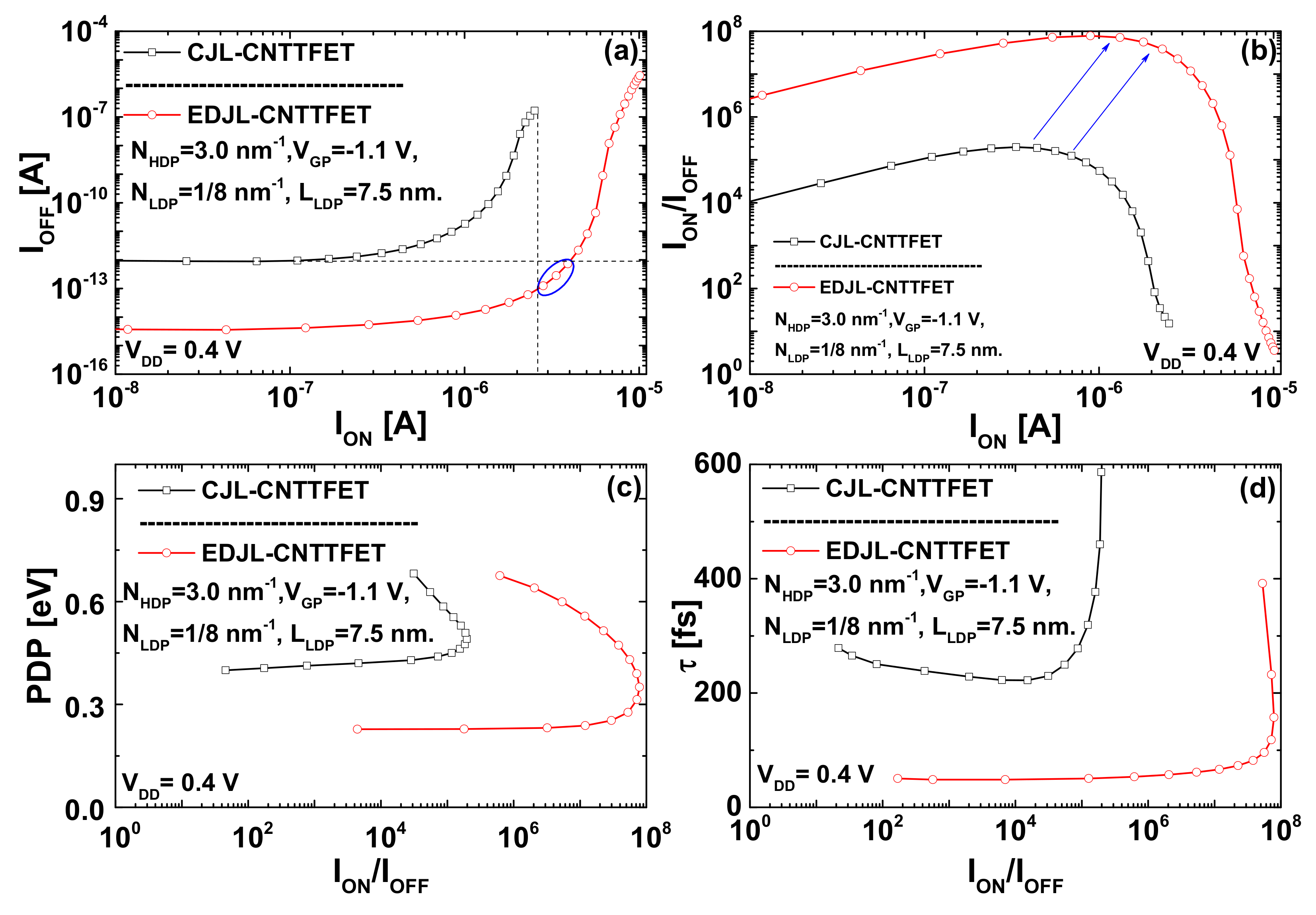
4. Results and Discussion
5. Conclusions
Author Contributions
Funding
Institutional Review Board Statement
Informed Consent Statement
Data Availability Statement
Acknowledgments
Conflicts of Interest
References
- Ionescu, A.M.; Riel, H. Tunnel field-effect transistors as energy-efficient electronic switches. Nature 2011, 479, 329–337. [Google Scholar] [CrossRef] [PubMed]
- Sarkar, D.; Xie, X.; Liu, W.; Cao, W.; Kang, J.; Gong, Y.; Kraemer, S.; Ajayan, P.M.; Banerjee, K. A subthermionic tunnel field-effect transistor with an atomically thin channel. Nature 2015, 526, 91–95. [Google Scholar] [CrossRef] [PubMed]
- Avci, U.E.; Morris, D.H.; Young, I. Tunnel Field-Effect Transistors: Prospects and Challenges. IEEE J. Electron Devices Soc. 2015, 3, 88–95. [Google Scholar] [CrossRef]
- Lu, H.; Lu, B.; Zhang, Y.; Zhang, Y.; Lv, Z. Drain Current Model for Double Gate Tunnel-FETs with InAs/Si Heterojunction and Source-Pocket Architecture. Nanomaterials 2019, 9, 181. [Google Scholar] [CrossRef] [Green Version]
- Tamersit, K. A novel band-to-band tunneling junctionless carbon nanotube field-effect transistor with lightly doped pocket: Proposal, assessment, and quantum transport analysis. Phys. E Low-Dimens. Syst. Nanostruct. 2021, 128, 114609. [Google Scholar] [CrossRef]
- Tamersit, K. New nanoscale band-to-band tunneling junctionless GNRFETs: Potential high-performance devices for the ultrascaled regime. J. Comput. Electron. 2021, 20, 1147–1156. [Google Scholar] [CrossRef]
- Lee, C.-W.; Afzalian, A.; Akhavan, N.D.; Yan, R.; Ferain, I.; Colinge, J.-P. Junctionless multigate field-effect transistor. Appl. Phys. Lett. 2009, 94, 053511. [Google Scholar] [CrossRef]
- Tamersit, K. Sub-10 nm junctionless carbon nanotube field-effect transistors with improved performance. AEU-Int. J. Electron. Commun. 2020, 124, 153354. [Google Scholar] [CrossRef]
- Ghosh, B.; Akram, M.W. Junctionless Tunnel Field Effect Transistor. IEEE Electron Device Lett. 2013, 34, 584–586. [Google Scholar] [CrossRef]
- Tamersit, K. Improved performance of nanoscale junctionless carbon nanotube tunneling FETs using dual-material source gate design: A quantum simulation study. AEU-Int. J. Electron. Commun. 2020, 127, 153491. [Google Scholar] [CrossRef]
- Tamersit, K. Boosting the performance of an ultrascaled carbon nanotube junctionless tunnel field-effect transistor using an ungated region: NEGF simulation. J. Comput. Electron. 2019, 18, 1222–1228. [Google Scholar] [CrossRef]
- Nguyen, H.P.T.; Murugathas, T.; Plank, N.O. Comparison of Duplex and Quadruplex Folding Structure AdenosineAptamers for Carbon Nanotube Field Effect Transistor Aptasensors. Nanomaterials 2021, 11, 2280. [Google Scholar] [CrossRef] [PubMed]
- Avouris, P.; Chen, Z.; Perebeinos, V. Carbon-based electronics. Nat. Nanotechnol. 2007, 2, 605–615. [Google Scholar] [CrossRef] [PubMed]
- Browning, L.; Watterson, W.; Happe, E.; Silva, S.; Valenzuela, R.A.; Smith, J.; Dierkes, M.; Taylor, R.; Plank, N.; Marlow, C. Investigation of Fractal Carbon Nanotube Networks for Biophilic Neural Sensing Applications. Nanomaterials 2021, 11, 636. [Google Scholar] [CrossRef]
- La Mura, M.; Lamberti, P.; Tucci, V. Numerical Evaluation of the Effect of Geometric Tolerances on the High-Frequency Performance of Graphene Field-Effect Transistors. Nanomaterials 2021, 11, 3121. [Google Scholar] [CrossRef]
- Shirazi, S.G.; Karimi, G.R.; Mirzakuchaki, S. GAA CNT TFETs structural engineering: A higher on current, lower ambipolarity. IEEE Trans. Electron Devices 2019, 66, 2822–2830. [Google Scholar] [CrossRef]
- Poli, S.; Reggiani, S.; Gnudi, A.; Gnani, E.; Baccarani, G. Computational Study of the Ultimate Scaling Limits of CNT Tunneling Devices. IEEE Trans. Electron Devices 2007, 55, 313–321. [Google Scholar] [CrossRef]
- Tamersit, K. Computational Study of p-n Carbon Nanotube Tunnel Field-Effect Transistor. IEEE Trans. Electron Devices 2020, 67, 704–710. [Google Scholar] [CrossRef]
- Tamersit, K. Improved Switching Performance of Nanoscale p-i-n Carbon Nanotube Tunneling Field-Effect Transistors Using Metal-Ferroelectric-Metal Gating Approach. ECS J. Solid State Sci. Technol. 2021, 10, 031004. [Google Scholar] [CrossRef]
- Yoon, Y.; Salahuddin, S. Barrier-free tunneling in a carbon heterojunction transistor. Appl. Phys. Lett. 2010, 97, 33102. [Google Scholar] [CrossRef] [Green Version]
- Gu, J.; Zhang, Q.; Wu, Z.; Yao, J.; Zhang, Z.; Zhu, X.; Wang, G.; Li, J.; Zhang, Y.; Cai, Y.; et al. Cryogenic Transport Characteristics of P-Type Gate-All-Around Silicon Nanowire MOSFETs. Nanomaterials 2021, 11, 309. [Google Scholar] [CrossRef] [PubMed]
- Guo, J.; Datta, S.; Lundstrom, M.; Anantam, M.P. Toward Multiscale Modeling of Carbon Nanotube Transistors. Int. J. Multiscale Comput. Eng. 2004, 2, 257–276. [Google Scholar] [CrossRef]
- Tamersit, K. Improving the On-Current of Junctionless Carbon Nanotube Tunneling FETs Using a Heavily n-Type Doped Pocket. In Proceedings of the 2021 International Semiconductor Conference (CAS), Sinaia, Romania, 6–8 October 2021; pp. 257–260. [Google Scholar] [CrossRef]
- Tamersit, K. Performance Assessment of a New Radiation Dosimeter Based on Carbon Nanotube Field-Effect Transistor: A Quantum Simulation Study. IEEE Sens. J. 2019, 19, 3314–3321. [Google Scholar] [CrossRef]
- Tamersit, K.; Jooq, M.K.Q.; Moaiyeri, M.H. Analog/RF performance assessment of ferroelectric junctionless carbon nanotube FETs: A quantum simulation study. Phys. E Low-Dimens. Syst. Nanostruct. 2021, 134, 114915. [Google Scholar] [CrossRef]
- Datta, S. Nanoscale device modeling: The Green’s function method. Superlattices Microstruct. 2000, 28, 253–278. [Google Scholar] [CrossRef]
- Koswatta, S.O.; Hasan, S.; Lundstrom, M.S.; Anantram, M.P.; Nikonov, D. Nonequilibrium Green’s Function Treatment of Phonon Scattering in Carbon-Nanotube Transistors. IEEE Trans. Electron Devices 2007, 54, 2339–2351. [Google Scholar] [CrossRef] [Green Version]
- Tamersit, K. Quantum simulation of a junctionless carbon nanotube field-effect transistor with binary metal alloy gate electrode. Superlattices Microstruct. 2019, 128, 252–259. [Google Scholar] [CrossRef]
- Tamersit, K. Improving the performance of a junctionless carbon nanotube field-effect transistor using a split-gate. AEU-Int. J. Electron. Commun. 2020, 115, 153035. [Google Scholar] [CrossRef]
- Lu, H.; Seabaugh, A. Tunnel Field-Effect Transistors: State-of-the-Art. IEEE J. Electron Devices Soc. 2014, 2, 44–49. [Google Scholar] [CrossRef]
- Javey, A.; Tu, R.; Farmer, D.B.; Guo, J.; Gordon, R.G.; Dai, H. High Performance n-Type Carbon Nanotube Field-Effect Transistors with Chemically Doped Contacts. Nano Lett. 2005, 5, 345–348. [Google Scholar] [CrossRef] [Green Version]
- Tamersit, K. Performance enhancement of an ultra-scaled double-gate graphene nanoribbon tunnel field-effect transistor using channel doping engineering: Quantum simulation study. AEU-Int. J. Electron. Commun. 2020, 122, 153287. [Google Scholar] [CrossRef]
- Tamersit, K. A new ultra-scaled graphene nanoribbon junctionless tunneling field-effect transistor: Proposal, quantum simulation, and analysis. J. Comput. Electron. 2019, 19, 170–176. [Google Scholar] [CrossRef]
- Salahuddin, S.; Datta, S. Use of Negative Capacitance to Provide Voltage Amplification for Low Power Nanoscale Devices. Nano Lett. 2007, 8, 405–410. [Google Scholar] [CrossRef]
- Wong, J.C.; Salahuddin, S. Negative Capacitance Transistors. Proc. IEEE 2019, 107, 49–62. [Google Scholar] [CrossRef]
- Tu, L.; Wang, X.; Wang, J.; Meng, X.; Chu, J. Ferroelectric Negative Capacitance Field Effect Transistor. Adv. Electron. Mater. 2018, 4, 1800231. [Google Scholar] [CrossRef]
- Srimani, T.; Hills, G.; Bishop, M.D.; Radhakrishna, U.; Zubair, A.; Park, R.S.; Stein, Y.; Palacios, T.; Antoniadis, D.; Shulaker, M.M. Negative Capacitance Carbon Nanotube FETs. IEEE Electron Device Lett. 2017, 39, 304–307. [Google Scholar] [CrossRef]
- Saeidi, A.; Jazaeri, F.; Stolichnov, I.; Luong, G.V.; Zhao, Q.-T.; Mantl, S.; Ionescu, A.M. Effect of hysteretic and non-hysteretic negative capacitance on tunnel FETs DC performance. Nanotechnology 2018, 29, 095202. [Google Scholar] [CrossRef] [Green Version]
- Sakib, F.I.; Mullick, F.E.; Shahnewaz, S.; Islam, S.; Hossain, M. Influence of device architecture on the performance of negative capacitance MFMIS transistors. Semicond. Sci. Technol. 2019, 35, 025005. [Google Scholar] [CrossRef]
- Jiang, C.; Liang, R.; Xu, J. Investigation of Negative Capacitance Gate-all-around Tunnel FETs Combining Numerical Simulation and Analytical Modeling. IEEE Trans. Nanotechnol. 2016, 16, 58–67. [Google Scholar] [CrossRef]
- Seo, J.; Lee, J.; Shin, M. Analysis of Drain-Induced Barrier Rising in Short-Channel Negative-Capacitance FETs and Its Applications. IEEE Trans. Electron Devices 2017, 64, 1793–1798. [Google Scholar] [CrossRef]
- Sakib, F.I.; Hasan, A.; Hossain, M. Exploration of Negative Capacitance in Gate-All-Around Si Nanosheet Transistors. IEEE Trans. Electron Devices 2020, 67, 5236–5242. [Google Scholar] [CrossRef]
- Behbahani, F.; Jooq, M.K.Q.; Moaiyeri, M.H.; Tamersit, K. Leveraging Negative Capacitance CNTFETs for Image Processing: An Ultra-Efficient Ternary Image Edge Detection Hardware. IEEE Trans. Circuits Syst. I Regul. Pap. 2021, 68, 5108–5119. [Google Scholar] [CrossRef]
- Jooq, M.K.Q.; Moaiyeri, M.H.; Tamersit, K. Ultra-Compact Ternary Logic Gates Based on Negative Capacitance Carbon Nanotube FETs. IEEE Trans. Circuits Syst. II Express Briefs 2020, 68, 2162–2166. [Google Scholar] [CrossRef]
- Tamersit, K.; Jooq, M.K.Q.; Moaiyeri, M.H. Computational Investigation of Negative Capacitance Coaxially Gated Carbon Nanotube Field-Effect Transistors. IEEE Trans. Electron Devices 2020, 68, 376–384. [Google Scholar] [CrossRef]
- Dabhi, C.K.; Parihar, S.S.; Dasgupta, A.; Chauhan, Y.S. Compact Modeling of Negative-Capacitance FDSOI FETs for Circuit Simulations. IEEE Trans. Electron Devices 2020, 67, 2710–2716. [Google Scholar] [CrossRef]
- Dutta, T.; Pahwa, G.; Agarwal, A.; Chauhan, Y.S. Impact of Process Variations on Negative Capacitance FinFET Devices and Circuits. IEEE Electron Device Lett. 2017, 39, 147–150. [Google Scholar] [CrossRef]
- Tamersit, K.; Kotti, M.; Fakhfakh, M. A new pressure microsensor based on dual-gate graphene field-effect transistor with a vertically movable top-gate: Proposal, analysis, and optimization. AEU-Int. J. Electron. Commun. 2020, 124, 153346. [Google Scholar] [CrossRef]
- Bae, G.Y.; Kim, J.; Kim, J.; Lee, S.; Lee, E. MoTe2 Field-Effect Transistors with Low Contact Resistance through Phase Tuning by Laser Irradiation. Nanomaterials 2021, 11, 2805. [Google Scholar] [CrossRef]
- Tamersit, K.; Ramezani, Z.; Amiri, I. Improved performance of sub-10-nm band-to-band tunneling n-i-n graphene nanoribbon field-effect transistors using underlap engineering: A quantum simulation study. J. Phys. Chem. Solids 2021, 160, 110312. [Google Scholar] [CrossRef]
- Zhang, Q.; Iannaccone, G.; Fiori, G. Two-dimensional tunnel transistors based on Bi2Se3 thin film. IEEE Electron Device Lett. 2014, 35, 129–131. [Google Scholar] [CrossRef]
- Chen, C.-Y.; Ameen, T.A.; Ilatikhameneh, H.; Rahman, R.; Klimeck, G.; Appenzeller, J. Channel Thickness Optimization for Ultrathin and 2-D Chemically Doped TFETs. IEEE Trans. Electron Devices 2018, 65, 4614–4621. [Google Scholar] [CrossRef]
- Liu, F.; Zhou, Y.; Wang, Y.; Liu, X.; Wang, J.; Guo, H. Negative capacitance transistors with monolayer black phosphorus. Npj Quantum Mater. 2016, 1, 16004. [Google Scholar] [CrossRef]
- Ilatikhameneh, H.; Tan, Y.; Novakovic, B.; Klimeck, G.; Rahman, R.; Appenzeller, J. Tunnel Field-Effect Transistors in 2-D Transition Metal Dichalcogenide Materials. IEEE J. Explor. Solid-State Comput. Devices Circuits 2015, 1, 12–18. [Google Scholar] [CrossRef]
- Fiori, G.; Bonaccorso, F.; Iannaccone, G.; Palacios, T.; Neumaier, D.; Seabaugh, A.; Banerjee, S.K.; Colombo, L. Electronics based on two-dimensional materials. Nat. Nanotechnol. 2014, 9, 768–779. [Google Scholar] [CrossRef] [PubMed]
- Ilatikhameneh, H.; Klimeck, G.; Rahman, R. Can Homojunction Tunnel FETs Scale Below 10 nm? IEEE Electron Device Lett. 2015, 37, 115–118. [Google Scholar] [CrossRef] [Green Version]
- Marin, E.G.; Marian, D.; Iannaccone, G.; Fiori, G. First principles investigation of tunnel FETs based on nanoribbons from topological two-dimensional materials. Nanoscale 2017, 9, 19390–19397. [Google Scholar] [CrossRef] [Green Version]
- Tamersit, K.; Djeffal, F. Double-Gate Graphene Nanoribbon Field-Effect Transistor for DNA and Gas Sensing Applications: Simulation Study and Sensitivity Analysis. IEEE Sens. J. 2016, 16, 4180–4191. [Google Scholar] [CrossRef]
- Tamersit, K.; Djeffal, F. Carbon Nanotube Field-Effect Transistor with Vacuum Gate Dielectric for Label-Free Detection of DNA Molecules: A Computational Investigation. IEEE Sens. J. 2019, 19, 9263–9270. [Google Scholar] [CrossRef]
- Anvarifard, M.K.; Ramezani, Z.; Amiri, I.S.; Tamersit, K.; Nejad, A.M. Profound analysis on sensing performance of Nanogap SiGe source DM-TFET biosensor. J. Mater. Sci. Mater. Electron. 2020, 31, 22699–22712. [Google Scholar] [CrossRef]
- Tamersit, K. An ultra-sensitive gas nanosensor based on asymmetric dual-gate graphene nanoribbon field-effect transistor: Proposal and investigation. J. Comput. Electron. 2019, 18, 846–855. [Google Scholar] [CrossRef]


| Parameter | Symbol | Value | Unit |
|---|---|---|---|
| Common parameters | |||
| Z-CNT | (n,0) | 10 | - |
| Gap energy | EG | ~1.053 | eV |
| CNT diameter | dCNT | ~7.82 | Å |
| Gate length | LC-G | 10 | nm |
| Drain length | LD | 10 | nm |
| P-gate length | LP-G | 8 | nm |
| Space between gates | LSP | 2 | nm |
| S/C/D doping (CJL) | N | 1 | nm−1 |
| Oxide thickness | tOX | 1.5 | nm |
| HfO2 dielectric constant | εOX | 16 | - |
| Temperature | T | 300 | K |
| Source gate voltage | VP-G | −0.8 | V |
| Drain-to-source voltage | VDS | 0.4 | V |
| Additional parameters in the proposed design | |||
| Heavily doped pocket | NHDP | 3 | nm−1 |
| HDP Length | LHDP | 2 | nm |
| Lightly doped pocket | NLDP | N/8 | nm−1 |
| LDP Length | LLDP | 7.5 | nm |
| Parameter | CJL-CNTTFET | EDJL-CNTTFET |
|---|---|---|
| ION (A) | 7 × 10⁻⁷ | 1.34 × 10⁻⁶ |
| IOFF (A) | 3.4 × 10⁻⁹ | 1.23 × 10⁻¹¹ |
| IMIN (μA) | 1.41 × 10⁻³ | 2.05 × 10⁻⁶ |
| I60 (A) | - | 5.6 × 10⁻⁸ |
| ION/IOFF | 205.8 | 105 |
| SS (mV/dec) | 128 | 43 |
| PDP (eV) | 0.52 | 0.31 |
| τ (fs) | 300.8 | 94.3 |
Publisher’s Note: MDPI stays neutral with regard to jurisdictional claims in published maps and institutional affiliations. |
© 2022 by the authors. Licensee MDPI, Basel, Switzerland. This article is an open access article distributed under the terms and conditions of the Creative Commons Attribution (CC BY) license (https://creativecommons.org/licenses/by/4.0/).
Share and Cite
Tamersit, K.; Kouzou, A.; Bourouba, H.; Kennel, R.; Abdelrahem, M. Synergy of Electrostatic and Chemical Doping to Improve the Performance of Junctionless Carbon Nanotube Tunneling Field-Effect Transistors: Ultrascaling, Energy-Efficiency, and High Switching Performance. Nanomaterials 2022, 12, 462. https://doi.org/10.3390/nano12030462
Tamersit K, Kouzou A, Bourouba H, Kennel R, Abdelrahem M. Synergy of Electrostatic and Chemical Doping to Improve the Performance of Junctionless Carbon Nanotube Tunneling Field-Effect Transistors: Ultrascaling, Energy-Efficiency, and High Switching Performance. Nanomaterials. 2022; 12(3):462. https://doi.org/10.3390/nano12030462
Chicago/Turabian StyleTamersit, Khalil, Abdellah Kouzou, Hocine Bourouba, Ralph Kennel, and Mohamed Abdelrahem. 2022. "Synergy of Electrostatic and Chemical Doping to Improve the Performance of Junctionless Carbon Nanotube Tunneling Field-Effect Transistors: Ultrascaling, Energy-Efficiency, and High Switching Performance" Nanomaterials 12, no. 3: 462. https://doi.org/10.3390/nano12030462
APA StyleTamersit, K., Kouzou, A., Bourouba, H., Kennel, R., & Abdelrahem, M. (2022). Synergy of Electrostatic and Chemical Doping to Improve the Performance of Junctionless Carbon Nanotube Tunneling Field-Effect Transistors: Ultrascaling, Energy-Efficiency, and High Switching Performance. Nanomaterials, 12(3), 462. https://doi.org/10.3390/nano12030462