Article

Resistive Switching Memory Cell Property Improvement by Al/SrZrTiO3/Al/SrZrTiO3/ITO with Embedded Al Layer

1
Institute of Microelectronics, Department of Electrical Engineering, National Cheng-Kung University, Tainan 701, Taiwan
2
Program on Semiconductor Process Technology, Academy of Innovative Semiconductor and Sustainable Manufacturing, National Cheng-Kung University, Tainan 701, Taiwan
3
Department of Physics, National Sun Yat-sen University, Kaohsiung 804, Taiwan
*
Author to whom correspondence should be addressed.
Nanomaterials 2022, 12(24), 4412; https://doi.org/10.3390/nano12244412
Submission received: 11 November 2022 / Revised: 5 December 2022 / Accepted: 8 December 2022 / Published: 10 December 2022
(This article belongs to the Special Issue Memory Nanomaterials: Growth, Characterization and Device Fabrication)

Abstract

:
The SrZrTiO3 (SZT) thin film prepared by sol-gel process for the insulator of resistive random-access memory (RRAM) is presented. Al was embedded in the SZT thin film to enhance the switching characteristics. Compared with the pure SZT thin-film RRAM, the RRAM with the embedded Al in SZT thin film demonstrated outstanding device parameter improvements, such as a resistance ratio higher than 107, lower operation voltage (VSET = −0.8 V and VRESET = 2.05 V), uniform film, and device stability of more than 105 s. The physical properties of the SZT thin film and the embedded-Al SZT thin-film RRAM devices were probed.

1. Introduction

Among various candidates for nonvolatile memories, resistive random-access memory (RRAM) attracts considerable attention owing to its advantages, such as simple metal–insulator–metal (MIM) structure, fast operation speed, low operation voltage, and low fabrication temperature. Numerous materials, such as transition metal oxides (HfO2, TiO2, and NiO), organic material (composites containing nanoparticles and polyimide), or perovskite oxides (SrZrO3 and SrTiO3), have been investigated as potential materials for RRAMs. In this study, we focused on the SrTiO3 material because of its high dielectric constant, low dielectric loss, tenability, high breakdown strength, low leakage current, and great film quality [1]. Numerous attempts have been exerted to further improve the properties of SrTiO3-based ceramics. Doping is considered an effective approach for altering their properties [2]. Reproducible resistive switching behaviors have been observed in doped perovskite oxide films [3,4], such as Mo-doped SrTiO3 [5], Mg-doped SrTiO3 [6], Nb-doped SrTiO3 films [7], and Ni-doped SrTiO3 films [3]. Several studies have indicated that Zr4+ in SrTiO3 can stabilize the charge of Ti4+ and suppress oxygen dissociation [1,2,8]. In addition, our previous study showed that the addition of Zr can effectively improve the surface morphology of insulators [9]. Moreover, the sol-gel process has advantages, such as low fabrication temperature, low cost, and easy adjustment of proportions. This process can be applied in numerous devices [10]. Based on the above advantages and research results, in this work, we utilized Zr in the doping process to fabricate SrZrTiO3 (SZT) using the sol-gel process for RRAM insulators.
Various inserted metal layers in the insulator layer, including Cu, Pt, and Ti, improve the resistive switching properties of RRAMs [11,12,13,14]. However, a relatively limited number of studies have been performed regarding the mechanism of embedded metal-based RRAM devices. In this study, the effects of Al-included SZT on the resistive switching properties of SZT thin film for RRAM applications were also investigated. For comparison, a memory device with a single-SZT active layer was also fabricated and characterized.

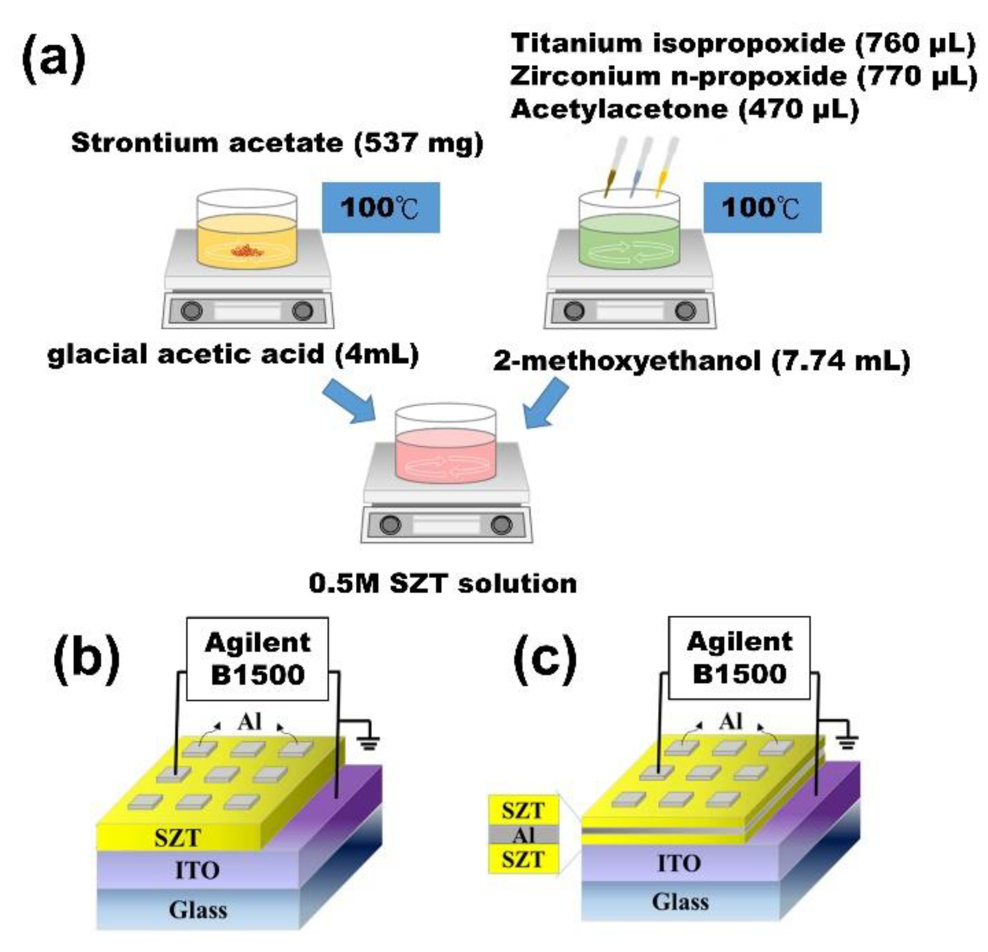
2. Materials and Methods
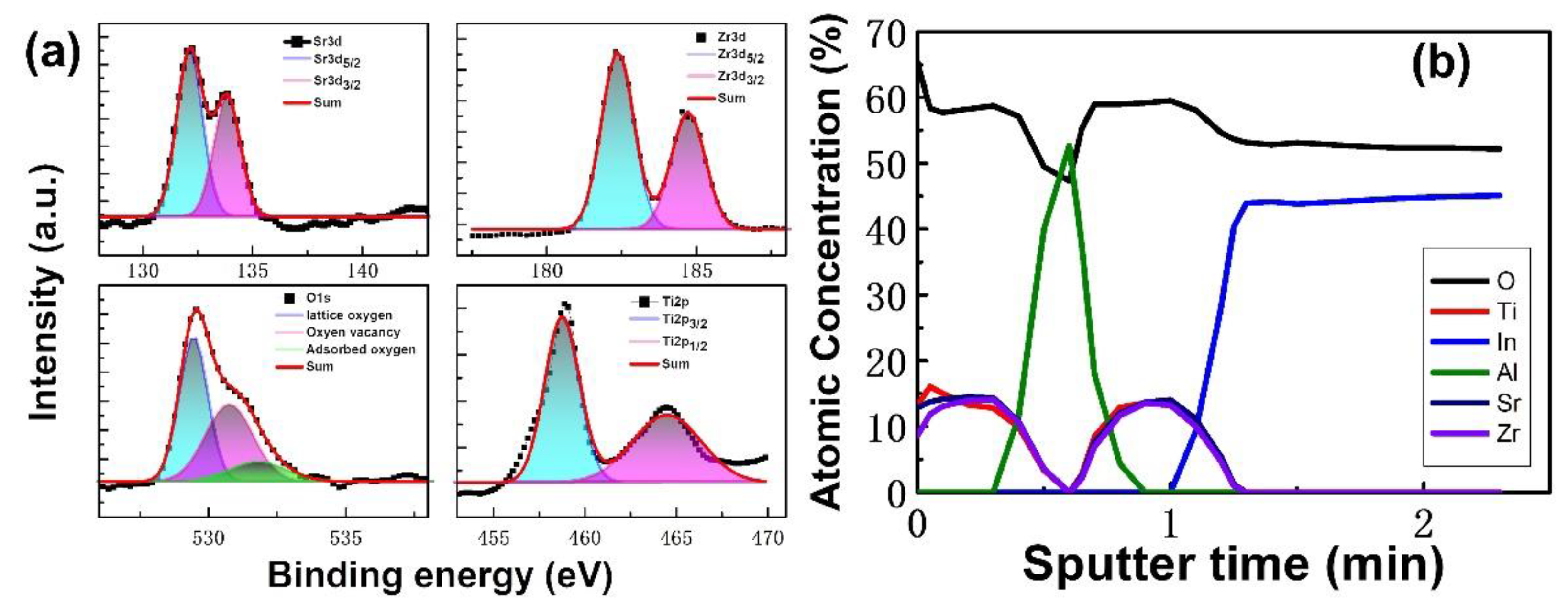
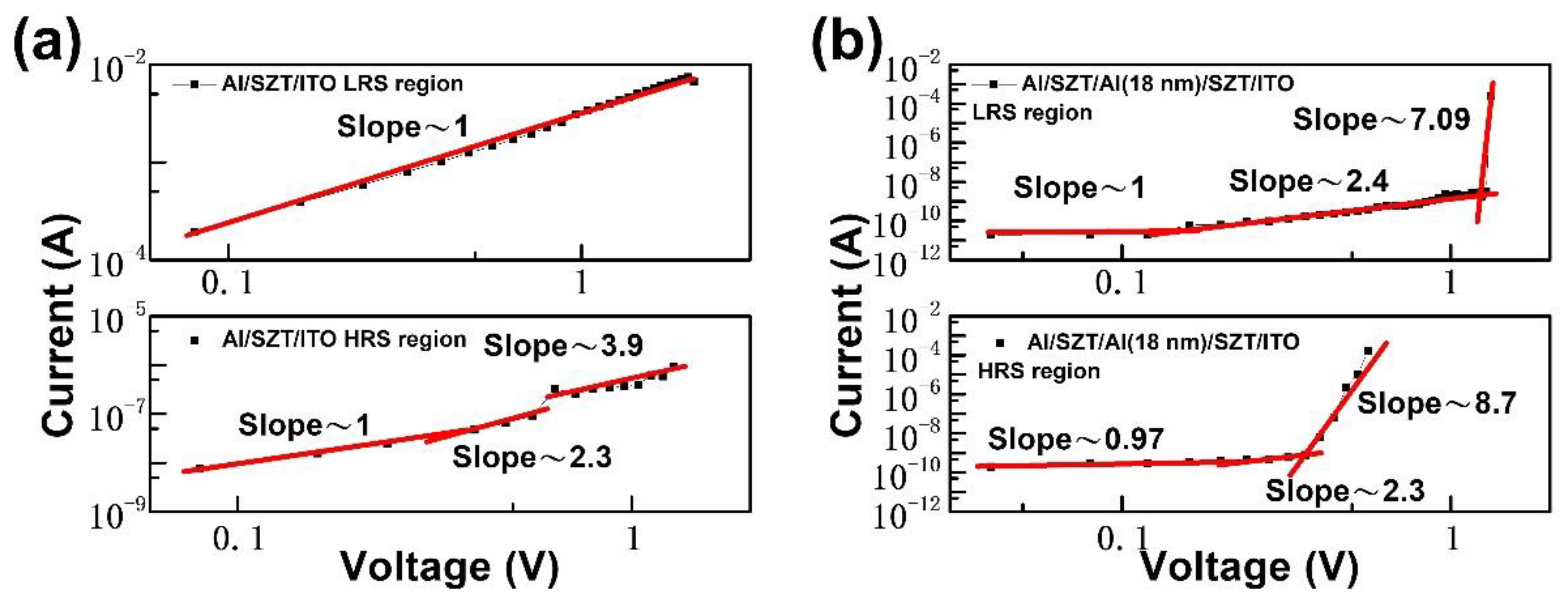
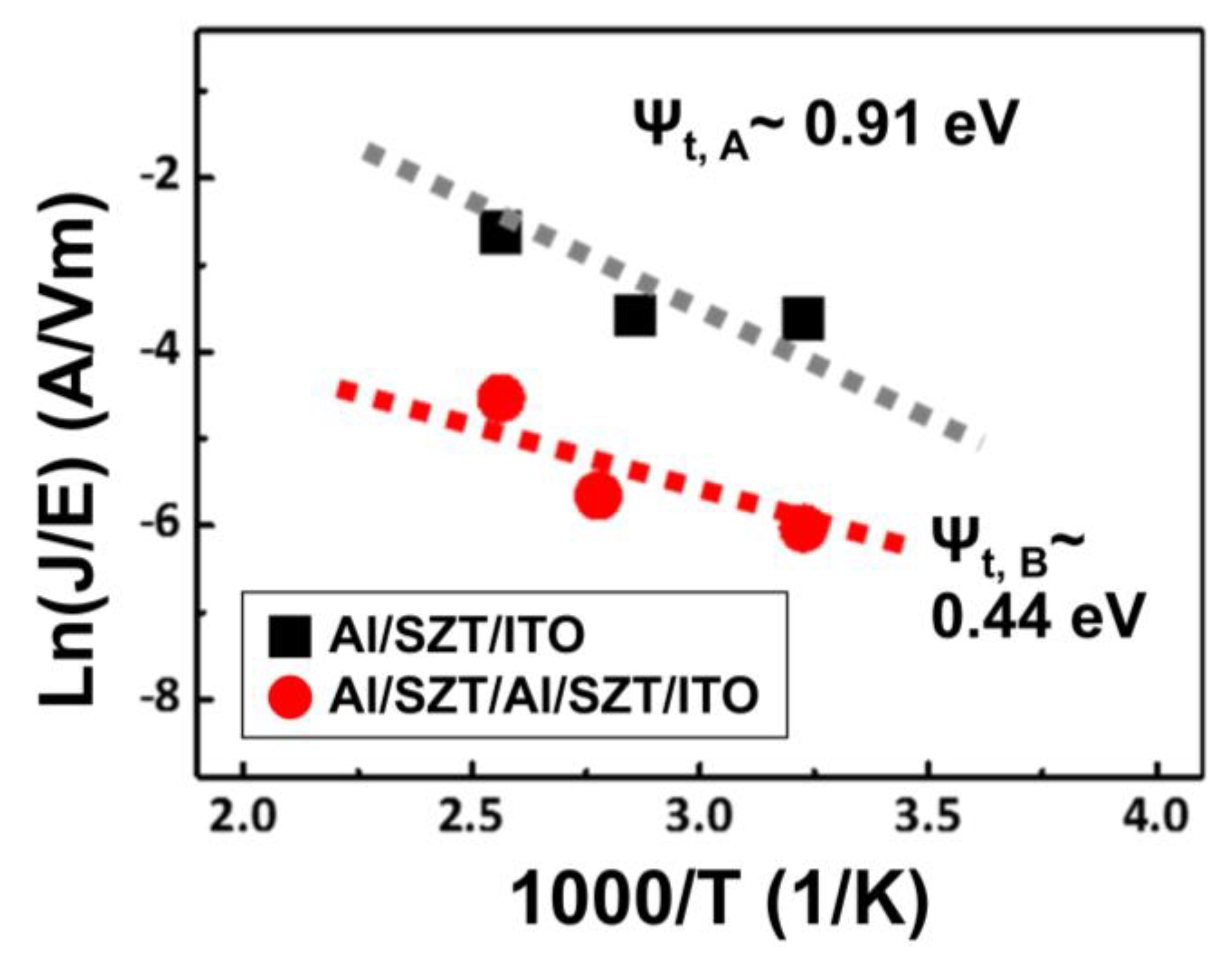
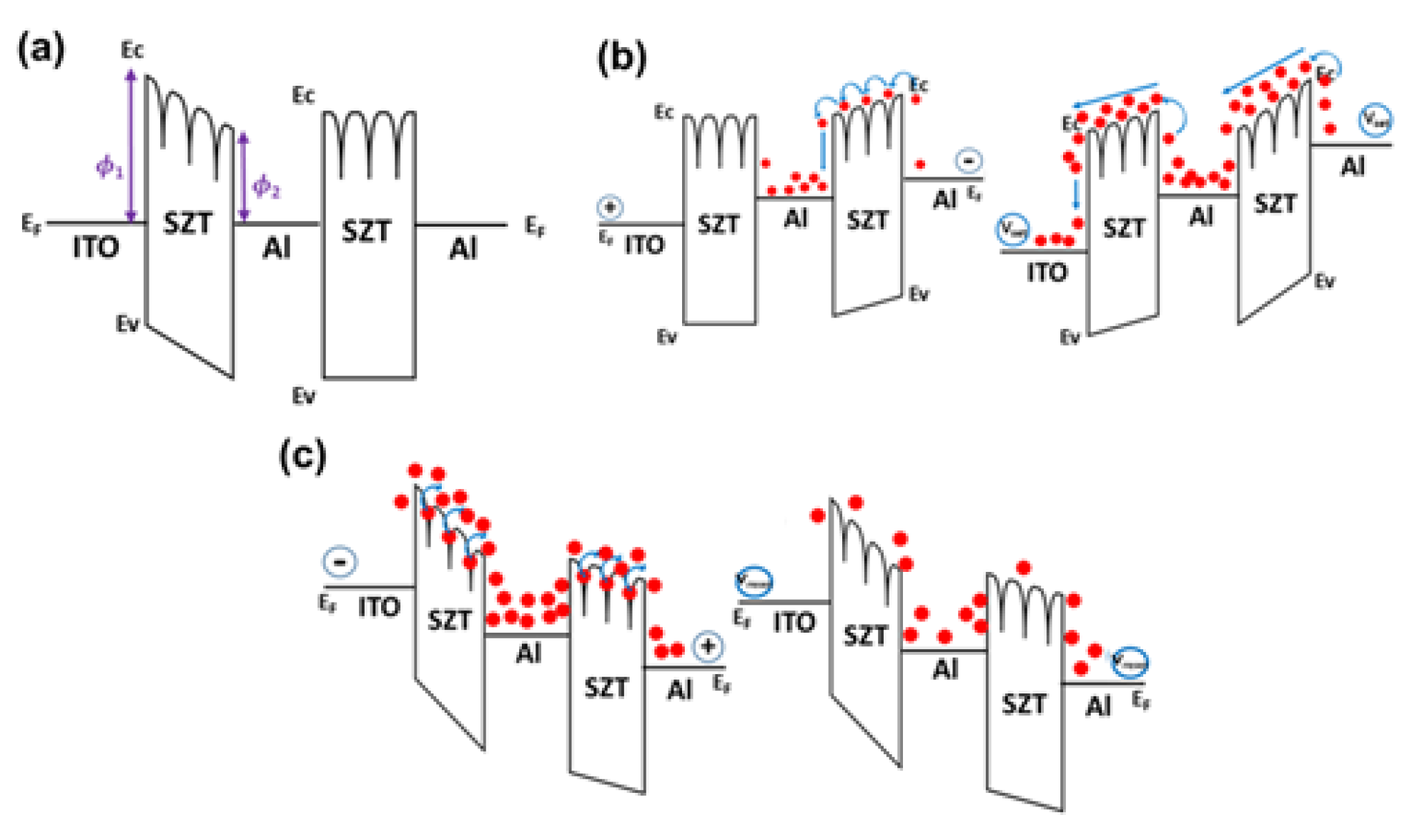
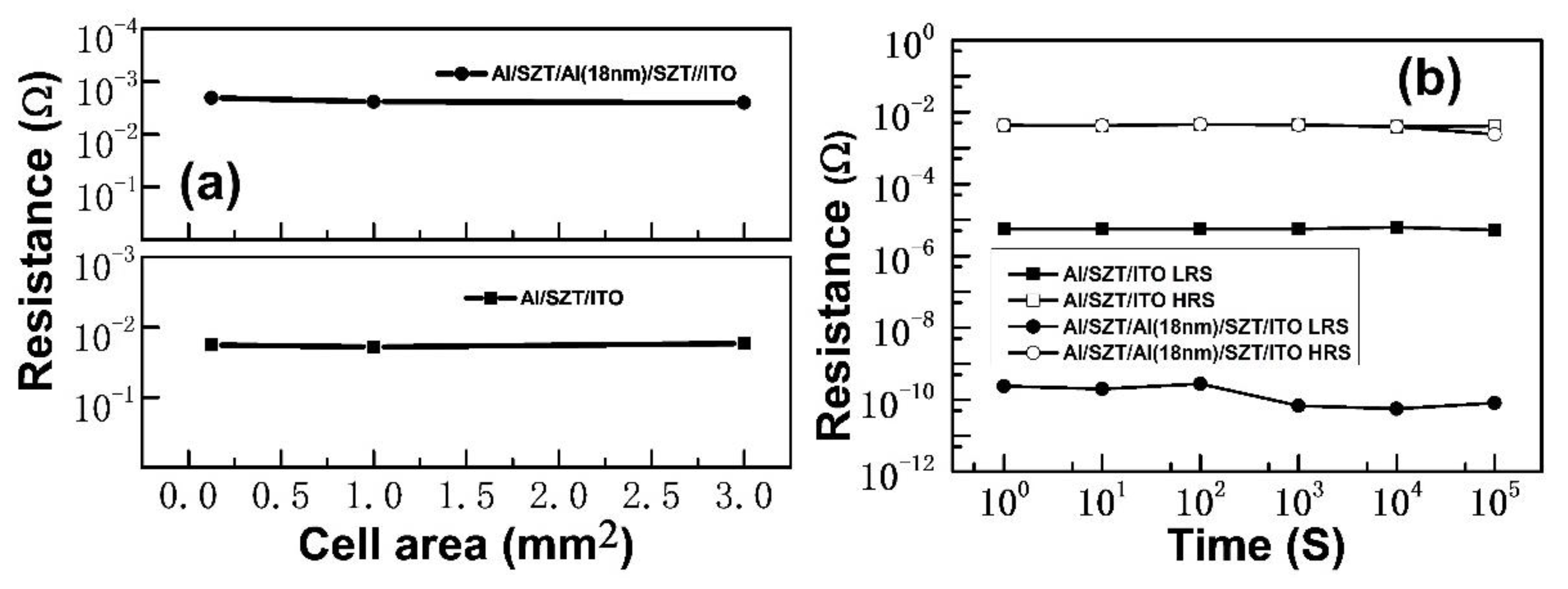
The solutions used in this study were prepared in reference to the previous literature, and the additives and ratios were varied based on experimental requirements [8,15,16]. The 0.5 M SZT solution was prepared in three steps (Figure 1a). First, strontium acetate (537 mg) was dissolved in glacial acetic acid (4 mL) by stirring and then heated on a 100 °C hot plate until complete dissolution (A1 solution). Titanium isopropoxide (760 µL) and zirconium n-propoxide (770 µL) were mixed with acetylacetone (470 µL) and dissolved in 2-methoxyethanol (7.74 mL) by stirring (A2 solution). Finally, A1 was slowly dropped into A2 until a completely transparent solution was obtained (mole proportion of Sr:Zr:Ti was approximately 1:1:1). After chemically cleaning the substrate, the prepared 0.5 M SZT solution was spun coated on an indium tin oxide (ITO)/glass substrate. Each layer was baked at 100 °C for 15 min to remove volatile materials. A 90 nm-thick Al film with an area of 3 mm2 was deposited with a shadow mask using DC magnetron sputtering as the top electrode (TE) of the MIM structure, whereas ITO served as the bottom electrode (BE). Figure 1b shows the schematic configuration of the Al/SZT/ITO structures.
The SZT/Al/SZT tri-layer structure was deposited on the ITO/glass substrate. Both SZT films were prepared through the same process above, and Al was embedded by DC magnetron sputtering. Finally, the same processes were applied for Al TEs. For comparison, we fabricated four different thicknesses of embedded Al layer (5, 18, 25, and 33 nm). Figure 1c displays the schematic configuration of embedded Al in SZT thin-film RRAM devices. Transmission electron microscopy (TEM) analysis was carried out using a JEM-2100F electron microscope. The X-ray diffraction (XRD) spectra were developed via BRUKER, D8 DISCOVER SSS Multi-Function High Power XRD using the copper Kα line with λ = 0.154060 nm. The roughness value and surface morphology of the films were calculated using atomic force microscopy (AFM, Dimension ICON with NanoScope V controller, Bruker, Billerica, MA, USA). X-ray photoelectron spectroscopy (XPS) was performed using a PHI 5000 VersaProbe. Electrical measurements were performed using an Agilent B1500 semiconductor parameter analyzer.

3. Results

Figure 2a presents the TEM image of the cross-sectional SZT/Al/SZT tri-layered thin films sandwiched between ITO BE and Al TE. The estimated thicknesses of the top SZT layer, Al interlayer, and bottom SZT layer were 54, 18, and 67 nm, respectively. The thin films were uniform, and the interfaces were clear. Figure 2b depicts the XRD analysis of the SZT thin film. As shown in the analysis results, no evident peak was observed in the XRD spectrum. The SZT thin film prepared in this experiment had an amorphous phase. Compared with the polycrystalline phase, the amorphous phase is preferred for dielectric layer materials because the former may lead to a high-grain boundary leakage current and a rough film surface [17]. The AFM images in Figure 2c,d reveal the surface morphology of the SZT and SZT/Al/SZT tri-layered thin films. The root-mean-square roughness (Rrms) values of SZT and the SZT/Al/SZT thin film were approximately 2.0 and 0.8 nm, respectively. The roughness of the thin films decreased due to the insertion of Al layer.
The XPS analysis was used to obtain the chemical composition of SZT thin film, as shown in Figure 3a. The atomic percentage of Sr, Zr, Ti, and O were obtained as 13%, 11%, 16%, and 60%, respectively. By fitting the peaks of Sr 3d signal can be decomposed into two peaks of Sr 3d5/2 and Sr 3d3/2, which are centered at 132.7 and 134.1 eV, respectively. The peak at 132.7 eV can be attributed to SrTiO3, and the peak at 134.1 eV can be attributed to SrCO3. By fitting the peaks of Zr3d signal can be decomposed into two peaks of Zr3d5/2 and Zr 3d3/2, which are centered at 182 and 184.4 eV, respectively. This result confirms that most of Zr atoms are incorporated at Ti lattice site instead of forming ZrO2 [18,19]. The binding energy around 182 and 184.4 eV are assigned for ZrTiO4. The peaks for the O1s signal may be consistently fitted by three different near–Gaussian sub-peaks centered at 529.2, 530.9, and 532.1 eV. The binding energy of lattice oxygen is 529.2 eV, which is attributed to the O2 ions bonded with Sr, Zr, and Ti ions. The peaks located at 530.9 eV were associated with non-lattice oxygen ions, such as oxygen vacancy, and the peak at 532.1 eV corresponds to surface adsorption oxygen in the SrTiO3 catalyst [3,9,20]. Peaks fitting analyses of the Ti 2p signal can be decomposed into two peaks of Ti 2p3/2 and Ti 2p1/2, with two components of the binding energies at 458.8 eV and 464.3 eV, which are attributed to SrTiO3 and ZrTiO4. To investigate the possible inter-diffusion in the SZT/Al/SZT tri-layer, we determined the XPS depth profile of the SZT/Al/SZT tri-layer thin film (Figure 3b). The Al concentration increased, and Sr, Zr, and Ti concentrations correspondingly decreased with depth after 36 s Ar+ sputtering. This result demonstrated the significant interfacial diffusion between SZT/Al/SZT, which is in good agreement with the TEM cross-sectional image. In spite of this finding, the memory units of the SZT/Al/SZT tri-layer structure on ITO-coated glass have been fabricated by sputtering [21,22].
Figure 4a depicts the bipolar and reproducible resistive switching behaviors of the Al/SZT/ITO structures. During the negative sweep from 0 to −4 V, the current increased sharply, a phenomenon called the “set” process, switching from a high resistance state (HRS) to a low resistance state (LRS). Sequentially, during the positive sweep from 0 to 4 V, an abrupt decrease in current, that is, the “reset” process, was observed, and it switched the resistance state from LRS to HRS with 10 mA compliance current. The VSET/VRESET of Al/SZT/ITO was −1.28 V/+2.08 V. The ON/OFF ratio of the devices was around 103. Figure 4b shows the Al/SZT/SZT/ITO RRAM devices. The set voltage (VSET) was −2.88 V, and the reset voltage (VRESET) was located at +2.48 V. The ON/OFF ratio of the devices was around 10. Figure 4c–f shows the discussed resistive switching I–V characteristic of different thicknesses (5, 18, 25, and 33 nm) of the embedded Al. Therefore, the observed I–V characteristic of the 18 nm embedded Al displayed an especially outstanding performance. However, the memory margins of embedded Al layer with different thicknesses were insufficient for memory application. The VSET/VRESET of Al/SZT/Al (18 nm)/SZT/ITO was −0.32/+1.28 V (Figure 4d). The ON/OFF ratio of the devices was around 107. No significant switching behavior was observed in the embedded structure with different thicknesses (5, 25, and 33 nm) of Al (Figure 4c,e,f).
To probe the mechanisms of resistive switching characteristics of SZT-based RRAM, we performed the curve fittings of conduction mechanisms for HRS and LRS in the Al/SZT/ITO and Al/SZT/Al (18 nm)/SZT/ITO devices, and the I–V characteristic was plotted in log-log scale (Figure 5a,b). At low applied voltage, the slope of HRS was very close to linear. As the voltage increased, the current of HRS followed a voltage-square dependence. With the continuous increase in bias voltage, the current of HRS increased rapidly, corresponding to the steep increase in the current region. After the abrupt increase in its region, the current showed voltage-square dependence again. The fitting results of HRS illustrated that the current showed typical space-charge-limited conduction, which consists of the ohmic region (I ∝ V), trap-filled limit current (I ∝ V2), and Child’s law region (I ∝ V2) [23,24].
However, the conduction behaviors of the LRS showed distinct features for Al/SZT/ITO and Al/SZT/Al (18 nm)/SZT/ITO devices. By contrast, the curve fitting of LRS of Al/SZT/ITO device showed the ohmic conduction behavior, coinciding with a conducting filamentary model [25,26]. The I–V curve of the LRS of Al/SZT/Al (18 nm)/SZT/ITO device consisted of the ohmic region (I ∝ V) and trap-filled limit current (I ∝ V2) and Child’s law region (I ∝ V2), which indicates that resistance switching in Al/SZT/Al (18 nm)/SZT/ITO device was mediated by a carrier trapping/de-trapping process [27]. They can remain below VRESET in LRS Part 3 but reset did not occur until VRESET was reached again in HRS Part 4 because of the lag induced by the relaxation of trap-filled states (Figure 4d). The simple embedded Al layer not only remarkably improved the device parameters but essentially altered the switching mechanism.
The trap depth (ψt) of ~0.91 eV for the SZT memory device at the HRS can be extrapolated from an intercept of ln(J/E) as the function of temperature (Figure 6) [24,28]. ψt,A and ψt,B are the trap depth of the Al/SZT/ITO and Al/SZT/Al (18 nm)/SZT/ITO structure, respectively. The equivalent trap depth can be reduced to ~0.44 eV after the insertion of Al layer. The possible carrier transporting according to the carriers hops along the trapping states. Under the same barrier height condition, the reduction of trap depth enhances opportunities for electron hopping, thereby significantly reducing the HRS current and leading to a high ON/OFF ratio of 107. From the above results, initially, native defects of oxygen vacancies scatter in the SZT film. Injected electrons are trapped in the defects and affect the current conduction. Thus, the conduction mechanism in HRS is dominated by SCLC.
Figure 7a shows the Al/SZT/Al (18 nm)/SZT/ITO structure band diagram under zero bias. The valleys on the upper side of the SZT insulator represent the traps inside the SZT insulator. The left SZT insulator layer was leaned as the result of the different work functions between ITO and Al (ITO: 4.5 eV and Al: 4.2 eV). The Al layer embedded in the SZT thin film acted as a trap for electrons because the electron affinity of SZT was higher than the work function of Al. When the devices were under low negative bias, which was equivalent to the Al TE, a negative bias was applied, and the ITO bottom was under applied positive bias (Figure 7b). In the low applied-bias negative region, the transport in RRAM devices was caused by thermally generated carriers [11]. When the carriers crossed over the first SZT insulator from the Al TE, they were trapped inside the embedded Al layer. When the applied negative voltage increased, the traps in the SZT insulator were almost filled, the carriers began to transport in the SZT insulator, and the concentration of carriers inside the SZT insulator increased. Meanwhile, the carriers trapped in the embedded Al layer also joined the transport. In this region, the current steeply increased, and the RRAM switched from HRS to LRS. By contrast, the switch of devices from LRS to HRS was also discussed. First, when the applied positive was small, the carriers were gradually released by the trap in the SZT insulator, that is, the detrapping process (Figure 7c). When the positive arrives at the VRESET, the devices originally should switch from LRS to HRS. However, given the carriers trapped inside the embedded Al layer, the carrier concentration in the SZT insulator remained high, and the devices were maintained in the LRS state. During the applied positive sweeps from +4 V to the VRESET (about +1.28 V), the RRAM devices reached the detrapping situation. The carriers could not fill the trap, and the carrier concentration in the SZT insulator decreased, causing the devices to switch from the LRS to HRS. As a result, the embedded Al layer structures in RRAM devices caused a decrease in the HRS current and resulted in a high on/off ratio. Further, the embedded Al layer structures in RRAM devices caused a lag in the transport process, and we can discover the phenomenon in the I–V characteristic.
Figure 8 shows the reliability issues of Al/SZT/ITO and Al/SZT/Al (18 nm)/SZT/ITO structures. The distribution of current and operation voltage was investigated. The VSET and VRESET distribution were plotted in a histogram to demonstrate the reliability of the Al/SZT/ITO and Al/SZT/Al (18 nm)/SZT/ITO RRAM (Figure 8a,b, respectively). In mathematics, μ is the mean, and σ is the standard deviation [29]. As presented in Figure 8a, the VSET and VRESET were distributed widely. The average and standard deviation values of the VSET were −1.46 and 0.36, respectively. The average and standard deviation values of VRESET were 2.46 and 0.36 V, respectively. As shown in Figure 8b, when the devices switched between ON and OFF states, VSET was distributed in the range of −0.2 to −0.68 V, whereas VRESET was distributed in the range of 0.92 to 1.52 V. The average and standard deviation values of VSET were −0.44 and 0.18 V, respectively. The average and standard deviation values of VRESET were 1.22 and 0.22 V, respectively. The reduction and more stable distribution of VSET and VRESET may be related to the addition of an 18 nm embedded Al layer [30].
Figure 8c,d illustrates the cumulative probabilities of HRS/LRS resistance for the Al/SZT/ITO and Al/SZT/Al (18 nm)/SZT/ITO device. Comparing the 18 nm embedded Al RRAM with the SZT-based RRAM, the coefficient declined from 0.26 to 0.04 at LRS and decreased by 0.03% at HRS, which reveals the 18 nm embedded Al RRAM depicted a large memory window and uniformity compared with SZT-based RRAM.
Figure 9a plots the scaling trend of the LRS resistance versus the cell area of the Al/SZT/ITO and Al/SZT/Al (18 nm)/SZT/ITO structures. The LRS resistance is mainly a filamentary conduction current, and thus, it only had a slight dependence on the cell area. These results are similar to those for other metal oxides [31]. Figure 9b presents the retention capabilities of Al/SZT/ITO and Al/SZT/Al (18 nm)/SZT/ITO structures measured at room temperature at a voltage of 0.5 V. The ON/OFF ratio of the Al/SZT/Al (18 nm)/SZT/ITO structure remained higher than 106, and that for the Al/SZT/ITO structure was around 103. For the Al/SZT/Al (18 nm)/SZT/ITO structure, the current magnitudes did not differ significantly over 105 s. The smooth roughness may facilitate stable resistive switching [3], and the stability of the switching cycle and retention capability improved compared with those of the SZT memory device.
From Table 1, the I–V switching characteristics of RRAM devices were promoted by inserting the Al embedded layer. Compared with the pure SZT-based RRAM devices and reported data [11,12,13,14], the resistance ratio increased from 103 to 107, which is an ultrahigh memory margin, which led to distinguishing the storage information easily. The VSET decreased from −1.28 to −0.32 V, and the VRESET from 2.08 to 1.28 V. These results indicate that the operation voltage and current can be decreased to lower power consumption.

4. Conclusions

In conclusion, resistive switching behaviors in sol-gel SZT thin films have been probed, and the bipolar resistive switching characteristics of Al/SZT/ITO devices can utilize Al as an embedded layer in the SZT thin film for enhancing properties. Significant improvements in the ON/OFF ratios from 103 to over 107 were observed upon application to the Al/SZT/Al (18 nm)/SZT/ITO structure without the forming processes. A high interface trap density with a large amount of trapped electrons will help in building a favorable electric field to attract oxygen vacancies, and thus, the lower VSET and VRESET compared with those of the SZT memory device were obtained. The reduced trapping depths from 0.91 eV to 0.44 eV were found after the insertion of the Al layer, resulting in a low HRS current or high ON/OFF ratio. Therefore, the free-forming Al/SZT/Al (18 nm)/SZT/ITO structure with a high ON/OFF ratio of over 107, excellent voltage distribution, and good retention of over 105 s can be achieved.

Author Contributions

K.-J.L. was responsible for the device preparation and characterization, data analysis, modeling discussion, and writing and editing of the manuscript. W.-S.L. was responsible for data analysis. L.-W.W. and H.-N.L. were responsible for the characterization and modeling discussion. Y.-H.W. monitored the progress and paper editing. All authors have read and agreed to the published version of the manuscript.

Funding

This work was supported in part by the Ministry of Science and Technology of Taiwan under grant MOST 108-2221-E-006-040-MY3. The authors would like to thank the Core Facility Center, Micro/Nano Technology Group, National Cheng-Kung University, Tainan, Taiwan, and Taiwan Semiconductor Research Institute, National Applied Research Laboratories, Taiwan for the support of high frequency and flicker noise measurements.

Institutional Review Board Statement

Not applicable.

Informed Consent Statement

Not applicable.

Data Availability Statement

The data presented in this study are available upon request from the corresponding author.

Acknowledgments

We appreciate the Core Facility Center, Micro/Nano Technology Group, National Cheng-Kung University, Tainan, Taiwan (device fabrication and characterization) and Taiwan Semiconductor Research Institute, National Applied Research Laboratories, Taiwan for their support including high frequency measurements.

Conflicts of Interest

The authors declare no conflict of interest.

References

  1. Muhamad, N.F.; Osman, R.A.M.; Idris, M.S.; Yasin, M.N.M. Physical and electrical properties of SrTiO3 and SrZrO3. EPJ Web Conf. 2017, 162, 01052. [Google Scholar] [CrossRef] [Green Version]
  2. Muhamad, N.F.; Osman, R.A.M.; Idris, M.S.; Jamlos, F.; Hambali, N.A.M.A. Microwave and Electrical Properties of Zr-Doped SrTiO3 for Dielectric Resonator Antenna Application. Solid State Phenom. 2018, 280, 142–148. [Google Scholar] [CrossRef]
  3. Lee, K.-J.; Chang, Y.-C.; Lee, C.-J.; Wang, L.-W.; Chou, D.-W.; Chiang, T.-K.; Wang, Y.-H. Effects of Ni in Strontium Titanate Nickelate Thin Films for Flexible Nonvolatile Memory Applications. IEEE Trans. Electron Devices 2017, 64, 2001–2007. [Google Scholar] [CrossRef]
  4. Chen, G.; Zhang, P.; Pan, L.; Qi, L.; Yu, F.; Gao, C. Flexible nonvolatile resistive memory devices based on SrTiO3 nanosheets and polyvinylpyrrolidone composites. J. Mater. Chem. C 2017, 5, 9799–9805. [Google Scholar] [CrossRef]
  5. Padmini, E.; Ramachandran, K. Electrical properties of Mo-doped SrTiO3 prepared by solid state reaction method. Mater. Res. Express 2019, 6, 115919. [Google Scholar] [CrossRef]
  6. Zhang, W.; Wang, H.; Xu, J.; Liu, G.; Xie, H.; Yang, L. Effects of Mg Doping Concentration on Resistive Switching Behavior and Properties of SrTi1-yMgyO3 Films. J. Wuhan Univ. Technol.-Mater. Sci. Ed. 2019, 34, 888–892. [Google Scholar] [CrossRef]
  7. Zhang, T.F.; Tang, X.G.; Liu, Q.X.; Jiang, Y.P. Electrode effect regulated resistance switching and selector characteristics in Nb doped SrTiO3 single crystal for potential cross-point memory applications. J. Alloys Compd. 2018, 730, 516–520. [Google Scholar] [CrossRef]
  8. Bera, J.; Rout, S.K. SrTiO3–SrZrO3 solid solution: Phase formation kinetics and mechanism through solid-oxide reaction. Mater. Res. Bull. 2005, 40, 1187–1193. [Google Scholar] [CrossRef]
  9. Wei, C.Y.; Huang, W.C.; Yang, C.K.; Chang, Y.Y.; Wang, Y.H. Low-operating-voltage pentacene-based transistors and inverters with solution-processed barium zirconate titanate insulators. IEEE Electron Device Lett. 2011, 32, 1755–1757. [Google Scholar] [CrossRef]
  10. Lee, K.-J.; Wang, Y.-H. Effect of Alkaline Earth Metal on AZrOx (A = Mg, Sr, Ba) Memory Application. Gels 2022, 8, 20. [Google Scholar] [CrossRef]
  11. Yang, Y.C.; Pan, F.; Zeng, F.; Liu, M. Switching mechanism transition induced by annealing treatment in nonvolatile Cu/ZnO/Cu/ZnO/Pt resistive memory: From carrier trapping/detrapping to electrochemical metallization. J. Appl. Phys. 2009, 106, 123705-1–123705-5. [Google Scholar] [CrossRef]
  12. Chung, Y.L.; Lai, Y.; Chen, Y.C.; Chen, J.S. Schottky barrier mediated single-polarity resistive switching in Pt layer-included TiOx memory device. ACS Appl. Mater. Interfaces 2011, 3, 1918–1924. [Google Scholar] [CrossRef] [PubMed]
  13. Lee, D.; Sung, Y.; Lee, I.; Kim, J.; Sohn, H.; Ko, D.H. Enhanced bipolar resistive switching of HfO2 with a Ti interlayer. Appl. Phys. A 2011, 102, 997–1001. [Google Scholar] [CrossRef]
  14. Liu, Q.; Long, S.; Wang, W.; Zuo, Q.; Zhang, S.; Chen, J.; Liu, M. Improvement of resistive switching properties in ZrO2-based ReRAM with implanted Ti ions. IEEE Electron Device Lett. 2009, 30, 1335–1337. [Google Scholar] [CrossRef]
  15. Ruth, E.; McKnight, A.; Kennedy, B.J.; Zhou, Q.; Carpenter, M.A. Elastic anomalies associated with transformation sequences in perovskites: II. The strontium zirconate–titanate Sr (Zr, Ti)O3 solid solution series. J. Phys. Condens. Matter 2008, 21, 015902. [Google Scholar] [CrossRef] [Green Version]
  16. Dixit, D.; Agrawal, C.; Mohapatra, Y.N.; Majumder, S.B.; Katiyar, R.S. Studies on the dielectric and relaxor behavior of sol–gel derived barium strontium zirconate titanate thin films. Mater. Lett. 2007, 61, 3685–3688. [Google Scholar] [CrossRef]
  17. Huang, S.; Lee, K.-J.; Wang, Y.-H. Magnesium Zirconate Titanate Thin Films Used as an NO2 Sensing Layer for Gas Sensor Applications Developed Using a Sol–Gel Method. Sensors 2021, 21, 2825. [Google Scholar] [CrossRef] [PubMed]
  18. Avilés, M.A.; Córdoba, J.M.; Sayagués, M.J.; Gotor, F.J. Mechanochemical synthesis of Ti1−xZrxB2 and Ti1−xHfxB2 solid solutions. J. Phys. Chem. B 1998, 102, 5094–5098. [Google Scholar] [CrossRef]
  19. Victor, S.B. Krupanidhi, Impact of microstructure on electrical characteristics of laser ablation grown ZrTiO4 thin films on Si substrate. J. Phys. D. Appl. Phys 2005, 38, 41–50. [Google Scholar] [CrossRef]
  20. Praveen, T.; Rose, T.P.; Saji, K.J. Top electrode dependent resistive switching in M/ZnO/ITO memristors, M = Al, ITO, Cu, and Au. Microelectron. J. 2022, 121, 105388. [Google Scholar] [CrossRef]
  21. Zhang, W.; Kong, Z.J.; Cao, Y.Z.; Li, D.A.; Wang, G.L.; Zhu, L.; Li, X.; Cao, Y.-Q.; Wu, D. Bipolar Resistive Switching Characteristics of HfO2/TiO2/HfO2 Trilayer-Structure RRAM Devices on Pt and TiN-Coated Substrates Fabricated by Atomic Layer Deposition. Nanoscale Res. Lett. 2017, 12, 393. [Google Scholar] [CrossRef] [PubMed] [Green Version]
  22. Saleem, F.; Simanjuntak, M.; Chandrasekaran, S.; Rajasekaran, S.; Tseng, T.-Y.; Prodromakis, T. Transformation of digital to analog switching in TaOx-based memristor device for neuromorphic applications. Appl. Phys. Lett. 2021, 118, 112103. [Google Scholar] [CrossRef]
  23. Lampert, M.A. Simplified Theory of Space-Charge-Limited Currents in an Insulator with Traps. Phys. Rev. J. Arch. 1956, 103, 1648. [Google Scholar] [CrossRef]
  24. Chiu, F.C. A review on conduction mechanisms in dielectric films. Adv. Mater. Sci. Eng. 2014, 2014, 1–18. [Google Scholar] [CrossRef] [Green Version]
  25. Wang, Z.S.; Zeng, F.; Yang, J.; Chen, C.; Yang, Y.C.; Pan, F. Reproducible and controllable organic resistive memory based on Al/poly(3,4-ethylene-dioxythiophene):poly(styrenesulfonate)/Al structure. Appl. Phys. Lett. 2010, 97, 253301. [Google Scholar] [CrossRef]
  26. Yang, Y.C.; Pan, F.; Liu, Q.; Liu, M.; Zeng, F. Fully Room-Temperature-Fabricated Nonvolatile Resistive Memory for Ultrafast and High-Density Memory Application. Nano Lett. 2009, 9, 1636–1643. [Google Scholar] [CrossRef]
  27. Park, K.H.; Jung, J.H.; Li, F.; Son, D.I.; Kim, T.W. Carrier transport mechanisms of nonvolatile memory devices based on nanocomposites consisting of ZnO nanoparticles with polymethylmethacrylate nanocomposites sandwiched between two C60 layers. Appl. Phys. Lett. 2008, 93, 132104. [Google Scholar] [CrossRef]
  28. Sedghi, N.; Davey, W.; Mitrovic, I.Z.; Hall, S. Design and focused ion beam fabrication of single crystal diamond nanobeam cavities. J. Vac. Sci. Technol. 2011, B29, 01AB10. [Google Scholar] [CrossRef]
  29. Ryu, S.W.; Cho, S.; Park, J.; Kwac, J.; Kim, H.J.; Nishi, Y. Effects of ZrO2 doping on HfO2 resistive switching memory characteristics. Appl. Phys. Lett. 2014, 105, 072102. [Google Scholar] [CrossRef]
  30. Chen, L.; Dai, Y.W.; Sun, Q.Q.; Guo, J.J.; Zhou, P.; Zhang, D.W. Al2O3/HfO2 functional stack films based resistive switching memories with controlled SET and RESET voltages. Solid State Ion. 2015, 273, 66–69. [Google Scholar] [CrossRef]
  31. Wong, H.S.; Lee, H.Y.; Yu, S.; Chen, Y.S.; Wu, Y.; Chen, S.; Lee, B.; Chen, F.T.; Tsai, M.J. Metal-oxide RRAM. Proc. IEEE 2012, 100, 1951–1970. [Google Scholar] [CrossRef]
Figure 1. (a) Preparation of 0.5 M SZT solution. (b) Schematic of SZT-based RRAM devices. (c) Schematic of Al embedded in SZT thin-film RRAM devices.
Nanomaterials 12 04412 g001
Figure 2. (a) TEM image of cross-sectional SZT/Al/SZT tri-layered thin films sandwiched between ITO BE and Al TE. (b) XRD spectrum of SZT thin film. AFM image of (c) SZT and (d) SZT/Al/SZT tri-layered thin films.
Nanomaterials 12 04412 g002
Figure 3. (a) High-resolution XPS spectra of Sr3d, Zr3d, Ti2p, and O1s of the SZT thin film. (b) Atomic concentrations of six elements in the SZT/Al/SZT tri-layered thin film with XPS depth profiling.
Nanomaterials 12 04412 g003
Figure 4. I–V switching curves of (a) Al/SZT/ITO, (b) Al/SZT/SZT/ITO, and (cf) Al/SZT/different thicknesses (5, 18, 25, and 33 nm) of embedded metal –Al /SZT/ITO device RRAMs.
Nanomaterials 12 04412 g004
Figure 5. Double logarithmic plot and linear fitting of the switching I–V curve of (a) Al/SZT/ITO and (b) Al/SZT/Al (18 nm)/SZT/ITO device RRAMs.
Nanomaterials 12 04412 g005
Figure 6. ln(J/E) as the function 1/T of the Al/SZT/ITO and Al/SZT/Al (18 nm)/SZT/ITO structure.
Nanomaterials 12 04412 g006
Figure 7. Possible resistive switching mechanism of Al/SZT/Al (18 nm)/SZT/ITO devices. (a) Thermal equilibrium, (b) negative bias, and (c) positive bias.
Nanomaterials 12 04412 g007
Figure 8. Statistical and cumulative probability distribution of VSET and VRESET measured from (a) Al/SZT/ITO and (b) Al/SZT/Al (18 nm)/SZT/ITO devices unit during 100 time tests. The distribution of HRS/LRS resistance of (c) Al/SZT/ITO and (b) Al/SZT/Al (18 nm)/SZT/ITO devices unit for 100 time tests.
Nanomaterials 12 04412 g008
Figure 9. (a) LRS current with cell sizes ranging from 0.125 mm2 to 3 mm2 and (b) retention capability of Al/SZT/ITO and Al/SZT/Al (18 nm)/SZT/ITO structures.
Nanomaterials 12 04412 g009
Table 1. Performance comparison of the SZT-based RRAM devices with reported data.
Insulator MaterialInsert MetalFabrication of the InsulatorFabrication of the Insert MetalResistance RatioVest (V)Vreset (V)Current of HRS (A)Ref
ZnOCuSputterSputter1040.9−0.610−4[11]
TiOxPtThermal oxidation--1053.7−0.910−8[12]
HfO2TiSputterSputter500.7−1.310−3[13]
ZrO2TiElectron-beam evaporationImplant1041.3−0.6610−9[14]
SZT--Sol-gelSputter103−1.282.0810−8This work
SZTAlSol-gelSputter107−0.321.2810−10This work
Publisher’s Note: MDPI stays neutral with regard to jurisdictional claims in published maps and institutional affiliations.

