
Ultra-Low-Voltage-Triggered Silicon Controlled Rectifier ESD Protection Device for 2.5 V Nano Integrated Circuit


Abstract
1. Introduction
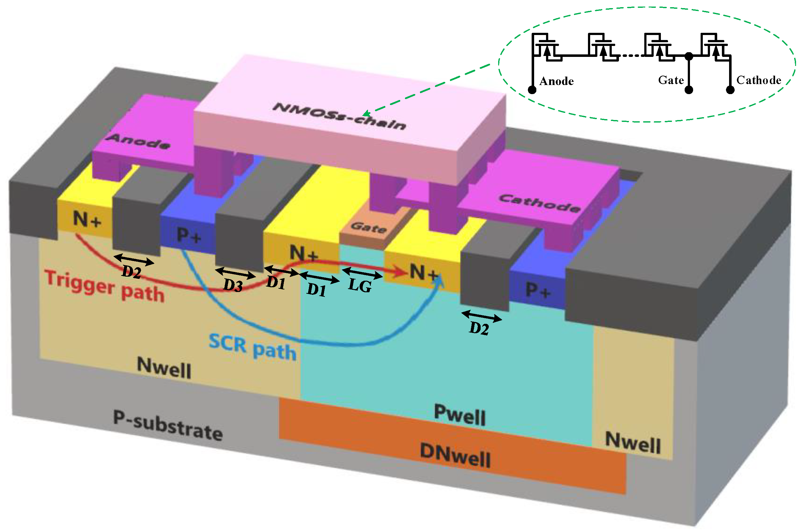
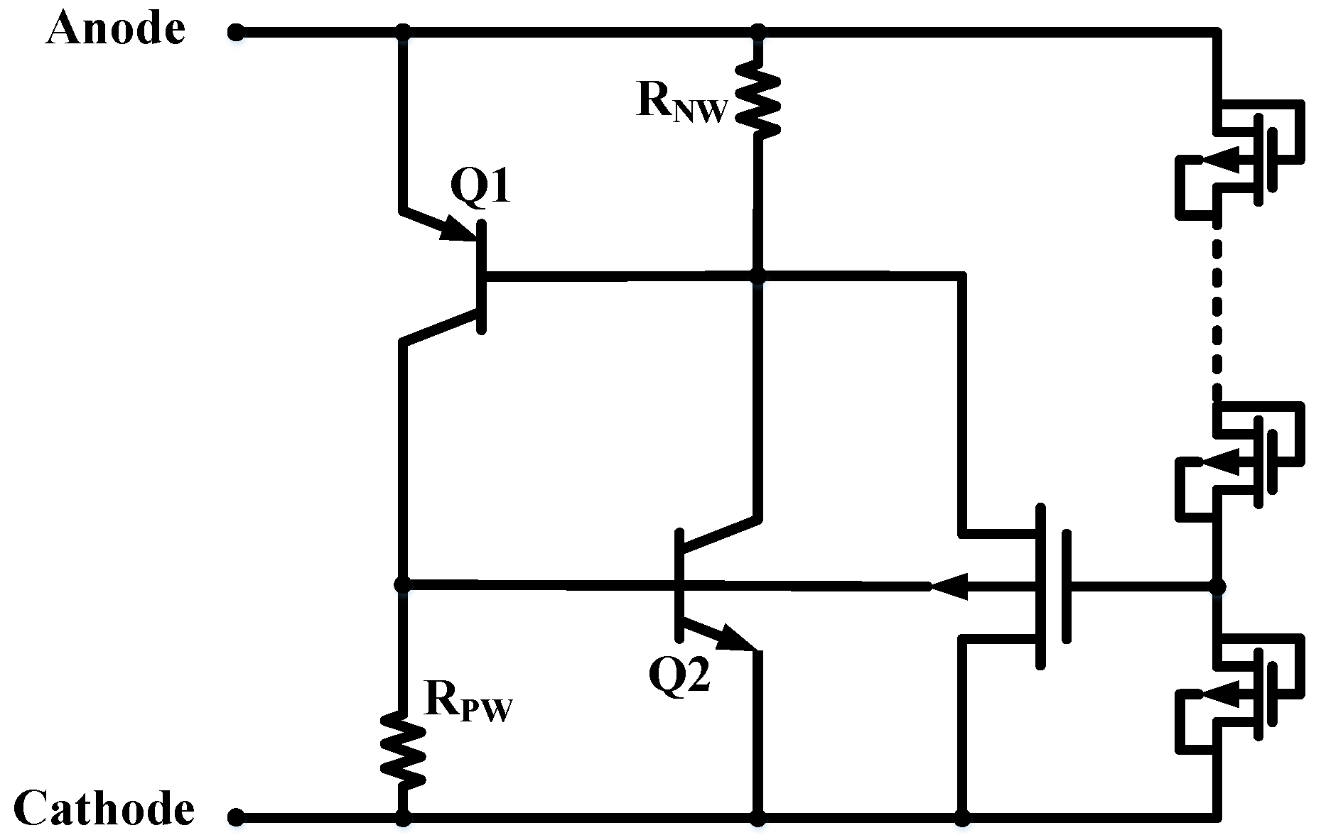
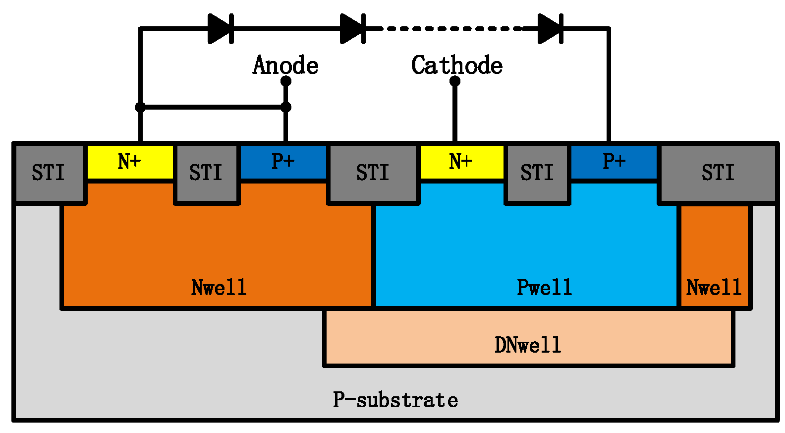
2. Mechanism
3. Results and Discussion
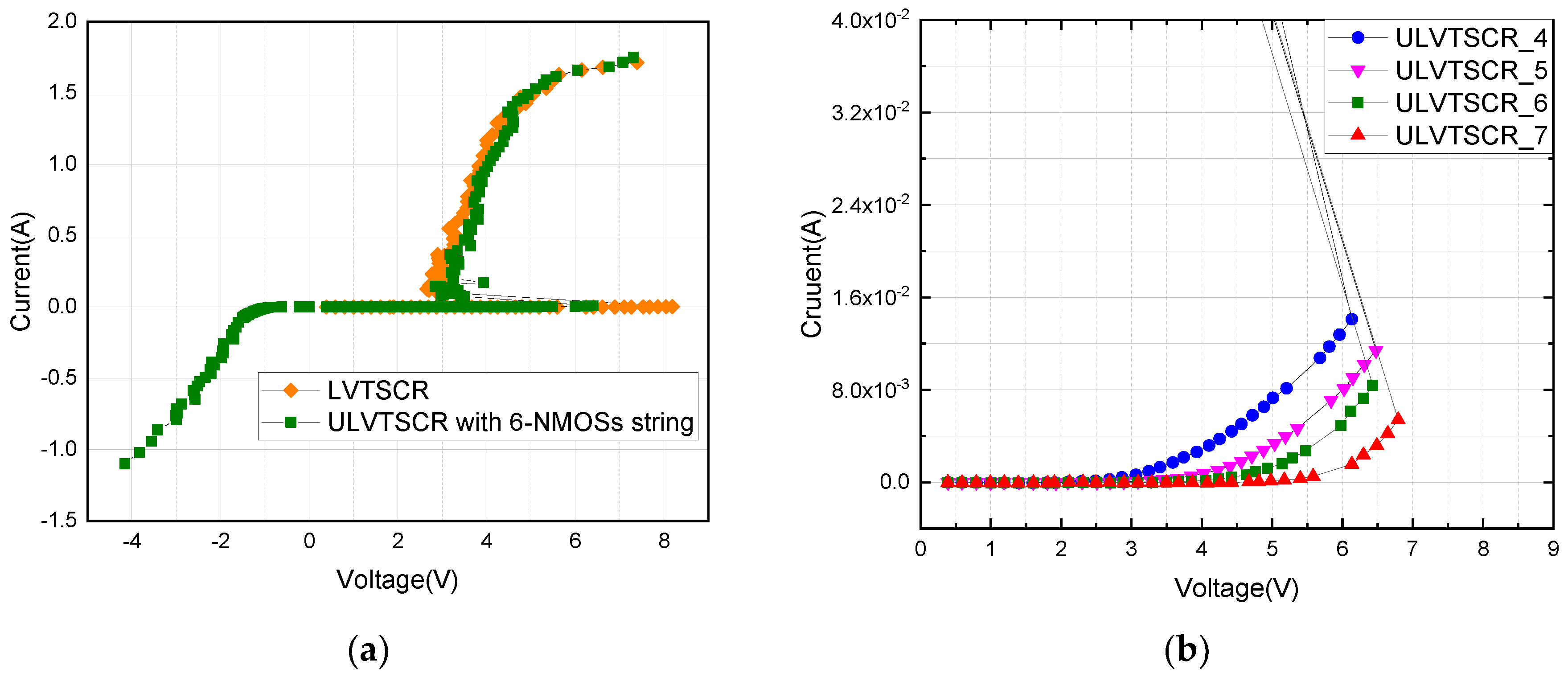
3.1. TLP Results
3.2. Overshoot
3.3. Leakage
4. Conclusions
Author Contributions
Funding
Data Availability Statement
Acknowledgments
Conflicts of Interest
References
- Wang, A.Z.; Feng, H.G.; Gong, K.; Zhan, R.Y.; Stine, J. On-chip ESD protection design for integrated circuits: An overview for IC designers. Microelectron. J. 2001, 32, 733–747. [Google Scholar] [CrossRef]
- Rountree, R.N.; Duvvury, C.; Maki, T. A process-tolerant input protection circuit for advanced CMOS process. In Proceedings of the EOS/ESD Symposium Proceedings, Reno, NV, USA, 4–8 October 1988; pp. 201–205. [Google Scholar]
- Rountree, R.N. ESD protection for submicron CMOS circuits-issues and solutions. In Proceedings of the Technical Digest., International Electron Devices Meeting, San Francisco, CA, USA, 11–14 December 1988; pp. 580–583. [Google Scholar]
- Chatterjee, A.; Polgreen, T. A low-voltage triggering SCR for on-chip ESD protection at output and input pads. In Proceedings of the IEEE Electron Device Papers, Honololu, HI, USA, 4–7 June 1990; Volume 12, pp. 75–76. [Google Scholar]
- Ker, M.D.; Hsu, K.C. Overview of on-chip electrostatic discharge protection design with SCR-based devices in CMOS integrated circuits. IEEE Trans. Device Mater. Reliab. 2005, 5, 235–249. [Google Scholar]
- Chen, L.; Du, F.; Chen, R.; Liu, J.; Liu, Z.; Zhang, L. Novel diode-triggered SCR with suppressed multiple triggering for ESD applications. In Proceedings of the 2018 IEEE International Conference on Electron Devices and Solid State Circuits (EDSSC), Shenzhen, China, 6–8 June 2018; pp. 1–2. [Google Scholar]
- Mergens, M. Speed optimized diode-triggered SCR (DTSCR) for RF ESD protection of ultra-sensitive IC nodes in advanced technologies. IEEE Trans. Device Mater 2005, 5, 532–542. [Google Scholar] [CrossRef]
- Yang, K.; Liu, J.; Liu, Z. LVTSCR with High Holding Voltage for ESD Protection in 55 nm CMOS Process. In Proceedings of the 2019 8th International Symposium on Next Generation Electronics (ISNE), Zhengzhou, China, 9–10 October 2019; pp. 1–3. [Google Scholar]
- Huang, M.; Du, F.; Hou, F.; Song, W.; Liu, J.; Liu, Z. Enhanced LVTSCR with High Holding Voltage in Advanced CMOS technology. In Proceedings of the 2019 IEEE International Conference on Electron Devices and Solid-State Circuits (EDSSC), Xi’an, China, 12–14 June 2019; pp. 1–2. [Google Scholar]
- Lin, C.-Y.; Wu, Y.-H.; Ker, M.-D. Low-Leakage and Low-Trigger-Voltage SCR Device for ESD Protection in 28-nm High-k Metal Gate CMOS Process. IEEE Electron Device Lett. 2016, 37, 1387–1390. [Google Scholar] [CrossRef]
- Galy, P.; Bourgeat, J.; Guitard, N.; Lise, J.D.; Marin-Cudraz, D.; Legrand, C.A. Ultracompact ESD Protection With BIMOS-Merged Dual Back-to-Back SCR in Hybrid Bulk 28-nm FD-SOI Advanced CMOS Technology. IEEE Trans. Electron Devices 2017, 64, 3991–3997. [Google Scholar] [CrossRef]
- Chen, W.Y.; Rosenbaum, E.; Ker, M.D. Diode-Triggered Silicon-Controlled Rectifier with Reduced Voltage Overshoot for CDM ESD Protection. IEEE Trans. Device Mater. Reliab. 2011, 12, 10–14. [Google Scholar] [CrossRef]
- Gauthier, R.; Abou-Khalil, M.; Chatty, K.; Mitra, S.; Li, J. Investigation of voltage overshoots in diode triggered silicon-controlled rectifiers (DTSCRs) under very fast transmission line pulsing (VFTLP). In Proceedings of the EOS/ESD Symposium, Anaheim, CA, USA, 30 August 2009–4 September 2009; pp. 334–343. [Google Scholar]


| W(μm) | D1 (μm) | D2 (μm) | D3 (μm) | LG (μm) |
|---|---|---|---|---|
| 40 | 0.5 | 2 | 0.5 | 0.3 |
| Device | D1 (μm) | Vh (V) | It2 (A) | It2 (mA/μm) |
|---|---|---|---|---|
| ULVTSCR-01 | 0.25 | 2.1 | 1.75 | 43 |
| ULVTSCR-02 | 0.50 | 3.0 | 1.68 | 42 |
| ULVTSCR-03 | 1.00 | 3.1 | 1.40 | 35 |
| ULVTSCR-04 | 2.00 | 4.2 | 1.00 | 25 |
| Device | Leakage (nA) | Leakage (nA/μm) |
|---|---|---|
| ULVTSCR-05@25 °C | 353 | 8.82 |
| ULVTSCR-06@25 °C | 25 | 0.62 |
| ULVTSCR-07@25 °C | 5 | 0.12 |
| ULVTSCR-05@125 °C | 4.78 (μA) | 120 |
| ULVTSCR-06@125 °C | 811 | 20.27 |
| ULVTSCR-07@125 °C | 241 | 6.02 |
Publisher’s Note: MDPI stays neutral with regard to jurisdictional claims in published maps and institutional affiliations. |
© 2022 by the authors. Licensee MDPI, Basel, Switzerland. This article is an open access article distributed under the terms and conditions of the Creative Commons Attribution (CC BY) license (https://creativecommons.org/licenses/by/4.0/).
Share and Cite
Chen, R.; Wei, H.; Liu, H.; Liu, Z.; Chen, Y. Ultra-Low-Voltage-Triggered Silicon Controlled Rectifier ESD Protection Device for 2.5 V Nano Integrated Circuit. Nanomaterials 2022, 12, 4250. https://doi.org/10.3390/nano12234250
Chen R, Wei H, Liu H, Liu Z, Chen Y. Ultra-Low-Voltage-Triggered Silicon Controlled Rectifier ESD Protection Device for 2.5 V Nano Integrated Circuit. Nanomaterials. 2022; 12(23):4250. https://doi.org/10.3390/nano12234250
Chicago/Turabian StyleChen, Ruibo, Hao Wei, Hongxia Liu, Zhiwei Liu, and Yaolin Chen. 2022. "Ultra-Low-Voltage-Triggered Silicon Controlled Rectifier ESD Protection Device for 2.5 V Nano Integrated Circuit" Nanomaterials 12, no. 23: 4250. https://doi.org/10.3390/nano12234250
APA StyleChen, R., Wei, H., Liu, H., Liu, Z., & Chen, Y. (2022). Ultra-Low-Voltage-Triggered Silicon Controlled Rectifier ESD Protection Device for 2.5 V Nano Integrated Circuit. Nanomaterials, 12(23), 4250. https://doi.org/10.3390/nano12234250