
Atom-to-Device Simulation of MoO3/Si Heterojunction Solar Cell

 ,
,  , ,
, , 
Abstract
1. Introduction
2. Materials and Methods
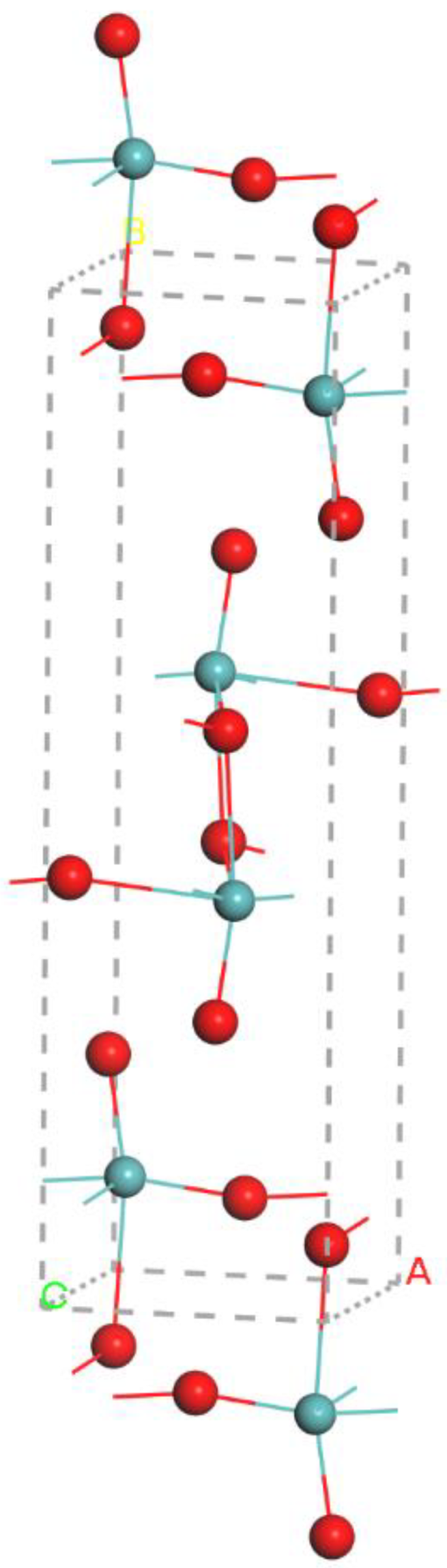
2.1. Method of Material Simulation
2.2. Method of Device Simulation
2.3. Theoretical Background of Device Simulation
3. Results and Discussion
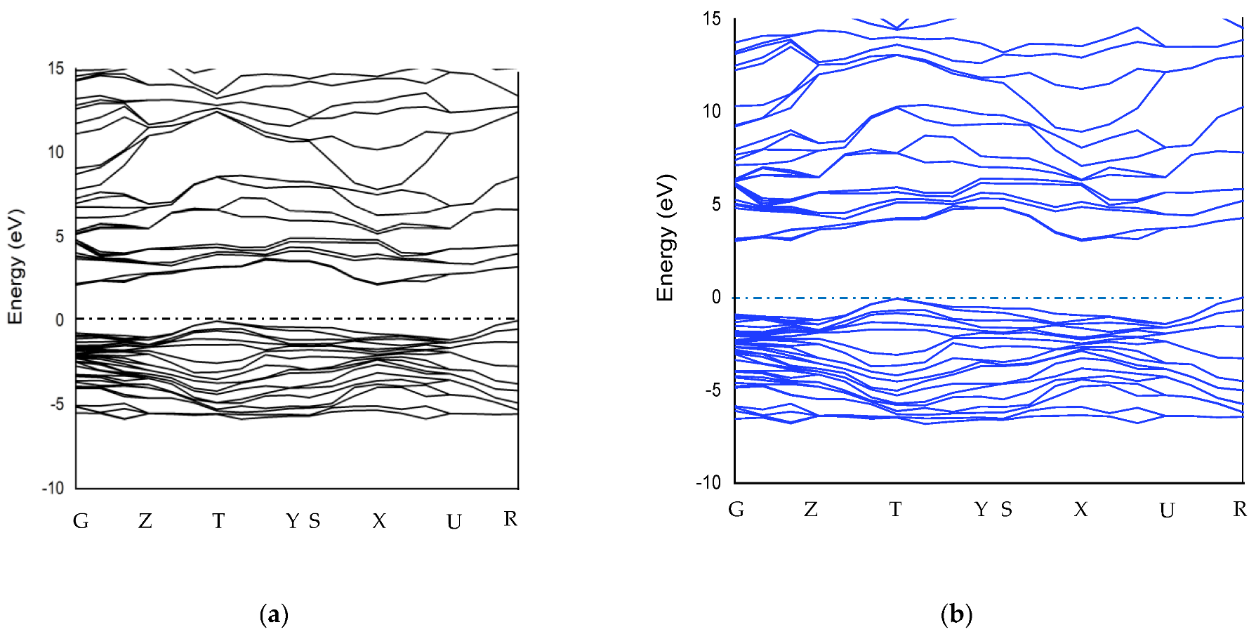
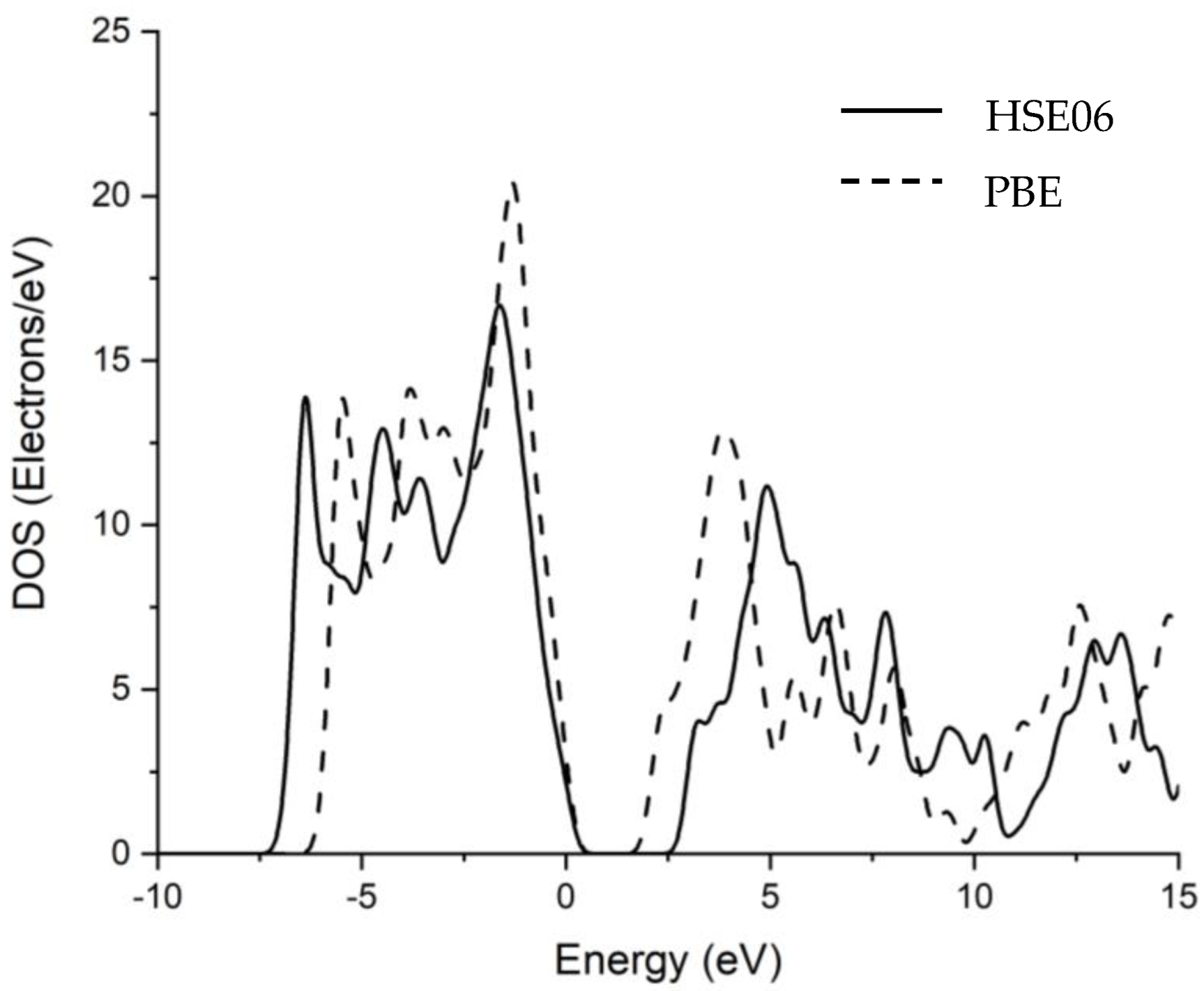
3.1. Band Structure
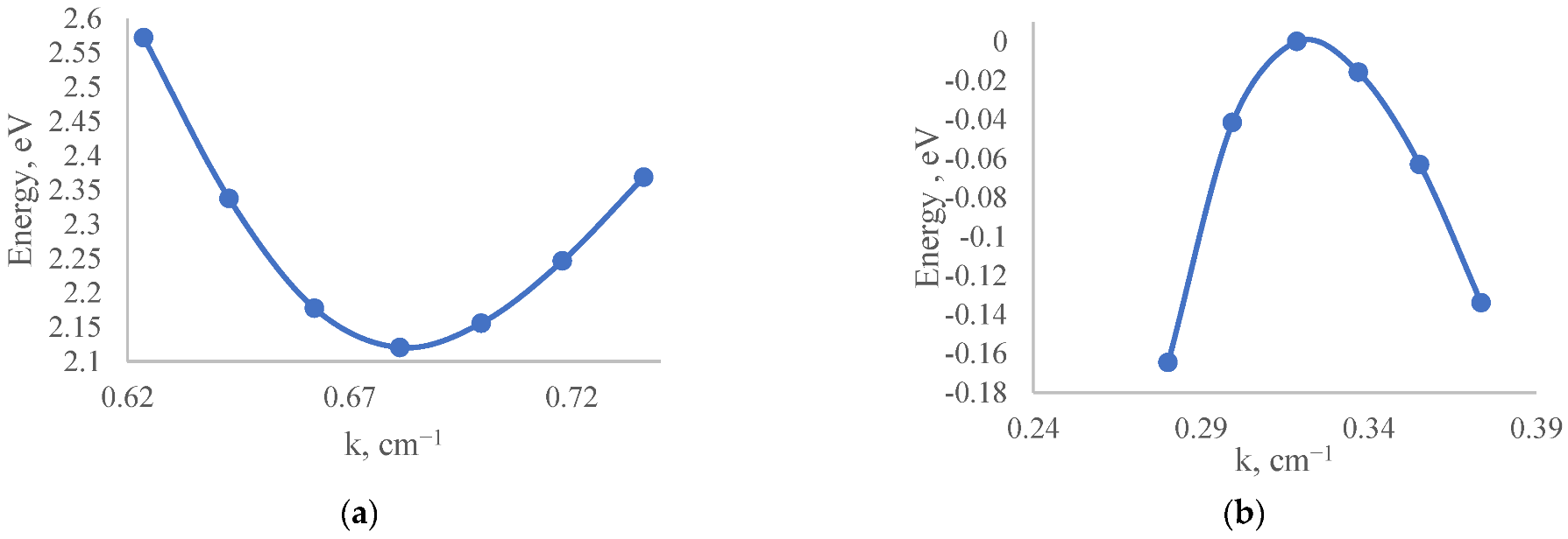
3.2. Effective Mass
3.3. Carriers Mobility
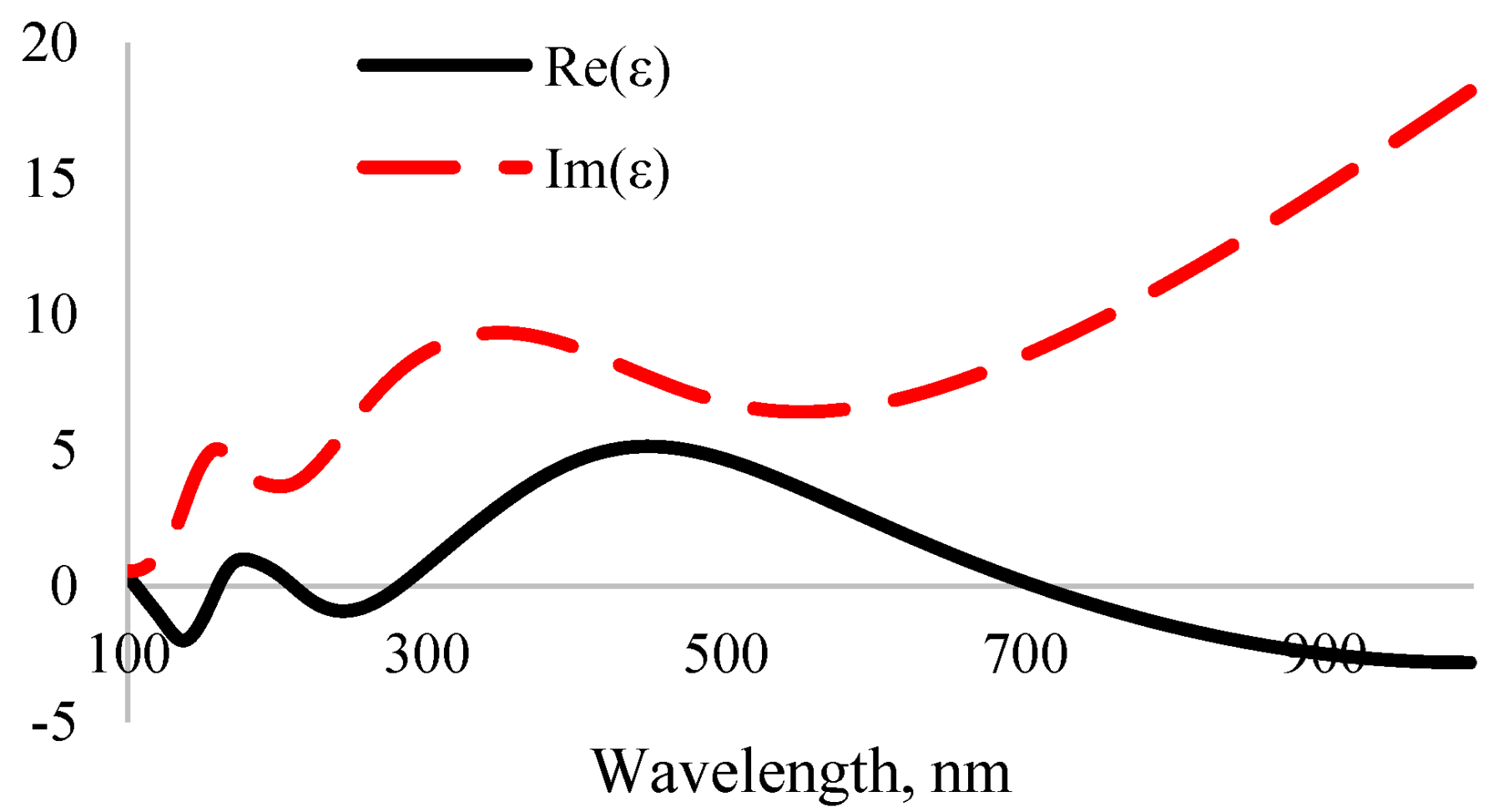
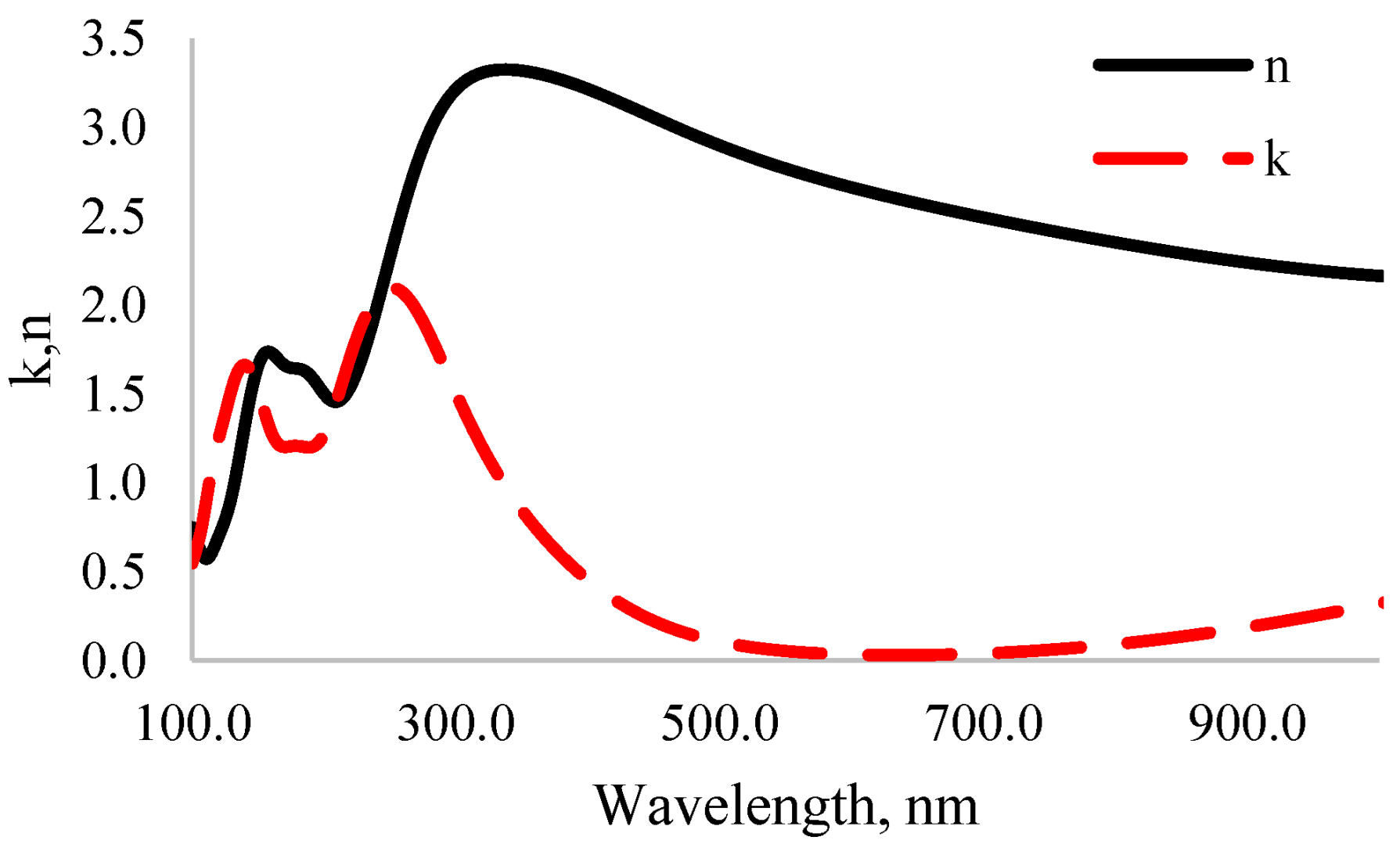
3.4. Optical Properties
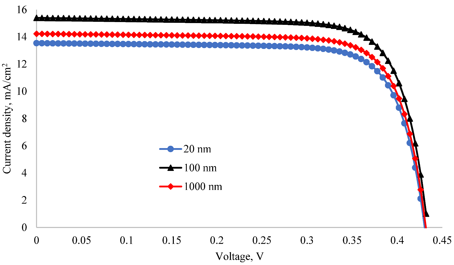
3.5. I-V Characteristics
4. Conclusions
Author Contributions
Funding
Institutional Review Board Statement
Informed Consent Statement
Data Availability Statement
Conflicts of Interest
References
- Franco, M.A.; Conti, P.P.; Andre, R.S.; Correa, D.S. A Review on Chemiresistive ZnO Gas Sensors. Sens. Actuators Rep. 2022, 4, 100100. [Google Scholar] [CrossRef]
- Park, H.; Alhammadi, S.; Reddy, V.; Reddy, M.; Park, C.; Kim, W.K. Influence of the Al-Doped ZnO Sputter-Deposition Temperature on Cu(In,Ga)Se2 Solar Cell Performance. Nanomaterials 2022, 12, 3326. [Google Scholar] [CrossRef] [PubMed]
- Parashar, M.; Shukla, V.K.; Singh, R. Metal Oxides Nanoparticles via Sol–Gel Method: A Review on Synthesis, Characterization and Applications. J. Mater. Sci. Mater. Electron. 2020, 31, 3729–3749. [Google Scholar] [CrossRef]
- Nguyen, T.T.; Patel, M.; Kim, J. All-Inorganic Metal Oxide Transparent Solar Cells. Sol. Energy Mater. Sol. Cells 2020, 217, 110708. [Google Scholar] [CrossRef]
- Nguyen, T.T.; Patel, M.; Kim, S.; Mir, R.A.; Yi, J.; Dao, V.A.; Kim, J. Transparent Photovoltaic Cells and Self-Powered Photodetectors by TiO2/NiO Heterojunction. J. Power Sources 2021, 481, 228865. [Google Scholar] [CrossRef]
- Sagar, R.; Rao, A. Increasing the Silicon Solar Cell Efficiency with Transition Metal Oxide Nano-Thin Films as Anti-Reflection Coatings. Mater. Res. Express 2020, 7, 016433. [Google Scholar] [CrossRef]
- Yang, J.; Zhang, Q.; Xu, J.; Liu, H.; Qin, R.; Zhai, H.; Chen, S.; Yuan, M. All-Inorganic Perovskite Solar Cells Based on CsPbIBr2 and Metal Oxide Transport Layers with Improved Stability. Nanomaterials 2019, 9, 1666. [Google Scholar] [CrossRef]
- Hodes, G. Perovskite-Based Solar Cells. Science 2013, 342, 317–318. [Google Scholar] [CrossRef]
- Wang, C.; Su, Z.; Chen, L.; Zhang, H.; Hui, W.; Liang, D.; Zheng, G.; Zhang, L.; Tang, Z.; Wen, W.; et al. MoO3 Doped PTAA for High-Performance Inverted Perovskite Solar Cells. Appl. Surf. Sci. 2022, 571, 151301. [Google Scholar] [CrossRef]
- Babu Reddy, L.P.; Rajprakash, H.G.; Ravikiran, Y.T. Synthesis of α-MoO3 Nanorods by Sol Gel Synthesis and to Investigate Its Room Temperature Humidity Sensing Properties. AIP Conf. Proc. 2019, 2142, 070022. [Google Scholar] [CrossRef]
- Bhatia, S.; Khanna, A. Structural and Optical Properties of Molybdenum Trioxide Thin Films. AIP Conf. Proc. 2015, 1665, 080057. [Google Scholar] [CrossRef]
- Lei, Z.; Yang, X.; Dong, J.; Yi, X. Novel Metastable Hexagonal MoO3 Nanobelts: Synthesis, Photochromic, and Electrochromic Properties. Chem. Mater. 2009, 21, 5681–5690. [Google Scholar] [CrossRef]
- Kumar, V.; Wang, X.; Lee, P.S. Oxygen-Ions-Mediated Pseudocapacitive Charge Storage in Molybdenum Trioxide Nanobelts. ChemNanoMat 2015, 1, 403–408. [Google Scholar] [CrossRef]
- Brezesinski, T.; Wang, J.; Tolbert, S.H.; Dunn, B. Ordered Mesoporous α-MoO3 with Iso-Oriented Nanocrystalline Walls for Thin-Film Pseudocapacitors. Nat. Mater. 2010, 9, 146–151. [Google Scholar] [CrossRef]
- Lupan, O.; Cretu, V.; Deng, M.; Gedamu, D.; Paulowicz, I.; Kaps, S.; Mishra, Y.K.; Polonskyi, O.; Zamponi, C.; Kienle, L.; et al. Versatile Growth of Freestanding Orthorhombic α-Molybdenum Trioxide Nano- and Microstructures by Rapid Thermal Processing for Gas Nanosensors. J. Phys. Chem. C 2014, 118, 15068–15078. [Google Scholar] [CrossRef]
- Girotto, C.; Voroshazi, E.; Cheyns, D.; Heremans, P.; Rand, B.P. Solution-Processed MoO3 Thin Films as a Hole-Injection Layer for Organic Solar Cells. ACS Appl. Mater. Interfaces 2011, 3, 3244–3247. [Google Scholar] [CrossRef]
- Ballif, C.; Haug, F.J.; Boccard, M.; Verlinden, P.J.; Hahn, G. Status and Perspectives of Crystalline Silicon Photovoltaics in Research and Industry. Nat. Rev. Mater. 2022, 7, 597–616. [Google Scholar] [CrossRef]
- Ho, W.J.; Liu, J.J.; Yang, Y.C.; Ho, C.H. Enhancing Output Power of Textured Silicon Solar Cells by Embedding Indium Plasmonic Nanoparticles in Layers within Antireflective Coating. Nanomaterials 2018, 8, 1003. [Google Scholar] [CrossRef]
- Gulomov, J.; Aliev, R. Influence of the Angle of Incident Light on the Performance of Textured Silicon Solar Cells. J. Nano-Electron. Phys. 2021, 13, 06036. [Google Scholar] [CrossRef]
- Gulomov, J.; Aliev, R. Study of the Temperature Coefficient of the Main Photoelectric Parameters of Silicon Solar Cells with Various Nanoparticles. J. Nano-Electron. Phys. 2021, 13, 04033. [Google Scholar] [CrossRef]
- Luo, Z.; Guo, T.; Wang, C.; Zou, J.; Wang, J.; Dong, W.; Li, J.; Zhang, W.; Zhang, X.; Zheng, W. Enhancing the Efficiency of Perovskite Solar Cells through Interface Engineering with MoS2 Quantum Dots. Nanomaterials 2022, 12, 3079. [Google Scholar] [CrossRef] [PubMed]
- Ehrler, B.; Alarcón-Lladó, E.; Tabernig, S.W.; Veeken, T.; Garnett, E.C.; Polman, A. Photovoltaics Reaching for the Shockley-Queisser Limit. ACS Energy Lett. 2020, 5, 3029–3033. [Google Scholar] [CrossRef]
- Fernández, S.; Torres, I.; Gandía, J.J. Sputtered Ultrathin TiO2 as Electron Transport Layer in Silicon Heterojunction Solar Cell Technology. Nanomaterials 2022, 12, 2441. [Google Scholar] [CrossRef] [PubMed]
- Gulomov, J.; Accouche, O.; Aliev, R.; AZAB, M.; Gulomova, I. Analyzing the ZnO and CH3NH3PbI3 as Emitter Layer for Silicon Based Heterojunction Solar Cells. Comput. Mater. Contin. 2022, 74, 575–590. [Google Scholar] [CrossRef]
- Clark, S.J.; Segall, M.D.; Pickard, C.J.; Hasnip, P.J.; Probert, M.I.J.; Refson, K.; Payne, M.C. First Principles Methods Using CASTEP. Z. Fur Krist. 2005, 220, 567–570. [Google Scholar] [CrossRef]
- Koelling, D.D.; Harmon, B.N. A Technique for Relativistic Spin-Polarised Calculations. J. Phys. C Solid State Phys. 1977, 10, 3107. [Google Scholar] [CrossRef]
- Pfrommer, B.G.; Côté, M.; Louie, S.G.; Cohen, M.L. Relaxation of Crystals with the Quasi-Newton Method. J. Comput. Phys. 1997, 131, 233–240. [Google Scholar] [CrossRef]
- Ernzerhof, M.; Scuseria, G.E. Assessment of the Perdew–Burke–Ernzerhof Exchange-Correlation Functional. J. Chem. Phys. 1999, 110, 5029. [Google Scholar] [CrossRef]
- Heyd, J.; Scuseria, G.E.; Ernzerhof, M. Hybrid Functionals Based on a Screened Coulomb Potential. J. Chem. Phys. 2003, 118, 8207, Erratum in J. Chem. Phys. 2006, 124, 219906. [Google Scholar] [CrossRef]
- Liu, X.; Zhu, X.; Wang, C.; Cao, Y.; Wang, B.; Ou, H.; Wu, Y.; Mei, Q.; Zhang, J.; Cong, Z.; et al. Silicon-Based Metastructure Optical Scattering Multiply–Accumulate Computation Chip. Nanomaterials 2022, 12, 2136. [Google Scholar] [CrossRef]
- Belarbi, M.; Beghdad, M.; Mekemeche, A. Simulation and Optimization of N-Type Interdigitated Back Contact Silicon Heterojunction (IBC-SiHJ) Solar Cell Structure Using Silvaco Tcad Atlas. Sol. Energy 2016, 127, 206–215. [Google Scholar] [CrossRef]
- Gulomov, J.; Aliev, R. Analyzing Periodical Textured Silicon Solar Cells by the TCAD Modeling. Sci. Tech. J. Inf. Technol. Mech. Opt. 2021, 21, 626–632. [Google Scholar] [CrossRef]
- Peelaers, H.; Chabinyc, M.L.; van de Walle, C.G. Controlling N-Type Doping in MoO3. Chem. Mater. 2017, 29, 2563–2567. [Google Scholar] [CrossRef]
- Gulomov, J.; Aliev, R.; Urmanov, B. Effect of the Thickness on Photoelectric Parameters of a Textured Silicon Solar Cell. J. Surf. Investig. X-ray Synchrotron Neutron Tech. 2022, 16, 416–420. [Google Scholar] [CrossRef]
- Gulomov, J.; Aliev, R. Numerical Analysis of the Effect of Illumination Intensity on Photoelectric Parameters of the Silicon Solar Cell with Various Metal Nanoparticles. Nanosyst. Phys. Chem. Math. 2021, 12, 569–574. [Google Scholar] [CrossRef]
- Yevick, D.; Friese, T.; Schmidt, F. A Comparison of Transparent Boundary Conditions for the Fresnel Equation. J. Comput. Phys. 2001, 168, 433–444. [Google Scholar] [CrossRef]
- Gulomov, J.; Accouche, O.; Aliev, R.; Neji, B.; Ghandour, R.; Gulomova, I.; Azab, M. Geometric Optimization of Perovskite Solar Cells with Metal Oxide Charge Transport Layers. Nanomaterials 2022, 12, 2692. [Google Scholar] [CrossRef]
- Jäger, K.; van Swaaij, R.A.C.M.M.; Zeman, M. The Scalar Scattering Theory: A Multi-Functional Tool for Optimizing Scattering in Thin-Film Silicon Solar Cells. In Renewable Energy and the Environment Optics and Photonics Congress (2012); paper PT3C.7; Optica Publishing Group: Washington, DC, USA, 2012. [Google Scholar] [CrossRef]
- Escarré, J.; Villar, F.; Asensi, J.M.; Bertomeu, J.; Andreu, J. Spectral Analysis of the Angular Distribution Function of Back Reflectors for Thin Film Silicon Solar Cells. J. Non-Cryst. Solids 2006, 352, 1896–1899. [Google Scholar] [CrossRef][Green Version]
- Abduvohidov, M.K.; Aliev, R.; Gulomov, J. A Study of the Influence of the Base Thickness on Photoelectric Parameterof Silicon Solar Cells with the New TCAD Algorithms. Sci. Tech. J. Inf. Technol. Mech. Opt. 2021, 21, 774–784. [Google Scholar] [CrossRef]
- Lowney, J.R.; Larrabee, R.D. The Use of Fick’s Law in Modeling Diffusion Processes. IEEE Trans Electron Devices 1980, 27, 1795–1798. [Google Scholar] [CrossRef]
- Sayede, A.D.; Amriou, T.; Pernisek, M.; Khelifa, B.; Mathieu, C. An Ab Initio LAPW Study of the α and β Phases of Bulk Molybdenum Trioxide, MoO3. Chem. Phys. 2005, 316, 72–82. [Google Scholar] [CrossRef]
- Scanlon, D.O.; Watson, G.W.; Payne, D.J.; Atkinson, G.R.; Egdell, R.G.; Law, D.S.L. Theoretical and Experimental Study of the Electronic Structures of MoO3 and MoO2. J. Phys. Chem. C 2010, 114, 4636–4645. [Google Scholar] [CrossRef]
- Xie, Y.; Kent, P.R.C. Hybrid Density Functional Study of Structural and Electronic Properties of Functionalized Tin+1Xn (X=C, N) Monolayers. Phys. Rev. B Condens. Matter Mater. Phys. 2013, 87, 235441. [Google Scholar] [CrossRef]
- Carcia, P.F.; McCarron, E.M. Synthesis and Properties of Thin Film Polymorphs of Molybdenum Trioxide. Thin Solid Film. 1987, 155, 53–63. [Google Scholar] [CrossRef]
- Qu, Q.; Zhang, W.B.; Huang, K.; Chen, H.M. Electronic Structure, Optical Properties and Band Edges of Layered MoO3: A First-Principles Investigation. Comput. Mater. Sci. 2017, 130, 242–248. [Google Scholar] [CrossRef]
- Dandogbessi, B.S.; Akin-Ojo, O. First Principles Prediction of the Electronic Structure and Carrier Mobilities of Biaxially Strained Molybdenum Trioxide (MoO3). J. Appl. Phys. 2016, 120, 055105. [Google Scholar] [CrossRef]
- Rostampour, E. Effect of Position-Dependent Effective Mass on Electron Tunneling of InAs/GaSb Type-II Superlattice Having Triangular and Parabolic Geometries. Opt. Laser Technol. 2021, 138, 106840. [Google Scholar] [CrossRef]
- Faghaninia, A.; Ager, J.W.; Lo, C.S. Ab Initio Electronic Transport Model with Explicit Solution to the Linearized Boltzmann Transport Equation. Phys. Rev. B Condens. Matter Mater. Phys. 2015, 91, 235123. [Google Scholar] [CrossRef]
- Bardeen, J.; Shockley, W. Deformation Potentials and Mobilities in Non-Polar Crystals. Phys. Rev. 1950, 80, 72. [Google Scholar] [CrossRef]
- Xi, J.; Long, M.; Tang, L.; Wang, D.; Shuai, Z. First-Principles Prediction of Charge Mobility in Carbon and Organic Nanomaterials. Nanoscale 2012, 4, 4348–4369. [Google Scholar] [CrossRef]
- Kamiya, M.; Sekino, H.; Tsuneda, T.; Hirao, K. Nonlinear Optical Property Calculations by the Long-Range-Corrected Coupled-Perturbed Kohn–Sham Method. J. Chem. Phys. 2005, 122, 234111. [Google Scholar] [CrossRef]
- Mocci, P.; Malloci, G.; Bosin, A.; Cappellini, G. Time-Dependent Density Functional Theory Investigation on the Electronic and Optical Properties of Poly-C,Si,Ge-Acenes. ACS Omega 2020, 5, 16654–16663. [Google Scholar] [CrossRef]
- Bakry, M.; Klinkenbusch, L. Using The Kramers-Kronig Transforms To Retrieve The Conductivity From The Effective Complex Permittivity. Adv. Radio Sci. 2018, 16, 23–28. [Google Scholar] [CrossRef]
- Ramanavicius, S.; Ramanavicius, A. Insights in the Application of Stoichiometric and Non-Stoichiometric Titanium Oxides for the Design of Sensors for the Determination of Gases and VOCs (TiO2−x and TinO2n−1 vs. TiO2). Sensors 2020, 20, 6833. [Google Scholar] [CrossRef]
- Aspnes, D.E.; Studna, A.A. Dielectric Functions and Optical Parameters of Si, Ge, GaP, GaAs, GaSb, InP, InAs, and InSb from 1.5 to 6.0 EV. Phys. Rev. B 1983, 27, 985. [Google Scholar] [CrossRef]
- Hass, G.; Cox, J.T. Antireflection Coatings for Germanium and Silicon in the Infrared. J. Opt. Soc. Am. 1958, 48, 677–680. [Google Scholar] [CrossRef]
- Jhou, J.C.; Gaurav, A.; Chang, C.H.; Lin, C.F. Enhanced Efficiency of Semitransparent Perovskite Solar Cells via Double-Sided Sandwich Evaporation Technique for Four Terminal Perovskite-Silicon Tandem Application. Nanomaterials 2022, 12, 1569. [Google Scholar] [CrossRef]


Publisher’s Note: MDPI stays neutral with regard to jurisdictional claims in published maps and institutional affiliations. |
© 2022 by the authors. Licensee MDPI, Basel, Switzerland. This article is an open access article distributed under the terms and conditions of the Creative Commons Attribution (CC BY) license (https://creativecommons.org/licenses/by/4.0/).
Share and Cite
Gulomov, J.; Accouche, O.; Al Barakeh, Z.; Aliev, R.; Gulomova, I.; Neji, B. Atom-to-Device Simulation of MoO3/Si Heterojunction Solar Cell. Nanomaterials 2022, 12, 4240. https://doi.org/10.3390/nano12234240
Gulomov J, Accouche O, Al Barakeh Z, Aliev R, Gulomova I, Neji B. Atom-to-Device Simulation of MoO3/Si Heterojunction Solar Cell. Nanomaterials. 2022; 12(23):4240. https://doi.org/10.3390/nano12234240
Chicago/Turabian StyleGulomov, Jasurbek, Oussama Accouche, Zaher Al Barakeh, Rayimjon Aliev, Irodakhon Gulomova, and Bilel Neji. 2022. "Atom-to-Device Simulation of MoO3/Si Heterojunction Solar Cell" Nanomaterials 12, no. 23: 4240. https://doi.org/10.3390/nano12234240
APA StyleGulomov, J., Accouche, O., Al Barakeh, Z., Aliev, R., Gulomova, I., & Neji, B. (2022). Atom-to-Device Simulation of MoO3/Si Heterojunction Solar Cell. Nanomaterials, 12(23), 4240. https://doi.org/10.3390/nano12234240