Article

Heterostructures of Cut Carbon Nanotube-Filled Array of TiO2 Nanotubes for New Module of Photovoltaic Devices

1
Institute of Hybrid Materials, National Center of International Joint Research for Hybrid Materials Technology, National Base of International Sci. & Tech. Cooperation on Hybrid Materials, Qingdao University, 308 Ningxia Road, Qingdao 266071, China
2
V.I. Vernadskii Institute of General and Inorganic Chemistry of the Ukrainian NAS, 32/34 Palladin avenue, 03142 Kyiv, Ukraine
3
Department of Mechanical Engineering, Colorado State University, Fort Collins, CO 80523, USA
4
Department of Chemical and Biological Engineering, Colorado State University, Fort Collins, CO 80523, USA
*
Authors to whom correspondence should be addressed.
Nanomaterials 2022, 12(20), 3604; https://doi.org/10.3390/nano12203604
Submission received: 10 August 2022 / Revised: 24 September 2022 / Accepted: 11 October 2022 / Published: 14 October 2022
(This article belongs to the Section Nanophotonics Materials and Devices)

Abstract

:
In this work, a new photovoltaic device was prepared. The device uses titanium (Ti) foil/TiO2 nanotubes as the photoanode and multi-walled carbon nanotubes (MWCNTs) as a photosensitizer. Titanium dioxide nanotube arrays (TiO2-NTs) were prepared by one-step anodic oxidation. Cut-MWCNTs with a length of less than 100 nm were obtained by the mixed-acid oxidation of MWCNTs. The two materials were combined to form a TiO2-NTs@cut-MWCNT heterostructure by electrophoresis. TiO2-NTs@cut-MWCNTs were characterized by field-emission scanning electron microscopy (FESEM) and X-ray diffraction (XRD), which showed that the two materials were effectively combined. We fabricated the heterostructure into a photovoltaic device, showing an enhanced photocurrent response and an efficiency of 0.0138%, and explained this phenomenon by performing UV-vis absorption spectroscopy and electrochemical tests. It is hoped that this work can provide a reference value for the application of carbon nanotubes in photovoltaic devices.

1. Introduction

Solar energy is renewable energy with the advantages of wide distribution, easy access, and inexhaustible supply. As an effective way to utilize solar energy, solar cells have always been a research hotspot [1]. Silicon-based solar cells are the most mature at present, but they are expensive, consume lots of energy in the production process, and have a long cost recovery period, which are all barriers to their large-scale application and promotion. In 1986, Dr. C.W. Tang [2] first prepared a double-layer organic solar cell device with copper titanate cyanine as the donor material and perylene as the acceptor material and tested it under simulated sunlight to obtain an efficiency of 1%. In 1991, O’Regan and Grätzel [3] manufactured the first nanocrystalline TiO2 chemical solar cell. Compared with traditional solar cells, this cell has the advantages of a simple manufacturing process, low production cost, and non-toxic and pollution-free production, and it is expected to compete with silicon technology in the future [4]. In contrast, the light-absorbing layer materials of dye-sensitized solar cells and polymer solar cells need to undergo complex organic synthesis, and their stability is not high. Therefore, researchers have been exploring new materials, new processes, and new structures.
TiO2 is an excellent candidate semiconductor material for the effective use of solar energy because of its appropriate band gap, low cost, good chemical stability, and photostability. Since Grimes et al. [5] first reported the successful preparation of highly ordered TiO2 nanotube arrays (TiO2-NTs) by electrochemical anodization, the synthesis and application of one-dimensional tubular array structures represented by TiO2-NTs have increased rapidly. This structural material has a high orientation, can provide a good path for electron transfer, and is simple to manufacture. Its preparation avoids the cumbersome process of organic synthesis, provides the possibility for large-scale roll-to-roll production, and is proven to have great application value in photovoltaic devices [6,7,8,9,10,11].
Although TiO2 has high photoactivity among many oxide semiconductors, its ability to use sunlight is still very limited, and the recombination rate of photogenerated charges is high, resulting in low quantum yield. Therefore, a lot of work has been conducted to develop modifications of TiO2. Carbon nanotubes are cheap and easy to obtain by chemical treatment. Their energy-level position and band-gap width can be changed to match the energy level of TiO2. They can therefore be used as a photosensitizer “dye”. Multi-walled carbon nanotubes (MWCNTs) are composed of multiple single-walled carbon nanotubes (SWCNTs). The density of states of each single-walled carbon nanotube has Van Hove singularity and exhibits a photovoltaic effect. Therefore, they have attracted great attention in the field of photoelectrochemistry [12,13,14,15,16,17,18,19]. Kumar and colleagues [20] used TiO2 and MWCNTs as active charge-generating layers by spin-coating them on transparent conductive substrates to fabricate solar cells. The efficiency of the TiO2@MWCNT solar cell was 0.4%. Kalitag et al. [21] embedded cut MWCNTs into polymer films to improve their performance and found that cut MWCNTs have better hole transport ability. Baker et al. [22] reviewed carbon solar cells, which use carbon nanotubes as the photosensitive layer with semiconductor properties.
In this work, we propose an all-titanium–carbon photovoltaic device. TiO2-NTs were first prepared by anodization, cut-MWCNTs were prepared by mixed-acid oxidation, and then the two materials were combined to form a TiO2-NTs@cut-MWCNT heterostructure by a simple electrophoresis method [23]. Although the heterostructure formed by the composite of TiO2 and carbon nanotubes has been applied in the field of photocatalysis, its functional mechanism for light energy conversion has not yet been reported [24,25,26], and there is no example of fabricating photovoltaic devices using only TiO2 and carbon nanotubes. Therefore, we prepared an all-titanium–carbon photovoltaic device based on the TiO2-NTs@cut-MWCNT heterostructure. The charge-transfer mechanism in the device was studied by electrochemical tests. Most importantly, the material cost of the photovoltaic device is low, and the experimental method is simple. We hope this work can provide some reference value for the application of carbon nanotubes in photovoltaic devices.

2. Materials and Methods

2.1. Fabrication of TiO2-NTs

Pure Ti foil (150 µm thick, 99.99%) was sanded and then ultrasonically cleaned with isopropanol, ethanol, and deionized water for 10 min each. The natural surface oxides were then removed with hydrochloric acid (HCl:H2O = 1:1) [27]. The cleaned foils were stored in DI water for later use. Pt foil (100 µm thick, 99.9%) was used as the counter electrode. The electrolyte solution was 95 vol% diethylene glycol (DEG), 2 vol% HF, and 3 vol% DI water. Highly ordered TiO2-NTs were prepared by electrochemical anodization at 55 V for 1 h at room temperature. After anodization, the anodized TiO2 nanotube array samples were rinsed in isopropanol and DI water to remove the electrolyte and dried in a fume hood, followed by annealing at 530 °C for 3 h in an air atmosphere to obtain the crystal structure.

2.2. Cutting of the MWCNTs

MWCNTs (purity > 95%; length: 0.5–2 μm) were purchased from Macklin. The cutting steps are as follows: 100 mg of MWCNTs was placed in 30 mL of concentrated H2SO4 and stirred at room temperature for 30 min to obtain a uniform suspension. The suspension was then mixed with 18 mL of concentrated HNO3 and heated and stirred at 70~80 °C for 10 h. The cut carbon nanotubes were collected by centrifugation and washed repeatedly with DI water until the pH value reached neutrality.

2.3. Preparation of the Heterostructure of TiO2-NTs@cut-MWCNTs

The heterostructure of TiO2-NTs@cut-MWCNTs was formed by electrophoresis. Cut-MWCNTs were dispersed in deionized water and then sonicated to form a homogeneous suspension. The as-prepared TiO2-NTs were used as substrates. In the cut-MWCNT suspension, Pt foil used as the counter electrode was kept 1 cm parallel to the TiO2 electrode. Figure S1 is a schematic diagram of the electrophoresis device using an RPS6005C-2DC stabilized power supply. When a forward voltage was applied, the negatively charged cut-MWCNTs in the solution moved directionally into the TiO2-NTs under the action of the electric field. When a reverse voltage was applied, part of the cut-MWCNTs in the suspension reoriented and moved. When the forward voltage was reapplied, the moving direction of the cut-MWCNTs changed again. Alternating the sign of the voltage many times could improve the contact between cut-MWCNTs and TiO2-NTs. The electrophoresis voltage was 20 V, the forward voltage was applied for 30 s, and the reverse voltage was applied for 5 s; this cycle was repeated 30 times. Finally, the samples were rinsed with deionized water 3 times and dried overnight at 60 °C.

2.4. Fabrication of All-Titanium–Carbon Photovoltaic Device

The photovoltaic device is mainly composed of carbon nanotubes and TiO2, so it is called an “all-titanium–carbon photovoltaic device”. The preparation process of the device is as follows: (1) Preparation of the photoanode: The prepared TiO2-NTs@cut-MWCNT heterostructure was used as the photoanode. (2) Preparation of the counter electrode: In order to avoid the short circuit of the direct contact between TiO2-NTs and ITO inside the device, ITO spin-coated with a small amount of cut-MWCNTs was used as the counter electrode. (3) Preparation of electrolyte: The electrolyte was a 0.2 M K3[Fe(CN)6]/K4[Fe(CN)6] aqueous solution. (4) Assembly of the device: The photoanode was placed in the sealed insulating groove and covered with the counter electrode, the electrodes were staggered and clamped with clips, and the electrolyte was injected from the edge. In order to avoid an internal short circuit, a few droplets were used to test the efficiency. The experimental process and device structure are shown in Figure 1.

2.5. Characterization

MWCNTs and cut-MWCNTs were characterized by TEM, FESEM, Raman, FT-IR, XRD, BET surface analysis, and XPS. TEM images were obtained with a Thermo Scientific F200i (USA) transmission electron microscope. FESEM images were obtained with a Regulus 8100. The Raman spectra were obtained using an Almega Thermo Nicolet Dispersion Raman spectrometer (laser wavelength: 532 nm). Fourier transform infrared spectroscopy (FT-IR) data were measured using a Nicolet 6700 Fourier transform infrared spectrometer from Thermo Corporation (Waltham, MA, USA). XRD was performed with a Bruker D8 Advance model. BET surface analysis was measured using Micromeritics ASAP 2460. XPS data were measured using the Thermo Scientific K-Alpha Spectrometer (USA). Optical properties were characterized by a UV-vis spectrometer (Lambda 750s) with a wavelength range of 200 to 800 nm.
TiO2-NTs and TiO2-NTs@cut-MWCNTs were analyzed by FESEM, UV-vis, and XRD. FESEM images were obtained on a Hitachi-SU8220 at an accelerating voltage of 20 kV without gold plating. The spectral absorptions of TiO2-NTs and TiO2-NTs@cut-MWCNTs were obtained using PerkinElmer Lambda 750s with an integrating sphere. The crystal structures of the surface were analyzed by X-ray diffraction (XRD) using a Bruker D8 Advance diffractometer (Co Kα radiation, λ = 1.54056 nm).

3. Results and Discussion

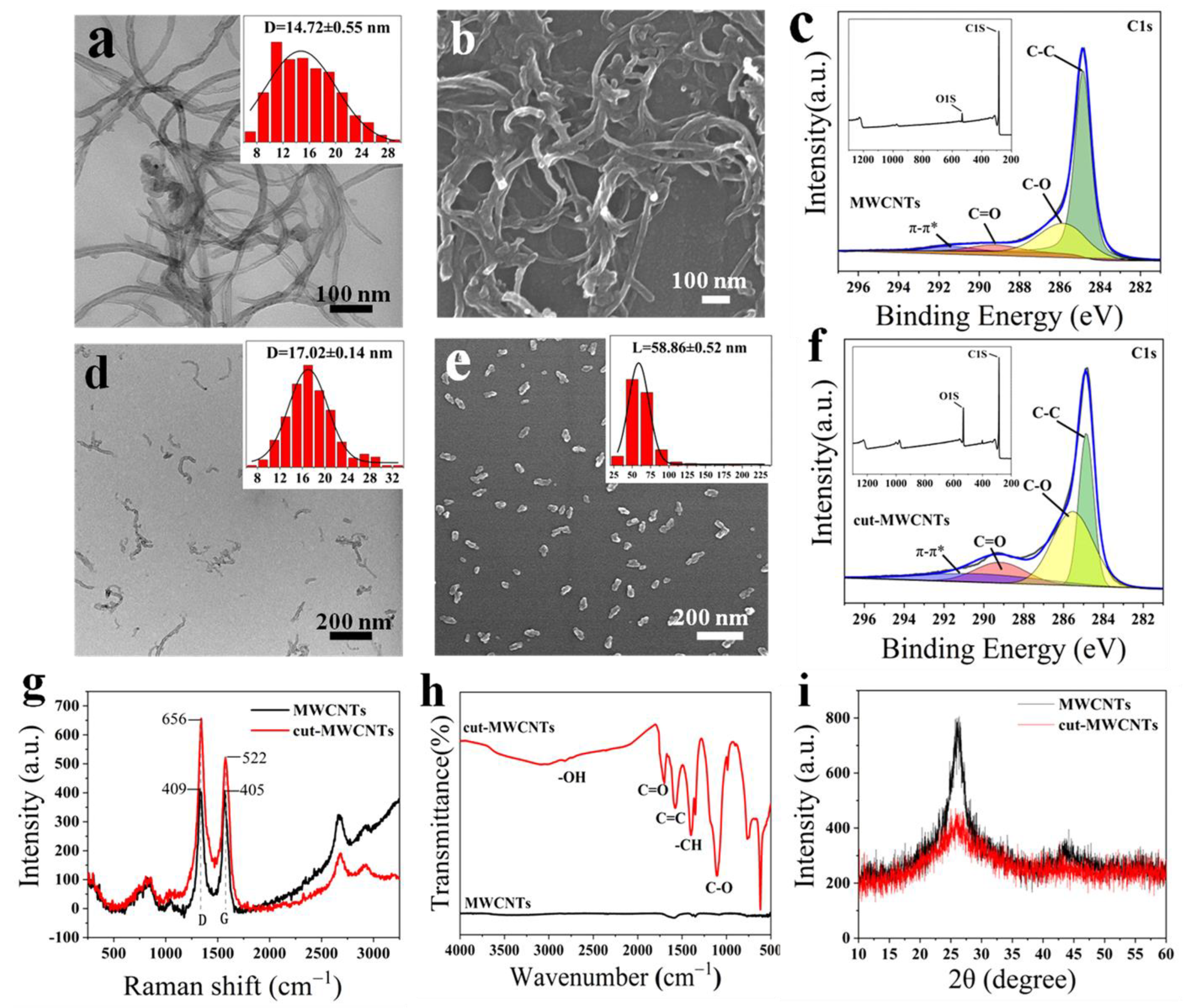
3.1. Characterizations of Cut-MWCNTs

MWCNTs often contain high-density pentagonal and heptagonal defects on the sidewalls of the nanotubes [28]. During the mixed-acid oxidation process, these positions will be preferentially destroyed. Figure 2a,b show the TEM and FESEM images of MWCNTs, respectively. It can be seen that the length of MWCNTs is so long that the tubes are entangled with each other, and the average diameter of the MWCNTs is calculated to be 14.72 ± 0.55 nm (counted number: 500). Figure 2d,e show the TEM and FESEM images of cut-MWCNTs, respectively. It can be seen that the length of cut-MWCNTs becomes shorter, and the dispersibility becomes better. Due to the uneven distribution of defects on the surface of carbon nanotubes, the length distribution of cut-MWCNTs is uneven, the average length of cut-MWCNTs is 58.86 ± 0.52 nm (counted number: 500), and the average diameter is 17.02 ± 0.14 nm (counted number: 500). This is because, during the oxidation process, the walls of the carbon nanotubes are destroyed. By comparison, it can be concluded that the ratio of the length to the diameter of cut-MWCNTs is significantly smaller than that of MWCNTs.
The Raman spectra provide molecular vibration and rotation information. Through the analysis of the position and intensity of the characteristic peaks in the spectrum of MWCNTs and cut-MWCNTs, changes in the composition and structure can be discerned. Figure 2g shows the Raman spectra of MWCNTs and cut-MWCNTs. The spectra of MWCNTs and cut-MWCNTs contain D and G peaks. The D peak at 1345 cm−1 is related to the structural defects of MWCNTs, carbon nanoparticles adsorbed on the tube wall, amorphous carbon, and other factors, which are generally considered to be caused by the defects of MWCNTs. The G peak at 1592 cm−1 is due to the sp2 hybridization of carbon atoms. The ratio of the D peak to the G peak, R, is used to characterize the structure of carbon nanotubes. The R value of MWCNTs is 1.01, and the cut-MWCNTs have an increased R of 1.26, indicating that part of the ordered graphene structure was destroyed by the acid treatment used for cutting [29].
Mixed-acid treatment will introduce acidic groups to the surface of the carbon nanotubes [30]. Cut-MWCNTs were analyzed by infrared spectroscopy, and the types of functional groups were determined according to the positions of absorption peaks. Figure 2h shows the infrared spectra of MWCNTs and cut-MWCNTs. Compared with MWCNTs, cut-MWCNTs have a wide peak at 3500–2000 cm−1, which is caused by the stretching vibration of -OH, meaning that acid treatment can introduce -OH to the surface of cut-MWCNTs. The peak at 1707 cm−1 is associated with the C=O stretching of carboxylic acids. The absorption peak near 1580 cm−1 corresponds to the stretching vibration of the C=C bond, which is inherent in the structure of carbon nanotubes. The peaks at 1404 cm−1 and 1100 cm−1 are obviously enhanced, corresponding to the in-plane bending vibration of -CH and the stretching vibration of C-O, respectively. These absorption peaks indicate that there are a large number of oxygen-containing functional groups on the surface of cut-MWCNTs, which increase the negative surface charge and enhance the electrostatic repulsion between cut-MWCNTs. The strong electrostatic repulsion makes the dispersion of carbon nanotubes in solution more uniform and prevents aggregation. This is consistent with the TEM and FESEM results and is conducive to the deposition of cut-MWCNTs on the surface of TiO2-NTs by electrophoresis.
The XRD patterns reflect the crystalline structural features of MWCNTs and cut-MWCNTs, which were tested under the same conditions. As shown in Figure 2i, the peak at 26.1° is the diffraction peak of the graphitic layer structure (002), from which the crystalline structural changes in carbon nanotubes before and after cutting can be seen. The peak of pristine MWCNTs is sharper and stronger. However, the peak of cut-MWCNTs at 26.1° is broader and much lower, and the intensity drops significantly, indicating that the initial graphitic structure of MWCNTs is oxidized and has more amorphous features. A large number of oxygen-containing functional groups change the atomic arrangement of MWCNTs.
The surface properties of MWCNTs and cut-MWCNTs were studied by N2 adsorption analysis. As can be seen from the nitrogen (N2) adsorption–desorption isotherm in Figure S2a, the samples have obvious lag loops at relative pressures between 0.7 and 1.0, indicating the existence of mesopores. The carbon nanotubes show an increase in the surface area from 105 m2/g to 155 m2/g due to oxidative cutting. The increase in the specific surface area can be attributed to the combined effect of the unbundling of MWCNTs and the opening of end caps, leading to a higher uptake of nitrogen at a relative pressure of 0.7 to 1.0 in the cut-MWCNTs due to the increase in mesopores [31], while the length of cut-MWCNTs is shorter and can achieve better contact with TiO2-NTs. In addition, the slight N2 uptake at low pressures suggests the co-existence of micropores. The NL-DFT pore size distribution further verifies the pore structure, showing that the main pores are centered in a wide range of 1–10 nm (Figure S2b). It is interesting to find that there is a new fraction of pores at 3.4 nm for cut-MWCNTs, suggesting that pickling is beneficial to the formation of mesopores.
To further study the chemical bonding of MWCNTs in the oxidized state, we carried out XPS characterization of the MWCNTs and cut-MWCNTs. The spectra of C1s before and after oxidation (Figure 2c,f) can be divided into four peaks. The peak areas corresponding to C-O and C=O increased significantly after oxidation. Table 1 lists the elemental composition of MWCNTs and cut-MWCNTs, also showing a significant increase in the oxygen atom percentage after oxidation. MWCNTs can be regarded as coiled multilayer graphene. Mixed-acid oxidation consumes π-conjugated groups and introduces oxygen-containing functional groups between graphite layers [32], which is consistent with the FT-IR results. In addition, the contents of N and S are also increased slightly, but the remaining N and S functional groups have no mobility after the strong and repeated washing process, so they have no influence on the device efficiency.

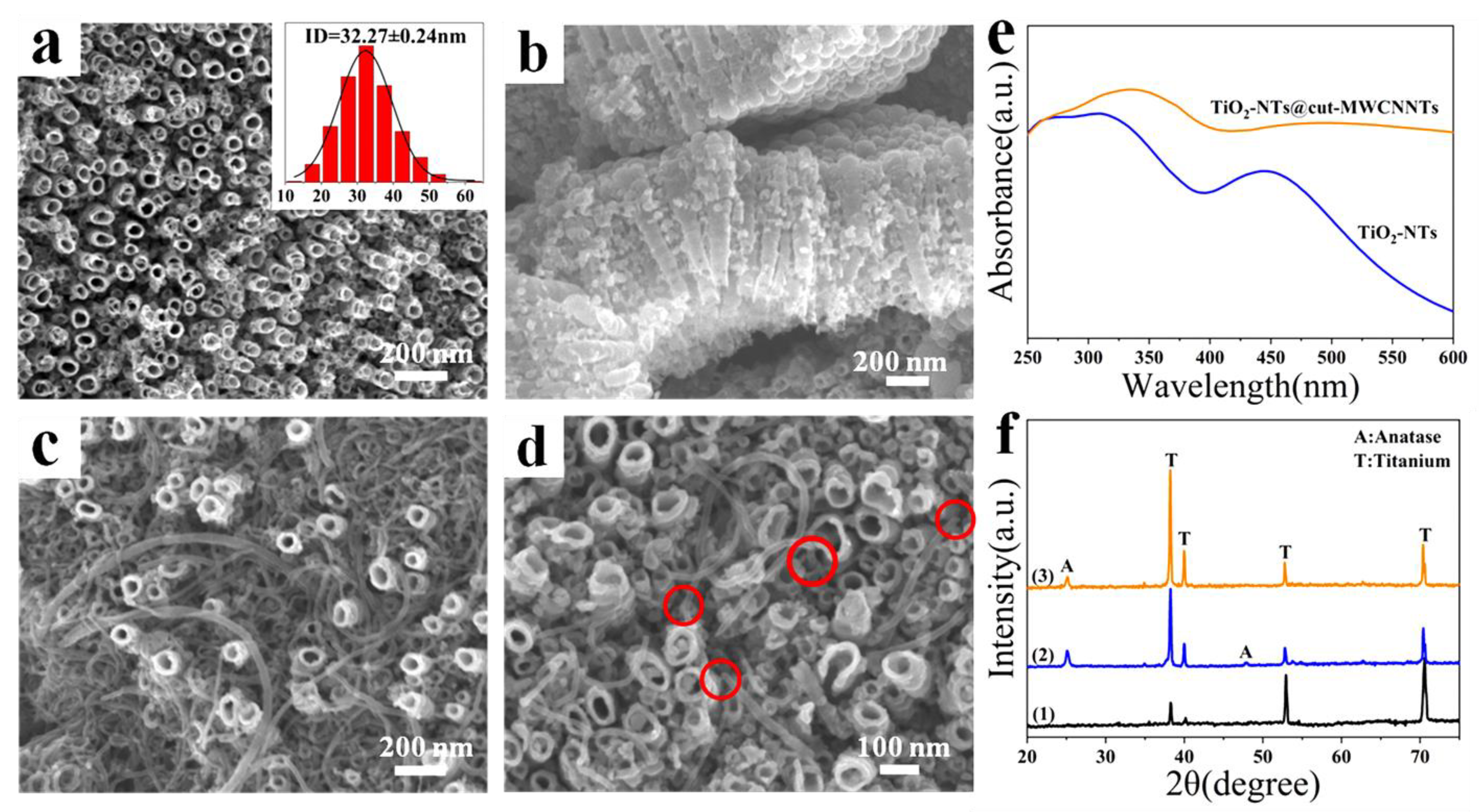
3.2. Characterizations of TiO2-NTs@cut-MWCNT Heterostructure

Figure 3a,b show SEM images of pure TiO2-NTs. The pure TiO2-NTs indicate a clear tubular structure. The average inner diameter is 32.27 ± 0.24 nm, and the tube lengths are about 600~700 nm. Figure 3c,d are SEM images of TiO2-NTs@cut-MWCNTs, in which the deposited cut-MWCNTs can be found in the pores and gaps among the TiO2-NTs, as marked in Figure 3d (Figure S3 is a cross-sectional SEM image of the TiO2-NTs@cut-MWCNT heterostructure).
To demonstrate the effect of cut-MWCNTs on the light absorption properties of TiO2-NTs, Figure 3e shows the UV-vis absorption spectra of TiO2-NTs and TiO2-NTs@cut-MWCNTs. Compared with TiO2-NTs, the light absorption of the TiO2-NTs@cut-MWCNT heterostructure significantly increased, and at the same time, its absorption edge was red-shifted from 310 nm to 336 nm, indicating that due to the recombination of cut-MWCNTs, the energy band of TiO2-NTs is narrower and is more readily excited by visible light.
XRD was employed to characterize the crystalline phase of the TiO2-NTs@cut-MWCNT heterostructure, as shown in Figure 3f. Before the annealing of TiO2-NTs, all peaks were attributed to the Ti substrate. After annealing, peaks appeared at 25.1° and 48°, corresponding to the (101) and (200) crystal planes of the anatase phase of TiO2, indicating that annealing changed the crystal form of TiO2 from the amorphous phase to the anatase phase. Anatase TiO2 is a relatively stable structure with high band-gap energy. There are more defects and vacancies in the lattice, resulting in more oxygen vacancies to capture electrons, so it has high activity. In the XRD patterns of the TiO2-NTs@cut-MWCNT heterostructure, the (101) plane (2θ = 25.1°) of the anatase phase can be seen. However, there are almost no diffraction peaks to be found for cut-MWCNTs. This is because the cut-MWCNTs have a broad and weak diffraction peak at 2θ = 26.1°, as shown in Figure 2i, indicating very weak crystalline characteristics. Thus, in the TiO2-NTs@cut-MWCNTs, the lower content of cut-MWCNTs results in a signal that is too weak to detect.

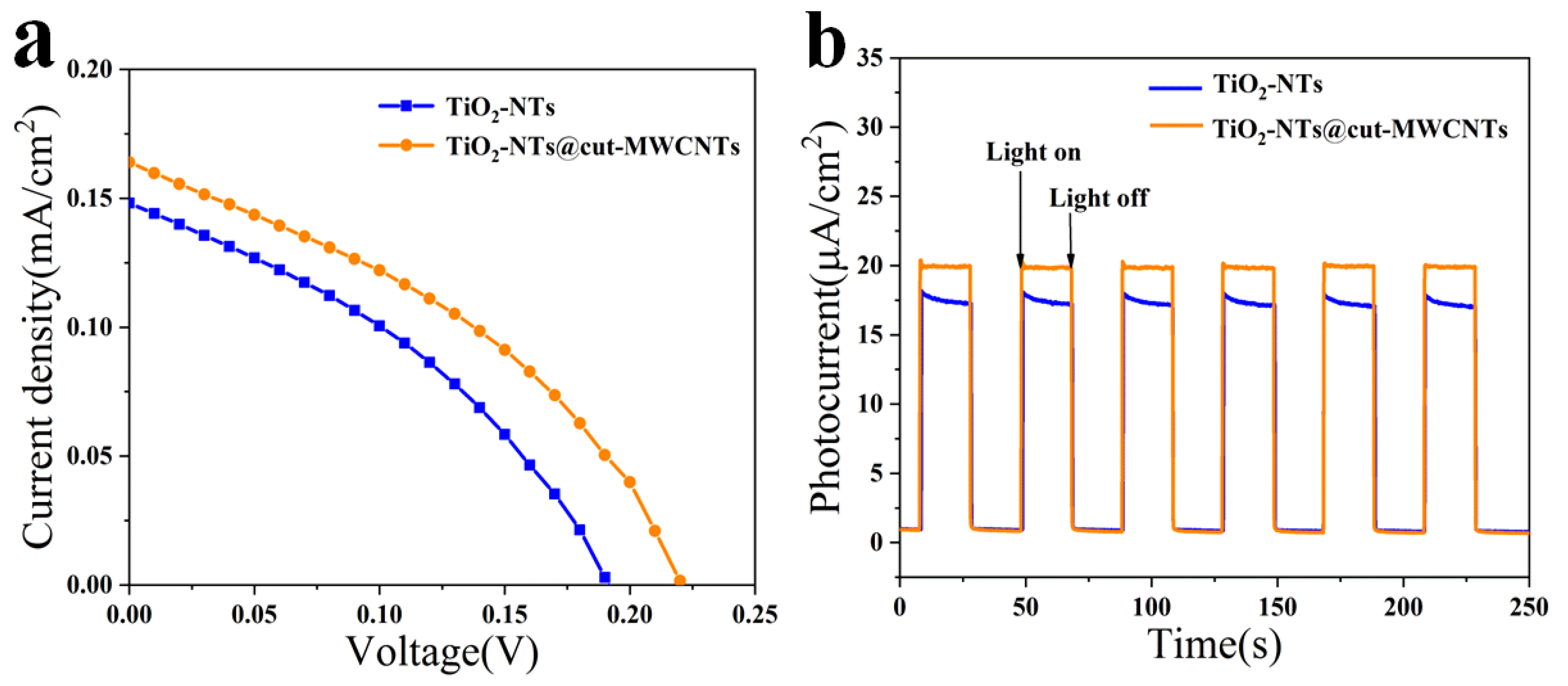
3.3. Characterizations of All-Titanium–Carbon Photovoltaic Device

The TiO2-NT and TiO2-NTs@cut-MWCNT heterostructures were each assembled into photovoltaic devices, and the current-density–voltage (J-V) characteristics were recorded using a solar simulator under AM 1.5 G solar illumination; the active area of the device was 0.25 cm2. We determined the efficiency of five devices and averaged the data. The results are shown in Figure 4a, and the device parameters are listed in Table 2. Compared with the devices based on pure TiO2-NTs, the device efficiency based on TiO2-NTs@cut-MWCNTs improved to 0.0138%. This is because the cut-MWCNTs have better light absorption properties and promote the efficient separation of photogenerated charges.
In order to evaluate the charge transfer of the as-synthesized TiO2-NTs@cut-MWCNT heterostructures, the transient photocurrent response of TiO2-NT and TiO2-NTs@cut-MWCNT heterostructures was studied by using a CEL-S500/350 xenon lamp, a CHI-660E workstation, and a control system to build a simulated sunlight test device. A standard three-electrode system was used, with a Pt sheet as the counter electrode, AgCl as the reference electrode, TiO2-NTs or TiO2-NTs@cut-MWCNTs as the working electrode, and a 0.1 M Na2S aqueous solution as the electrolyte, under AM 1.5 G light intensity. The transient photogenerated current density test time was 400 s, and the interval between turning the light source on and off was 20 s. In Figure 4b, it can be seen that the photocurrent density of TiO2-NTs is 17.48 μA/cm2, and the photocurrent density of the TiO2-NTs@cut-MWCNT heterostructure is 19.94 μA/cm2, exhibiting a significantly enhanced transient photocurrent. The density response is due to: (i) the enhanced absorption of visible light by the TiO2-NTs@cut-MWCNT heterostructure generating a greater number of carriers under illumination and (ii) the enhanced separation of photogenerated carriers prolonging the electron lifetime.
This work represents the first attempt at the construction of all-titanium–carbon photovoltaic devices. There are many factors that affect the photovoltaic performance. For example, we can achieve better charge transmission by improving the contact density of cut-MWCNTs and TiO2-NTs so as to improve the efficiency of photovoltaic devices.

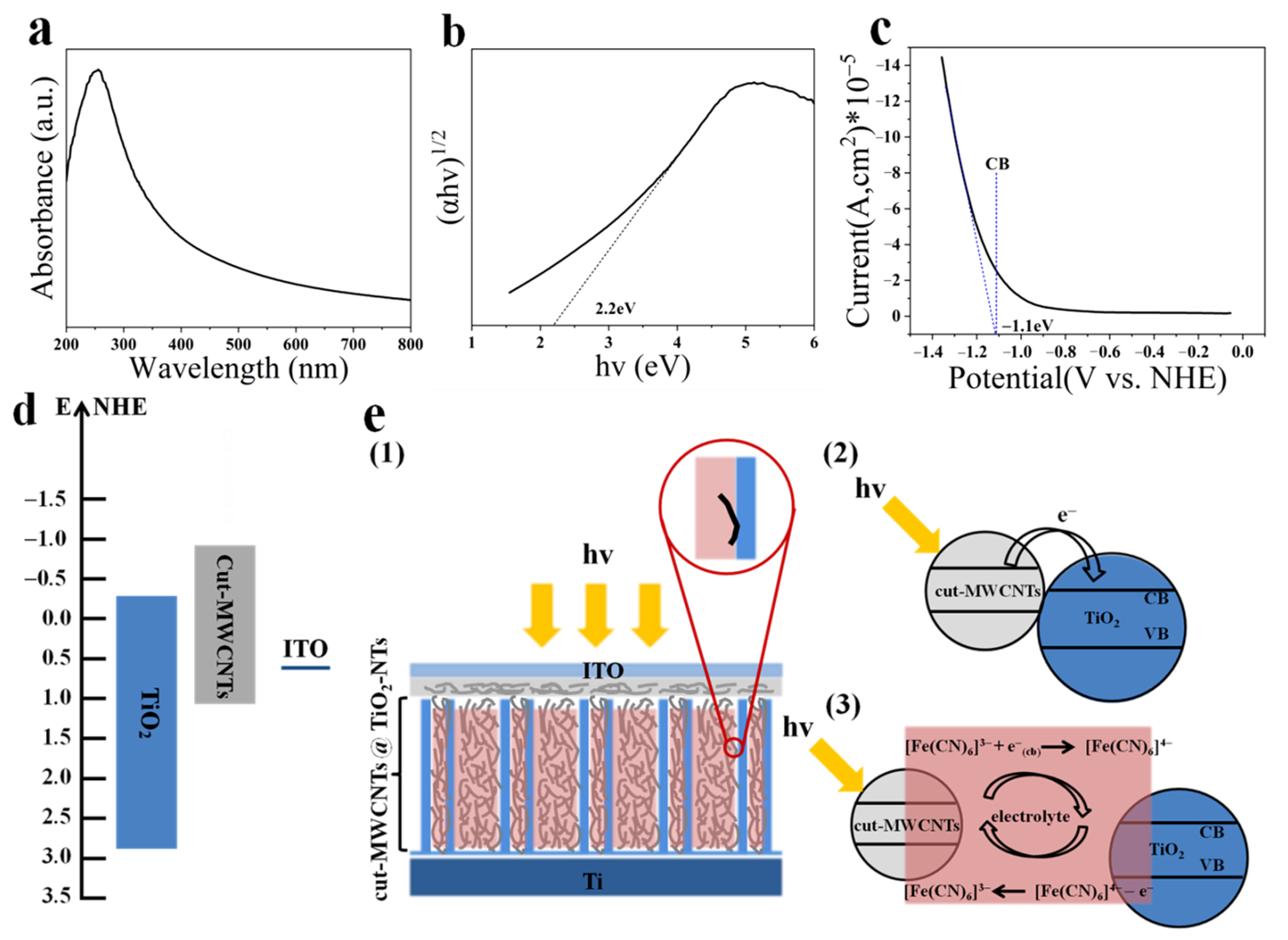
3.4. Mechanism of Photocurrent Generation

We calculated the band gap by the Kubelka–Munk function. Figure S4 shows the band gap of TiO2-NTs. The (αhν)1/2 of hν in the vicinity of the absorption edge is plotted for TiO2-NTs in Figure 3e, where hν is the photo energy, and the reflectance is converted to an equivalent absorption coefficient by α = (1 − R)2/2R [33]. Figure 3e shows that the light absorption range of TiO2-NTs is mostly in the ultraviolet region, which means that higher energy absorption is required for electronic transitions to occur; by extrapolating the linear part of the curve to the intersection with the x-axis, its band gap is estimated to be 3.18 eV, which is in line with the band-gap width of anatase TiO2 [34]. Generally, the oxidation of graphene will open the electron energy gap, and an increased degree of oxidation results in a larger band gap [35,36]. In addition, graphene oxide has been found to be a p-type or n-type semiconductor [37,38]. Therefore, the band gap of carbon nanotubes can be tuned by different degrees of oxidation to meet specific photovoltaic applications.
Through the optical absorption spectrum and the linear potential scan, the energy-level position of the cut-MWCNTs can be obtained. Figure 5a shows the UV-vis absorption spectrum of cut-MWCNTs. According to the Kubelka–Munk function, the forbidden bandwidth is calculated to be 2.2 eV [39], as shown in Figure 5b. Figure 5c shows that the conduction band position of cut-MWCNTs is calculated to be −1.1 eV (vs. NHE) by linear potential scanning [39]. Figure 5d shows the energy-level schematic diagram of TiO2 and cut-MWCNTs.
The electron transport mechanism in photovoltaic devices is shown in Figure 5e. Figure 5e (1) is a cross-sectional view of the photovoltaic device. TiO2 and carbon nanotubes are connected by direct contact and electrolyte contact, so we conclude that the photocurrent is generated mainly through the following two pathways: (i) Direct-contact electron conduction, as shown in Figure 5e (2). The photoexcitation of cut-MWCNTs leads to rapid electron injection into TiO2. (ii) Indirect-contact electron conduction, as shown in Figure 5e (3). The electrolyte acts as a “bridge”, whereby cut-MWCNTs are excited by light to generate electrons, and the oxidized electrolyte [Fe(CN)6]3− accepts electrons and changes to the reduced state [Fe(CN)6]4−. TiO2 then oxidizes [Fe(CN)6]4− to [Fe(CN)6]3−. The reactions are:
(cut-MWCNTs) + hν → (cut-MWCNTs)*
(cut-MWCNTs)* → (cut-MWCNTs)+ + e(cb)
[Fe(CN)6]3− + e(cb) → [Fe(CN)6]4−
TiO2 + [Fe(CN)6]4− → (TiO2) + [Fe(CN)6]3−

4. Conclusions

In conclusion, we prepared highly ordered TiO2-NTs on a metal Ti substrate by anodic oxidation. Short cut-MWCNTs were obtained by chemical oxidation. The tests and analyses showed that the graphene structure of MWCNTs was destroyed, and a large number of negatively charged oxygen-containing functional groups were introduced to the surface. Under the action of an external electric field, cut-MWCNTs were filled into TiO2-NTs to form the TiO2-NTs@cut-MWCNT heterostructure. The test results show that the two materials effectively combined. Chemically modified MWCNTs have a band gap of 2.2 eV and have a suitable energy level matching that of TiO2. Compared with pure TiO2-NTs, the TiO2-NTs@cut-MWCNT heterostructure exhibits higher light absorption and a higher transient photocurrent density, and the fabricated photovoltaic device efficiency increases from 0.01036% to 0.01380%.
This is a new attempt to adjust the band gap of carbon nanotubes through oxidation to achieve energy level matching with TiO2 and to prepare photovoltaic devices with semiconducting carbon nanotubes as photosensitizers. We hope this study provides a reference for the application of carbon nanotubes in photovoltaic devices and promotes the further development for the efficient large-scale production of all-titanium–carbon photovoltaic devices.

Supplementary Materials

The following supporting information can be downloaded at: https://www.mdpi.com/article/10.3390/nano12203604/s1, Figure S1: Schematic diagram of the electrophoresis device; Figure S2: (a) N2 adsorption-desorption isotherms; (b) NL-DFT pore size distributions of MWCNTs and cut-MWCNTs; Figure S3: Cross-sectional SEM image of the TiO2-NTs@cut-MWCNTs heterostructure; Figure S4: Kubelka-Munk function for band gap estimation of TiO2-NTs.

Author Contributions

S.N.: data curation, formal analysis, writing—original draft preparation, and writing—review and editing. W.Y.: supervision. H.W.: supervision. M.D.: supervision. I.R.: supervision. K.C.P.: conceptualization and writing—review and editing. Y.W.: supervision. M.J.K.: writing—review and editing. L.A.B.: supervision. J.T.: methodology, conceptualization, writing—review and editing, and funding acquisition. All authors have read and agreed to the published version of the manuscript.

Funding

This work was supported by (1) the National Natural Science Foundation of China (51473082 and 51878361); (2) the State Key Project of International Cooperation Research (2016YFE0110800 and 2017YFE0108300); (3) the National Program for Introducing Talents of Discipline to Universities (“111” plan); (4) 1st Class Discipline Program of Materials Science of Shandong Province; and (5) The Double-Hundred Foreign Expert Program of Shandong Province.

Data Availability Statement

All data, models, and code generated or used during the study appear in the submitted article.

Conflicts of Interest

The authors declare no conflict of interest.

References

  1. Lewis, N.S. Toward cost-effective solar energy use. Science 2007, 315, 798–801. [Google Scholar] [CrossRef] [Green Version]
  2. Tang, C.W. 2-Layer Organic Photovoltaic Cell. Appl. Phys. Lett. 1986, 48, 183–185. [Google Scholar] [CrossRef]
  3. Oregan, B.; Gratzel, M. A Low-Cost, High-Efficiency Solar-Cell Based on Dye-Sensitized Colloidal TiO2 Films. Nature 1991, 353, 737–740. [Google Scholar] [CrossRef]
  4. Mariotti, N.; Bonomo, M.; Fagiolari, L.; Barbero, N.; Gerbaldi, C.; Bella, F.; Barolo, C. Recent advances in eco-friendly and cost-effective materials towards sustainable dye-sensitized solar cells. Green Chem. 2020, 22, 7168–7218. [Google Scholar] [CrossRef]
  5. Gong, D.; Grimes, C.A.; Varghese, O.K.; Hu, W.C.; Singh, R.S.; Chen, Z.; Dickey, E.C. Titanium oxide nanotube arrays prepared by anodic oxidation. J. Mater. Res. 2001, 16, 3331–3334. [Google Scholar] [CrossRef] [Green Version]
  6. Paulose, M.; Shankar, K.; Varghese, O.K.; Mor, G.K.; Hardin, B.; Grimes, C.A. Backside illuminated dye-sensitized solar cells based on titania nanotube array electrodes. Nanotechnology 2006, 17, 1446–1448. [Google Scholar] [CrossRef]
  7. Ito, S.; Ha, N.L.C.; Rothenberger, G.; Liska, P.; Comte, P.; Zakeeruddin, S.M.; Pechy, P.; Nazeeruddin, M.K.; Gratzel, M. High-efficiency (7.2%) flexible dye-sensitized solar cells with Ti-metal substrate for nanocrystalline-TiO2 photoanode. Chem. Commun. 2006, 4004–4006. [Google Scholar] [CrossRef]
  8. Wu, J.H.; Xiao, Y.M.; Tang, Q.W.; Yue, G.T.; Lin, J.M.; Huang, M.L.; Huang, Y.F.; Fan, L.Q.; Lan, Z.; Yin, S.; et al. A Large-Area Light-Weight Dye-Sensitized Solar Cell based on All Titanium Substrates with an Efficiency of 6.69% Outdoors. Adv. Mater. 2012, 24, 1884–1888. [Google Scholar] [CrossRef]
  9. Nyein, N.; Tan, W.K.; Kawamura, G.; Matsuda, A.; Lockman, Z. TiO2 nanotube arrays formation in fluoride/ethylene glycol electrolyte containing LiOH or KOH as photoanode for dye-sensitized solar cell. J. Photochem. Photobiol. A-Chem. 2017, 343, 33–39. [Google Scholar] [CrossRef]
  10. He, W.; Qiu, J.J.; Zhuge, F.W.; Li, X.M.; Lee, J.H.; Kim, Y.D.; Kim, H.K.; Hwang, Y.H. Advantages of using Ti-mesh type electrodes for flexible dye-sensitized solar cells. Nanotechnology 2012, 23, 6. [Google Scholar] [CrossRef]
  11. Zha, C.Y.; Shen, L.M.; Zhang, X.Y.; Wang, Y.F.; Korgel, B.A.; Gupta, A.; Bao, N.Z. Double-Sided Brush-Shaped TiO2 Nanostructure Assemblies with Highly Ordered Nanowires for Dye-Sensitized Solar Cells. Acs Appl. Mater. Interfaces 2014, 6, 122–129. [Google Scholar] [CrossRef]
  12. Castrucci, P.; Scilletta, C.; Del Gobbo, S.; Scarselli, M.; Camilli, L.; Simeoni, M.; Delley, B.; Continenza, A.; De Crescenzi, M. Light harvesting with multiwall carbon nanotube/silicon heterojunctions. Nanotechnology 2011, 22, 8. [Google Scholar] [CrossRef]
  13. Castrucci, P.; Tombolini, F.; Scarselli, M.; Speiser, E.; Del Gobbo, S.; Richter, W.; De Crescenzi, M.; Diociaiuti, M.; Gatto, E.; Venanzi, M. Large photocurrent generation in multiwall carbon nanotubes. Appl. Phys. Lett. 2006, 89, 3. [Google Scholar] [CrossRef]
  14. El Khakani, M.A.; Le Borgne, V.; Aissa, B.; Rosei, F.; Scilletta, C.; Speiser, E.; Scarselli, M.; Castrucci, P.; De Crescenzi, M. Photocurrent generation in random networks of multiwall-carbon-nanotubes grown by an “all-laser” process. Appl. Phys. Lett. 2009, 95, 3. [Google Scholar] [CrossRef]
  15. Scarselli, M.; Scilletta, C.; Tombolini, F.; Castrucci, P.; De Crescenzi, M.; Diociaiuti, M.; Casciardi, S.; Gatto, E.; Venanzi, M. Photon harvesting with multi wall carbon nanotubes. Superlattices Microstruct. 2009, 46, 340–346. [Google Scholar] [CrossRef] [Green Version]
  16. Scarselli, M.; Scilletta, C.; Tombolini, F.; Castrucci, P.; Diociaiuti, M.; Casciardi, S.; Gatto, E.; Venanzi, M.; De Crescenzi, M. Multiwall Carbon Nanotubes Decorated with Copper Nanoparticles: Effect on the Photocurrent Response. J. Phys. Chem. C 2009, 113, 5860–5864. [Google Scholar] [CrossRef]
  17. Sarker, B.K.; Arif, M.; Stokes, P.; Khondaker, S.I. Diffusion mediated photoconduction in multiwalled carbon nanotube films. J. Appl. Phys. 2009, 106, 4. [Google Scholar] [CrossRef] [Green Version]
  18. Ou, Y.; Lin, J.D.; Fang, S.M.; Liao, D.W. MWNT-TiO2: Ni composite catalyst: A new class of catalyst for photocatalytic H-2 evolution from water under visible light illumination. Chem. Phys. Lett. 2006, 429, 199–203. [Google Scholar] [CrossRef]
  19. Kierkowicz, M.; Pach, E.; Santidrian, A.; Sandoval, S.; Goncalves, G.; Tobias-Rossell, E.; Kalbac, M.; Ballesteros, B.; Tobias, G. Comparative study of shortening and cutting strategies of single-walled and multi-walled carbon nanotubes assessed by scanning electron microscopy. Carbon 2018, 139, 922–932. [Google Scholar] [CrossRef]
  20. Kumar, S.S.; Vairam, S.; Neelakandeswari, N.; Aruna, S. Effect of metal oxide charge transfer layers on the photovoltaic performance of carbon nanotube heterojunction solar cells. Mater. Lett. 2018, 220, 249–252. [Google Scholar] [CrossRef]
  21. Kalita, G.; Adhikari, S.; Aryal, H.R.; Umeno, M.; Afre, R.; Soga, T.; Sharon, M. Cutting carbon nanotubes for solar cell application. Appl. Phys. Lett. 2008, 92, 3. [Google Scholar] [CrossRef]
  22. Baker, B.A.; Zhang, H.; Cha, T.G.; Choi, J.H. 9—Carbon nanotube solar cells. In Carbon Nanotubes and Graphene for Photonic Applications; Yamashita, S., Saito, Y., Choi, J.H., Eds.; Woodhead Publishing: Sawston, UK, 2013; pp. 241–269. [Google Scholar] [CrossRef]
  23. Macak, J.M.; Gong, B.G.; Hueppe, M.; Schmuki, P. Filling of TiO2 Nanotubes by Self-Doping and Electrodeposition. Adv. Mater. 2007, 19, 3027–3031. [Google Scholar] [CrossRef]
  24. Hoffmann, M.R.; Martin, S.T.; Choi, W.; Bahnemann, D.W. Environmental Applications of Semiconductor Photocatalysis. Chem. Rev. 1995, 95, 69–96. [Google Scholar] [CrossRef]
  25. Wang, W.; Serp, P.; Kalck, P.; Faria, J. Visible Light Photodegradation of Phenol on MWNT-TiO2 Composite Catalysts Prepared by a Modified Sol–Gel Method. J. Mol. Catal. A Chem. 2005, 235, 194–199. [Google Scholar] [CrossRef]
  26. Banerjee, S.; Wong, S. Synthesis and Characterization of Carbon Nanotube−Nanocrystal Heterostructures. Nano Lett.-NANO LETT 2002, 2, 195. [Google Scholar] [CrossRef]
  27. Su, B.Z.; Wang, S.C.; Yang, W.B.; Wang, Y.; Huang, L.J.; Popat, K.C.; Kipper, M.J.; Belfiore, L.A.; Tang, J.G. Synthesis of Eu-modified luminescent Titania nanotube arrays and effect of voltage on morphological, structural and spectroscopic properties. Mater. Sci. Semicond. Process. 2020, 113, 9. [Google Scholar] [CrossRef]
  28. Dai, H.J. Carbon nanotubes: Opportunities and challenges. Surf. Sci. 2002, 500, 218–241. [Google Scholar] [CrossRef]
  29. Song, Y.P.; Feng, M.; Zhan, H.B. Electrochemistry of partially unzipped carbon nanotubes. Electrochem. Commun. 2014, 45, 95–98. [Google Scholar] [CrossRef]
  30. Saito, T.; Matsushige, K.; Tanaka, K. Chemical treatment and modification of multi-walled carbon nanotubes. Phys. B 2002, 323, 280–283. [Google Scholar] [CrossRef]
  31. Li, F.; Wang, Y.; Wang, D.; Wei, F. Characterization of single-wall carbon nanotubes by N2 adsorption. Carbon 2004, 42, 2375–2383. [Google Scholar] [CrossRef]
  32. Iijima, S. Helical Microtubules of Graphitic Carbon. Nature 1991, 354, 56–58. [Google Scholar] [CrossRef]
  33. Reyes-Coronado, D.; Rodríguez-Gattorno, G.; Espinosa-Pesqueira, M.E.; Cab, C.; de Coss, R.; Oskam, G. Phase-pure TiO2nanoparticles: Anatase, brookite and rutile. Nanotechnology 2008, 19, 145605. [Google Scholar] [CrossRef]
  34. Gong, J.W.; Liang, J.; Sumathy, K. Review on dye-sensitized solar cells (DSSCs): Fundamental concepts and novel materials. Renew. Sust. Energ. Rev. 2012, 16, 5848–5860. [Google Scholar] [CrossRef]
  35. Boukhvalov, D.W.; Katsnelson, M.I. Modeling of graphite oxide. J. Am. Chem. Soc. 2008, 130, 10697–10701. [Google Scholar] [CrossRef] [PubMed] [Green Version]
  36. Wang, D.H.; Choi, D.W.; Li, J.; Yang, Z.G.; Nie, Z.M.; Kou, R.; Hu, D.H.; Wang, C.M.; Saraf, L.V.; Zhang, J.G.; et al. Self-Assembled TiO2-Graphene Hybrid Nanostructures for Enhanced Li-Ion Insertion. ACS Nano 2009, 3, 907–914. [Google Scholar] [CrossRef] [Green Version]
  37. Wu, X.S.; Sprinkle, M.; Li, X.B.; Ming, F.; Berger, C.; de Heer, W.A. Epitaxial-graphene/graphene-oxide junction: An essential step towards epitaxial graphene electronics. Phys. Rev. Lett. 2008, 101, 4. [Google Scholar] [CrossRef] [Green Version]
  38. Gilje, S.; Han, S.; Wang, M.; Wang, K.L.; Kaner, R.B. A chemical route to graphene for device applications. Nano Lett. 2007, 7, 3394–3398. [Google Scholar] [CrossRef]
  39. Yeh, T.F.; Chan, F.F.; Hsieh, C.T.; Teng, H.S. Graphite Oxide with Different Oxygenated Levels for Hydrogen and Oxygen Production from Water under Illumination: The Band Positions of Graphite Oxide. J. Phys. Chem. C 2011, 115, 22587–22597. [Google Scholar] [CrossRef]
Figure 1. Schematic diagram of experimental process and device structure.
Nanomaterials 12 03604 g001
Figure 2. Pristine MWCNT morphology observed by (a) TEM and (b) FESEM; (c) XPS C1s spectrum of MWCNTs, with the survey scan shown in the inset; cut-MWCNT morphology observed by (d) TEM and (e) FESEM; (f) XPS C1s spectrum of cut-MWCNTs, with the survey scan shown in the inset; (g) Raman spectra of MWCNTs and cut-MWCNTs; (h) FT-IR spectra of MWCNTs and cut-MWCNTs; (i) XRD patterns of MWCNTs and cut-MWCNTs.
Nanomaterials 12 03604 g002
Figure 3. SEM images of TiO2-NTs (a,b) and TiO2-NTs@cut-MWCNTs (c,d); (e) UV-vis absorbance spectra of TiO2-NTs and TiO2-NTs@cut-MWCNTs; (f) XRD patterns of TiO2-NTs before (1) and after annealing (2) and the TiO2-NTs@cut-MWCNTs (3).
Nanomaterials 12 03604 g003
Figure 4. (a) J-V curves of devices based on TiO2-NTs and TiO2-NTs@cut-MWCNTs; (b) the transient photocurrent density under visible light and dark conditions for TiO2-NTs and TiO2-NTs@cut-MWCNTs.
Nanomaterials 12 03604 g004
Figure 5. (a) Optical absorption spectra of cut-MWCNTs; (b) plots of (αhν)1/2 against the photon energy (hν) for cut-MWCNTs; (c) cathodic linear potential scan for determining the conduction band (CB) edge of the cut-MWCNTs; (d) schematic diagram of device energy level; (e) electron transport mechanisms in photovoltaic devices.
Nanomaterials 12 03604 g005
Table 1. Elemental composition of MWCNTs and cut-MWCNTs.
SampleC [%]O [%]N [%]S [%]
MWCNTs95.74.3----
cut-MWCNTs82.5515.461.570.42
Table 2. Photovoltaic device parameters based on TiO2-NTs and TiO2-NTs@cut-MWCNTs.
SampleVoc (V)Jsc (mA/cm2)FF [%]PCE [%]
TiO2-NTs0.190.1480.3650.01036
TiO2-NTs@cut-MWCNTs0.220.1640.3810.01380
Publisher’s Note: MDPI stays neutral with regard to jurisdictional claims in published maps and institutional affiliations.

